Note: Descriptions are shown in the official language in which they were submitted.
~2~ 3
The present invention relates to a Galois field arithmetic
logic unit of a code error check and correct apparatus
employed for recording and reproducing data on an optical
disk.
: 5 The present invention will be illustrated by way of the
accompanying drawings in which:
FIGs. lA and lB are flowcharts illustrating a first
embodiment according to the present invention;
FIG. lC is a schematic block diagram showing a configuration
of a Galois field arithmetic logic unit to which the first
embodiment of the present invention is applied;
FIGs. 2A and 2B are flowcharts illustrating a second
embodiment according to the present invention;
. ~
FIG. 2C is a schematic block diagram showing a configuration
of a Galois field arithmetic logic unit to which the second
embodiment of the present invention is applied;
FIG. 3 is a schematic block diagram showing a configuration
of a Galois field arithmetic logic unit to which a third
embodiment of the present invention is applied;
FIG. 4 is a schematic block diagram showing a configuration
of a Galois field arithmetic logic unit of a prior art
example; and
FIG. 5 is a schematic block diagram showing a configuration
of a Galois f.ield multiplier circuit of a prior art example.
Recently, there has been achieved an intensive developmen-t of
: data record/reproduce apparatuses using an optical disk.
~7661 ~3
Although the optical disk memory generally enables to record
therein a greater amount of data as compared with a magnetic
~ disk, the rscording medium of the optical disk memory has a
! disadvantage that a higher raw error rate results.
To overcome this difficulty, there has been commonly employed
a method in which error correcting codes are added to data
when recording the data so as to record both the data and the
error correcting codes on an optical disk and then a data
error is detected and is corrected by use of the error
correcting codes when reproducing the recorded data. As such
an error correcting code, the Reed-Solomon code with a
Hamming distance d = about 17 has attracted attention these
days.
For decoding of the Reed-Solomon code,
- la -
~27~ L3
l syndromes are first calculated from a received word
and then an error location polynomial ~ (x) and an error
value polynomial ~ (x) are attained from the syndrome.
Finally, an error location and an error value are
estimated from these polynomials so as to effect a
correction; however, due to the great hamming distance,
the decoding process becomes to be complicated and
hence takes a long period of time; furthermore, a
large-sized circuit is necessary to implement the
decoding process by means of a hardware system.
Since the calculation of the syndrome greatly
influences the decode speed, a parallel operation
hardware is employed in many cases. In a case where
particularly a high-speed operation is required, also
the other processing is effected, not by such a pure
hardware system, but b~ means of a micro-programming
scheme.
In this case, there have been used algorithms
such as the method of Barlekamp ~assey or the Euclidean
algorithm (of the mutual division) for the computations
of the error location polynomial and the error value
polinomial. In order to attain error locations from
the error location polynomial, the Chien's algorithm
is employed in which all the possible error locations
are assigned to the error location polynomial. The
error value is obtained by effecting a differential
calculation of the error location polynomial and a
calculation and a division of the error value polynomial.
~ z7~ 3
1 The Chien's algorithm, the calculation of
the differentiation of the error location polynomial,
and the calculation of the error value polynomial each
are associated with values of polynomials. Heretofore,
as a method to effect a calculation of values of a
polynomial, there has been utilized a method called
the Horner's method in which the computation is reduced
to a repetitious computation of sum of products. (Refer
to, for example, "E~igh Speed Decoding of Reed-Solomon
Codes" described in the U.S.P. 4,142,174 2/1979.)
Referring now to the accompanying drawings,
; a conventional Galois field arithmetic logic unit will be
described. FIGs. 4 and S show portions of a Galois field
arithmetic logic unit employed in a conventional code
correction processing. In FIG. 4, the configuration
incudes a 0 element decision circuit 11, input pipe-
line registers 12, 13, 34, a memory 28, a Galois field
multiplyer unit 29, a Galois field add circuit (exclusive
OR logic circuit~ 30, switch logic gate circuits 31,
32, and a power generate circuit generating a power of
a primitive element ~ cation generate circuit) 33.
The arithmetic operation is effected in GF (2r).
A received word is first deinterleaved and
the resultant word is in~utted to a code error detect
circuit, namely, a syndrome calculate circuit. If all
syndromes thus attained is other than 0, an occurrence
of an error is assumed and the syndromes are delivered
to the Galois arithmetic logic unit effecting an
1 estimation of the number of errors and computations
for coefficients of the error location polynomial,
thereby computing the error locations based on the
results.
The memory 28 is supplied with syndromes of
which the number is represented by (Hamming distance - 1)
from the syndrome calculate circuit, and then the number
t of errors and the t + 1 coefficients of the respective
degrees of the error location polynomial are computed
and are then stored by means of the multiplier 29, the
adder 30, control logic circuit using a microprogram
~not shown), an inversion memory, and the like. There-
after, also using the same Galois arithmetic logic unit,
the root of the error location polynomial is computed
according to the Chien's method.
Assuming for simplification that there exist
t~Jo errors, in order to attain the root of the error
location polynomial, the switch logic gate circuit 31
is changed over to the side of the adder 30 of the Galois
arithmetic logic unit, the switch logic gate circuit 32
is set to the side of the location value generate
circuit 33, coefficients k2, kl, ko~ k2, kl, ko~ etc.
are sequentially assigned to the Rc31, and 0, a, ~,
0, ~ , ~1, etc. are sequentially assigned to the Ra 12.
Outputs from the adder 30 are, after the pipeline
operation is completed, expressed as follows.
~2~ 3
k2 + @*
kl + (k2) *C~
ko ~ (kl + k2 * CL ) *C~
k2 + @*
kl ~ (k~)*~
ko + (kl + k2 *~ ) *C~
l Namely, the root of the error location polynomial should
be judged for every third operation. Incidentally, the
expressions above each are executed in a Galois field in
which the operators + and * respectively indicate an
addition and a multiplication and @ denotes an undefined
number. FIG. 5 shows an internal structure of the
multiplier circuit 29. This configuration includes
multipliers 1-8 multiplying fixed coefficients of a
,~
Grois field, and AND circuits 9 multiplying the output
from each fixed coefficient multiplier by the 0 source
when each corresponding bit of the plpeline register 12
is 0, in other words the AND circuits 9 each disposed
for every bit of the output from the fixed coefficient
multiplier. Reference numeral I0 designates a parity
generate circuit which effects an odd/even parity
decision for each degree of the binary vector expression
of all the symbols obtained as a result of the multi-
plication.
In the constitution above, however, as the
number of error occurrences increases, the degrees
respectively of the error location polynomial and the
- 5 -
1 error value polynomial become greater, which leads to
a problem that the amount of calculations of sum of
products to obtain the values of the polynomials is
increased and hence the decoding time becomes longer.
For instance, in an example where the code
length n = 130 and the number of errors t = 8, let us
consider tne computation steps of the calculation of
sum of products necessary to attain the error locations
X0, -- - , X7 from the error location polymonial a (X).
According to the Chien's algorithm, the
possible error locations are sequentially assigned to
the error location polynomial so as to obtain a result
in which the value of the polynomial is 0. Since the
number of errors is t, the polynomial ~ (X) is of a
t-degree polynomial, and t + 1 steps are re~uired to
calculate the value of the expression by assigning a
; location xi of each error to the error location poly-
nomial; furthermore, under the worst condition, the
error locations are to be checked as many times as
; 20 there are codes, namely,
(t + 1) * n = 9 X 130 - 1170 steps are
required in total.
Similarly, the error value ei can be calcu-
lated, assuming the error location polynomial and
the error value polynomial to be ~ (X) and ~' (X),
respectively, from
~;~76~3
l However, since ~ (~i) and ~ i) must be computed as
polynomical calculations, it is clear that the amount
of the computation of sum of products is increased as
the number of error occurrences becomes greater.
SU.~ARY OF THE INVENTION
In a case where the Reed-Solomon code is
employed for the recording and reproduction of data
on an optical disk in a usual case, since the decode
time is limited in relation to necessity to transfer
data in a realtime fashion, the decode time, namely,
the amount of computation necessary for the decode
operation must be minimized to practically use codes
with a high performance. Furthermore, the amount of
~; 15 the hardware must be sufficiently reduced in a practical
range. To achieve the objects above, according to the
present invention, a parallel processing and a shared
use of multiplier hardware are employed for the arithmetic
processing to attain the root of the error location
polynominal; furthermore, a simultaneous processing is
effected for the differential processing and the
computation to obtain the error value.
For a multiplication of a Galois field GF (2r),
fixed coefficients ranging from ~ to ~r l are mult:iplied
by a common l-symbol so as to attain r resultant values,
and if a component of order r of a binary vector
associated with a multiplicand symbol is 0, the result
of the multiplication by the fixed multiplier corre-
.. . .
~ L~76i~3':
1 sponding to the component of order r is assumed to be
0 so as to effect an Exclusive-OR operation on the r
symbols thus attained, thereby accomplishing the multi-
plication of a Galois field GF (2r).
By using the same fixed-multiplier circuit
and by inputting thereto outputs from a memory storing
results of calculations of coefficient values from
degree 0 to degree t of the error location polynomial,
fixed coefficients from ~ to ~t are multiplied by the
outputs from the memory and the results of the multi-
plications are fed back for each degree and compute
an Exclusive-OR of the t+l symbols resulted from a
group of fixed-coefficient multipliers, thereby attaining
a result for a symbol, which enables to obtain a
computation result in which the error locations are
assigned to the error location polynomial. The number
of error locations is identical to the feedback count.
In this operation, the multiplicands need only be set
to registers such that the binary vectors thereof are
entirely l's.
Furthermore, in a case where the number t
is greater than the value of (r-l), a group of fixed-
coefficient multipliers for degree r and greater degrees
need only be provided for symbols outputted from a group
of memory elements stored intermediate results associated
with each degree in the computation assigning the
respective locations to the error location polynomial.
Moreover, when the result of a computation
-- 8
. , ,
~ 76~43
1 assigning the error location to the error location
polynomial is a 0 element, the error location ls a
solution of the error location polynomial. Utilizing
here a fact that the component of each degree of the
error location polynomial has been determined prior
to a computation of the next error location, the error
position can be assigned to a differential polynomial
resulted from a differentiation effected on the error
location polynomial, thereby attaining a value of the
polynomial. In the differentiation of a polynomial in
a Galois field, a coefficient of an even-numbered degree
before the differentiation results in 0 after the
differentiation and a coefficient of an odd-numbered
degree before the differentiation becomes to be a
coefficient of a term having the next lower degree as
a result of the differentiation. That is, the differ-
entiation of
; ~ (X) =kgX ~ k7X7-~k6X6 +k5X5 +k4X4
k3X3 +k2X2+klXl+ko
results in
~' (X) =k7X6 +k5X4 +k3X2 +kl
Using here that X ~(X) =k7X7 +k5X5 +k3X3 +klX1, X-~(X)
can be readily computed by means of the same hardware
configuration.
In other words, outputs from a memory storing
computation results for the degrees 0 to t of the error
~276~3
location polynomial are respectively multiplied by the fixed
coefficients from Q to ~t, and for the results of the
multiplications, if a symbol is selected as the multiplicand
such that the binary vector includes 0 in the even-numbered
positions relative to the lower-most position and 1 in the
odd-numbered positions, the bit component corresponding to an
even-numbered power of ~ in the outputs from the group of the
fixed-coefficient multipliers becomes to be 0; consequently,
by Exclusive-ORing the results of the m~lltiplications by the
fixed-coefficient multipliers associated only with an odd-
numbered power of ~, the result X.~(X) of an operation to
assign the error location in the polynomial attained by
differentiating the error location polynomial can be easily
obtained without effecting a particular computation. Since
the value thus attained for the differentiated polynomial is
not associated with a computation to one lower the degree of
the variable o~ the polynomial by one during the
differentiation thereof, the value includes an excessive
multiplication by a de~ree as compared with the value of the
actually differentiated polynomial; however, this can be
solved in a process obtaining the error value, for example,
by effecting an excessive multiplication of the error
location by the error value.
Thus according to the present invention there is provided a
group of memor.y elements having first storing means for
: storing a coefficient value of each degree of an error
location polynomial with a maximum degree of t for Reed-
Solomon field GF (2r) and for storing values of intermediate
computation results associated with at least (t~1) symbols
for each degree obtained through substitution of location
values to said error location polynomial; means for storing
said coefficient values in said memory elements; a group of
fixed coefficient multipliers including r multipliers for
multiplying in a common fashion an arbitrary first 1-symbol
input by powers of a primitive element of said Galois field
;;.,
&~'''
-- 10 --
GF (2r) ranging from a power of O thereof to a power of (r-l)
thereof, namely, by r fixed coefficients from ~ to ~r 1 or
for multiplying the values stored in said group of memory
elements of (t+1) symbols of which the number is equal to at
-i 5 most r by fixed coefficients from a to ~t; first means for
~, changing over said r fixed coefficients ranging from o to
r-1 to said fixed coefficients of the O element in said
Galois field GF (2r) in association with bits ranging from 0-
th bit relative to a least-significant bit to an (r-l)-th bit
respectively of an arbitrary second l-symbol input in a
binary representation; means for supplying inputs of said r
multipliers with results of a change-over selection effected
on inputs thereto including said arbitrary first symbol and
values of outputs from said group of memory elements; a group
of r odd/even decision means for attaining an Exclusive-OR
for each component of a binary vector of r symbols obtained
: as results from said r multipliers so as to obtain a l-symbol
result, means for detecting whether or not the symbol
outputt~d from said group of odd/Pven decision means is a O
element; and means for feeding back the (t+l) symbols
produced from said r multipliers to said group of memory
elements so as to store said symbols therein.
Referring now to the accompanying drawings, description will
: be given of an embodiment of a Galois
-- 11 --
o~
1 field arithmetic logic unit according to the present
invention. FIGs. lA, lB and lC respectively show
flowcharts and a block diagram of a first embodiment
of the Galois field arithmetic logic unit according to
the present invention.
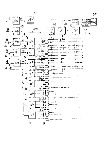
The structure o~ FIG. lC includes fixed-
coefficient multipliers 1-8, AND circuits 9, parity
generator circuits 10, and pipe-line registers 12, 13.
These components are the same as those of FIG. 5.
Furthermore, the configuration comprises a 0 element
decision circuit 11, switch logic gate circuits 14,
15 and 36, and registers 16-18 storing intermediate
values attained by multiplying coefficient input values
of the error location polynomial by location values of
the error location polynomial. Reference numeral 35
indicates an 8-bit fixed symbol generate circuit
generating a binary constant 00000010, whereas reference
numeral 37 designates a pipeline register. The
arithmetic operations are effected in GF (28) and
the number t of errors is assumed to be at most two
in the first embodiment. Referring here FIGs. lA, lB
and lC, description will be given of the operation of
the Galois field arithmetic logic unit constituted as
described above. ~hen the multiplication, division,
and addition are achieved for a syndrome in a Galois
field so as to attain the number of errors and the
value of each coeficient of the error location
~ polynomial, the multiplicatlon is effected such that
: ~ :
~276~4;~
1 when a symbol is inputted as a multiplier, r fixed
coefficients ~ to ~r 1, which respectively are a power
of a primitive element ~ of GF (2r) and a power of (r-l)
thereof, are multiplied in a common fashion, and the each
results are further multiplied by the 0 if each corre-
spondin~ r-order bit of a binary vector of a multiplicand
symbol is 0, and attain an Exclusive-OR of symbols of the
r multiplication results thus obtained, thereby completing
the multipl.ication of a symbol. When the switch logic
gate circuit 15 is changed over to the side of the
input pipeline register 13 of FIG. lC, the Galois field
arithmetic logic unit of this embodiment functions in
a similar fashion as the multiplier circuit of FIG. 5.
The division and addition are to be effected by including
functions of other blocks not shown in this embodiment;
however, such a division can be implemented by combining
a reverse element ROl~ with the multiplier circuit of
this embodiment. After the operations above, the value
; of the coefficient obtained for the each degree of the
error location polynomial is stored in the registers
16-18 by setting the switch logic circuits 14 to the
respective input side ~not to the feedback sides).
The switch logic gate circuits lS respectively change
over be~ween the outputs from the pipeli.ne register 13
storing the multiplicand symbol for the function of
the multiplier. circuit and the outputs from the
registers 16-18 storing feedback values of the inter-
mediate values obtained by assigning the location
- 13 -
43
l value of the error location polynomial for each degree
thereof through a multiplication effected with the
fixed coefficients from ~ to ~2. By changing over
the switch logic gate circuit 14 to the feedback side,
the feedback operation is repetitiously accomplished
as many times as there are steps corresponding to the
code length n. In this operation, the input pipeline
register 13 is supplied with the 0 and all bits of the
input pipeline reyister 12 are set to l so as to suppress
the influence from the terms having a degree equal to
or greater than ~3. This processing is effected at
a quite high speed through a parallel processing and
: : the 0 elernent decision circuit 11 confirms whether or
not the symbol outputted from the parity generator
circuit 37 is a 0 element, thereby judging the root,
which enables to attain the error location represented
as (feedback count + l) in an exponential expression in
the Grois field. Incidentally, since the 0 element
decision circuit ll is located after the fixed-
coefficient multiplier, when the root of the errorlocation polynomial is ~, the root decision cannot
be accomplished by the 0 element decision circuit ll.
In this case, however, since a condition that the
Exclusive-OR of the coefficient of each deyree of the
error location polynomial results in 0 indicates that
the root is ~, the root ~ can be confirmed, for
example, by computing the Exclusive-OR in concurrence
with an operation to store the coefficient values in
- 14 -
1 the registers 16-18. When the root of the error of
location polynomial is determined by the 0 element
decision circuit 11 during the feedback step, the
switch logic gate 36 is changed over to the side of
the fixed-pattern generator 35 before the next feedback
step is initiated. Since the feedback value registers
16-18 are loaded with the respective coefficients of
an expression obtained by assigning the error locations
in the error location polynomial and the fixed-pattern
generator 36 generates a syrnbol containing a binary
value 00000010, the parity generator circuit 10 is
supplied only with a term of degree ~1, The pipeline
register 37 is loaded with the value of an expression
attained by asslgning the error locations in a polynomial
obtained by differentiating the error location
polynomial. By using the value of this expression
in a calculation to be achieved later to attain the
error value, the amount of the computation of the
polynomial can be reduced in the computation of the
error locations. For the simplicity of explanation,
the number of error is at most two in this example.
When the number of error occurrences is particularly
increased and the number of degrees of the error
location polynomial becomes greater, namely, in a
case where the longer period of time is required for
the computation in the conventional method, the effect
of reduction of the computation amount becomes greater.
As described above, according to the embodiment, the
- 15 -
` ~276~
1 subproducts from ~ to ~r 1 obtained from the r
fixed-coefficient multiplier circuits are fed back
to the multiplier circuit of FIG. 5 so as to store
intermediate results for each step in the registers
provided therefor; furthermore, there are additionally
arranged a logic circuit detecting a condition that an
output symbol associated with a parity in the bit
direction is a 0 element, a logic circuit generating
a fixed symbol, and a logic circuit to change over among
functions including an ordinary multiplication, a
computation of a root of the error location olynomial,
and a computation of a value of a polynomial resulted
from a differentiation of the error location polynomial,
thereby simultaneously implementing an efficient
utilization and a high-speed operation of the hardware
resource.
Incidentally, the registers 16-18 as memory
elements in the first embodiment of the present invention
need not be dedicated ones, namely, memories to be used
in a process calculating the coefficients of the error
location polynomial may be employed; furthermore, the
feedback value need not be effected to the same area in
the process calculating the root of the error location
polynomial.
Next, referring to the drawings, description
will be given of a second embodiment of the present
invention. FIG. 2C is a block diagram showing a Galois
arithmetic logic unit as a second embodiment according
- 16 -
~76~3
1 to the present invention. The configuration of FIG. 2
includes fixed-coefficient multipliers 1-8, AND circuits
9, parity generator circuits 10, and pipeline registers
12, 13. These components are the same as those of
FIG. 5. The system further includes a 0 element
decision circuit 11, s~itch logic gate circuits 14,
15 and 36, and registers 16-18 to store intermediate
values resulted from multiplication effected between
input coefficient values of the error location polynomial
and the location values thereof for the respective
degrees. These elements are identical to those of
FIG. lC. Reference numerals 19-24 are registers to
store therein intermediate values resulted fro~ multi-
plication effected between input coefficient values of
the error location polynomial and the location values
thereof for the respective degrees, reference numeral
25 designates a fixed-coefficient multiplier having a
fixed coefficient of ~8, reference numeral 26 indicates
a logic switch circuit changing over between the L and H
levels, reference numeral 27 denotes an AND circuit.
Reference numeral 35 is an 8-bit fixed symbol generate
circult to generate a binary constant of 10101010,
whereas reference numeral 37 indicates a pipeline
register. The operations are accomplished in GF (28).
Since the number t of errors is at most eight in the
second embodiment, the number of memory elements are
increased, and because the number n of errors exceeds
r-l, fixed-coefficient multipliers are dedicatedly
/. , .
1 added corresponding to computation for the degrees
equal to or more than r. ~eferring now to FIGs. 2A
2B and 2C, description will be given of a Galois
arithmetic logic unit constituted as described above.
When attaining the number of errors and the value of
the coefficient of each degree of the error location
polynomial, the multiplication in the Galois field is
accomplished in the same fashion as for the case of
FIG. 5; however, the logic switch circuit 26 is set
to the L level to remove the influence from the term
of the multiplier associated with ~8. In this situation,
all outputs from the AND circuit 27 are set to the L
level and hence the output from the multiplier 25
associated with ~8 does not affect the result of the
multiplication. The computation of the error location
polynomial is achieved in the same fashion as for the
case related to FIGs. IA, lB and lC; however, initi-
alization is effected for up to the eight degree at
the maximum for the error location polynomial depending
on the number of errors. In a case where the number
of errors is at most seven, the calculation of the root
of the error location polynomial and the computation
of the value of a polynomial obtained by differentiating
the error location polynomial can be effected without
any problems only through an initialization setting
the 0 element to the content of the register associated
with the unused degree. In this fashion, after the
error locations are determined according to the Chien's
~Z760~3
1 method, the value of an expression attained by differ-
entiating the error location polynomial can be computed
by use of the multiplier circuit again.
In addition, when operating the apparatus as
an ordinary Galois field multiplier, the 0 element may
be assigned to the register 24 in place of the logic
switch circuit 26.
Incidentally, according to the method above,
! the error location ~ cannot be obtained as a feedback
count; consequently, all coefficients of the error
location equation must be EX-OR summed and be compared
with 0, thereby determining the number of error locations
associated with ~.
Next, referring to the drawings, description
lS will be given of a third embodiment according to the
present invention. FIG. 3 is a block diagram showing
a configuration of a Galois field arithmetic logic unit
as a third embodiment according to the present invention
comprising fixed-coefficient multipliers 2-8, parity
generators 10, a 0 element decision circuit 11, pipeline
registers 12 and 13, a switch logic gate circuit 36,
registers 16-24 storing the intermediate values resulted
from multiplications effected between the input values
of coefficients of the error location polynomial and
the location values of the error location polynomial
; corresponding to the respective degrees, a fixed-
coefficient multiplier 25 with a fixed coefficient
of ~ , an 8-blt fixed-symbol generate circuit 35
. .
19
~;~76~3
1 generating a binary constant 10101010, pipeline registers
37 and 41, octul selector 42 and octul EX-OR gates 40.
These elements are identical to those of the second
embodiment. Reference numerals 38 and 39 respectively
designate NAND circuits. The operations are accomplished
in GF (28) and it is assumed that the number t of errors
is at most eight in the third embodiment.
In this embodiment, the operation to set
values of coefficients of a polynomial to the pipeline
registers 16-24 is effected in a method in which the
values are transmitted through a feedback loop passing
the pipeline register 13, the NAND circuits 38, the
multipliers 2-8 and 25, and the NAND circuits 39 in
this order. Employing this method, it is possible to
` 15 respectively eliminate switches located before the
pipeline registers 16-24 and the multipliers 2-80 In
a large-scale integrated circuit, particularly in a
gate array, the cell area of an NAND circuit is smaller
than that of a logic switch circuit, and hence the
present embodiment enables to configure an LSI in a
higher integration
For an operation of an ordinary Galois field
multiplier, following initialization is needed.
1) The pipeline register 12 are first cleared
and selector logic 26 selects L level. As a result,
all outputs from the NAND circuits 39 are set to the
H level.
2) Clocks are supplied to the pipeline registers
- 20 -
lZ76~3
1 16-24 so as to set all outputs from the pipeline
registers 16-24 to the H level.
3) The pipeline registers 12 and 13 are each
~ loaded with a multiplier and a multiplicand, respectively.
: 5 4) The result of the multiplication is attained
in the pipeline register 37.
; Incidentally, according to the curcult above,
: the error locations for ~ and ~1 cannot be obtained
as feedback counts; consequently, the error locations
must be determined in another method. For example, the
error location for ~1 is iudged as follows. That is,
when the coefficients of the error location polynomial
are stored in memory elements through the feedback loop
~:~ : passing multipliers, a second one-symbol input is
; 15 supplied through selector 36, the input having bits
: ~ ; l's corresponding to the respectivè degrees, and the
outputs resulted from the multipliers assoclated with
:~ the respective degrees are:added so as to compare the
result of the addition with 0.
` 20 Assume here the error location equation to
be
~(X) = k2X + klX + ko
Under this condition, the coefficient values
are sequentially stored through the pipeline register
12 and the feedback loops as follows.
25 1) The pipeline registers 12 and 41 are first
cleared and then selector logic 42 selects register 41.
- 21 -
-
~276~43
1 2) Coefficient which corresponds with ko is stored
in the register 16.
Symbol ~ is supplied through the selector 36
in this situation, and ko is stored in the register 16.
3) Coefficien-t which corresponds with kl is
stored in the register 17.
Symbol ~1 is supplied through the selector 36
in this situation, and the pertinent multiplier outputs
k ~
4) Coefficient which corresponds with k2 is
stored in the register 18.
Symbol ~2 i5 supplied through the selector 36
in this situation, and the pertinent multiplier outputs
k2c~.2 .
Consequently, adding the results with EX-OR
gates 40 outputted from thQ multipliers as described in
~` 1), 2), 3) and 4) above, k2~2 ~kl~l+Ko is attained,
namely, the result of computation of ~ (~1) is obtained
at the register 41 output. When the error location
e~ua~ion is of eighth degree, the switch 26 must be
naturally changed over.
As described above, according to the present
invention, many portions of the multipliers consti-
tuting the Galois field arithmetic unit of the code
error check/correct apparatus can be used to achieve
computations attaining the value of a polynomial obtained
by differentlating the error location polynomial, the
computations being effected at a high speed in a
-` ~27~iQ~3
1 simplified fashion. Particularly, when the number of
error occurrences becomes greater and hence the number
of degree of the error location polynomial is increased,
namely, in a case where a longer period of time is
required for the conventional method to effect the
computation, the effect of reducing the amount of
computations is remarkably increased.
As described above, by sharing the hardware
resources, a high-speed decode operation can be
accomplished by means of a minimized hardware, and
hence the decoding operation can be practically achieved
on such recording media having a high raw error rate
as an optical disk requiring a high-speed and high-
performance operations.
~hile the present invention has been described
with reference to the particular illustrative embodi-
ments, it is not restricted by those embodiments but
only by the appended claims. It is to be appreciated
that those skilled in the art can changed and modify
the embodiments without departing from the scope and
spirit of the present invention.
- 23 -