Note: Descriptions are shown in the official language in which they were submitted.
769~3~
Specification
Title of the In~ention
RF Power Control Circuit
Back~round of the Invention
The present invention relates to an RF power
control circuit of a radio communication device and, more
particularly, to an RF power control circuit capable of
controlling its transmission power in an unvoice interval
of a transmission voice input.
Recently, as radio devices have been made compact
and handy, devices driven by a battery have been
increasingly manufactured. One of important factors of a
portable radio device is a service life of a battery. The
service life largely depends on power consumption during
transmission.
In order to reduce power consumption to
effectively use a battery, some control circuits control
such that transmission is performed in only a voice
interval of a transmission voice and transmission power is
reduced or stopped in an unvoice interval, thereby
suppressing power consumption.
In a mobile telephone system used in the ~orth
America or England, a control circuit is used to control
such that a mobile device always maintains proper
transmission power by a command sent from a base station.
-- 1 --
f~ ,g~3~
Fig. 1 shows a typical conventional control
circuit of the latter. In Fig. 1, in accordance with an
n-bit selection signal SEL supplied from a computer 3, a
switching circuit 1 selects one of 2n DC voltages obtained
by dividing a DC voltage applied to a terminal 5 by
resistors 9 and outputs a reference voltage REE for power
control from an output terminal 6.
In order to easily reali~e the above two types of
control circuits, a control signal CSl representing the
presence/absence of a transmission voice and a transmission
power control signal CS2 received by a radio receiver 7
from a base station are processed by software of a computer
3 to be converted into the selection signal SEL. The
switching circuit 1 is controlled by the selection signal
SEL to obtain the reference voltage REF at the output
terminal 6.
The above conventional RF power control circuits,
however, have the following problems.
That is, the control signal CS1 depends on only
the presence/absence of a transmission voice and is
completely independent of the transmission power control
signal CS2 from the base station. For this reason, since
the two independent signals CSl and CS2 must be processed,
a processing amount of the software of the computer 3 is
increased.
In addition, the computer 3 shown in Fig. 1
performs user inter~ace processing, i.e., checks whether a
6~
volume key, a mute key or a conversation end key is
depressed and performs certain processing if any key is
depressed. Then, the computer 3 performs connection
sequence processing for transmitting/receiving signals with
respect to the base station, checks whether a command for
starting a test mode is input, and if the command is input,
performs a test sequence for starting the test mode.
Thereafter, the computer 3 returns to the user interface
processing. This cycle is repeatedly performed, and each
cycle requires several 10 msec. In addition, these
processing programs have priority over other programs and
no interruption can be made. Therefore, the control signal
CSl from a voice/unvoice identifier 4 can be processed only
after the programs are ended (or before the programs are
started). For this reason, in the worst case, the n-bit
selection signal SEL cannot be output before several 10
msec pass. A man, however, can recognize a voice
interruption of 1 msec. That is, if the selection signal
SEL is delayed by several 10 msec, a head of a voice is
cut.
Summar~ of the Invention
The present invention has been made in
consideration of the above situation and has as its object
to provide an RF power control circuit which can reduce a
processing amount of software and can therefore reduce a
processing time so that a head of a voice is not cut.
~ 3 -
~769~3~
In order to achieve the above object of the
present invention, there is provided an RF power control
circuit for dividing a DC voltage by a plurality of
resistors, selecting one of the partial voltages, and using
the selected voltage as a reference voltage, thereby
obtaining a multilevel RF output, comprising first and
second switching circuits, controlled by an identical
selection signal, each for selecting one of the partial
voltages obtained by the resistors and outputting the
selected voltage, and selecting means for selecting one of
outputs from the first and second switching circuits in
accordance with a control signal.
Brief Description of the Drawinqs
Fig. 1 is a block diagram showing a conventional
technique;
Fig. 2 is a block diagram showiny an embodiment
of the present invention; and
Fig. 3 is a block diagram showing another
embodiment of the present in~ention.
Detailed Description of the Preferred Embodiments
Embodiments of the present invention will be
described below with reference to the accompanying
drawings.
Fig. 2 is a block diagram showing an arrangement
of an embodiment of an RF power control circuit according
to the present invention.
~7~98~
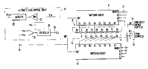
In Fig. 2, each of switching circui-ts 11 and 12
is, for example, a ~PD4051BC (tradename) available from NEC
CORP. Identical 3-bit selection signals SEL are supplied
from a computer (not shown) to terminals A, B and C of the
switching circuit 11 (12) through an input terminal ]3.
The switching circuit ll (12) has eight input terminals X0
to X7 and selects and connects one of the input terminals
X0 to X7 to an output terminal OUT in accordance with the
value of the 3-bit selection signal SEL. When a signal of
low level is supplied to a terminal INHIBIT, the switching
circuit 11 (12) operates; when a signal of high level is
supplied thereto, the switching circuit 11 (12) stops a
selection operation and the output terminal OUT is opened.
A control signal CS1 is supplied from a
voice/unvoice identifier Inot shown) to the terminal
INHIBIT of the switching circuit 11 through an inverter 17
and directly to that of the switching circuit 12. That is,
regardless of the logic level of the control signal CS1, an
operation of either the switching circuit 11 or 12 is
stopped.
A DC voltage applied to a terminal 15 is divided
into partial voltages Vl to V8 bv voltage-dividing
resistors 19. The partial voltages V1, V2,... V8 are
applied to the input terminals X7, X6,... X0 of the
switching circuit 11, respectively. The voltages V3, V4,
V5, V6 and V7 are applied to the input terminals X7, X6,
X5, X4 and X3 of the switching circuit 12, respectively.
-- 5 --
~t769~3~
The voltage V8 is applied to the input terminals X2, Xl and
X0 of the switching circuit 12.
The output terminals OUT of the switching
circuits 11 and 12 are connected to a common output
terminal 16. A reference voltage REF from the output
terminal 16 is applied as a control signal to an automatic
level control (ALC~ circuit 10.
The ALC circuit 10 may be a circuit which is
conventionally used. Generally, the level of an RF input
signal RFIN supplied to an amplifier 21 varies in
accordance with fluctuations in a power source voltage, a
temperature or a difference between individual devices.
Therefore, the level of an output voltage RFoUT detected by
a detector 22 for detecting an output rom the amplifier 21
varies. In order to prevent this variation, the output
detected by the detector 22 is supplied to a differential
amplifier 23. The reference voltage REF selected and
output from the switching circuit 11 or lZ is supplied as a
reference voltage to the differential amplifier 23. An
output from the differential amplifier 23 is supplied to a
controller 24~ The controller 24 controls an input voltage
Vcc from a terminal 25 in accordance with the output
voltage from the differential amplifier 23, thereby
controlling the gain of the amplifier 22. As described
above, the ALC circuit 10 constitutes a loop circuit for
m~intaining the output level of the amplifier 21.
An operation of the circuit shown in Fig. 2 will
be described below.
Assume that the 3-bit selection signal SEL is
(1,0,1) and the switching circuits 11 and 12 select the
input terminals X5. Therefore, the switching circuits 11
and 12 connect the voltages V3 and V5 to their output
terminals OUT, respectively.
In addition, assume that the control signal CS1
goes to high level if a transmission voice is present. In
this case, since the terminal INHIBIT of the switching
circuit 12 goes to high level, an impedance at the terminal
OUT is increased. Meanwhile, since the terminal INHIBIT of
the switching circuit 11 goes to low level, the output from
the switching circuit 11, i.e., the voltage V3 is obtained
as the reference voltage REF at the terminal 16.
When a transmission voice becomes absent, the
logic of the control signal CSl is inverted, and therefore
an impedance at the terminal OUT of the switching circuit
11 is increased. As a result, the voltage V5 of the
switching circuit 12 is obtained as the reference voltage
REF. Transmission power of the ALC circuit 10 of the radio
communication device is controlled by this reference
voltage REF.
In the above embodiment, the analog
switches ~PD4051 (tradename) each for selecting one of
eight voltages in accordance with the 3-bit selection
signal are used as the switching circuits 11 and 12. The
~.,c~769~
present invention is, however, not limited to the above
embodiment, but any switching circuit for selecting one of
2n input voltages by an n-bit selection signal may be used.
In this case, the circuit may be arranged such that a
voltage Vm (1 < m c 2n) is applied to each input terminal
of the switching circuit corresponding to transmission
power generated when a voice is present and a voltage Vm k
(1 ~ m - k ~ 2n) i5 applied to each input terminal of the
switching circuit corresponding to transmission power
generated when no voice is present.
Fig. 3 is a block diagram showing another
embodiment of the present invention.
In Fig. 3, switching circuits 31 and 32 are not
inhibited but always operated by a selection signal SEL.
lS A control signal CSl representing VOICE/UNVOICE
is supplied to a terminal A of a switching circuit 37.
The switching circuit 37 connects an input
terminal X0 or Xl with an output terminal OUT in accordance
with a signal supplied to the terminal A.
As has been described above, according to the
present invention, a power control processing amount of
software can be reduced and accordingly a processing time
can be reduced, thereby realizing high-speed RF power
control.