Note: Descriptions are shown in the official language in which they were submitted.
~77~29
--1--
This invention relates to substrates which include
~ilamentary members and which support and interconnect
components, a method for making such substrates, apparatus for
carrying out the method and to the substrates produced
thereby.
U.S Patent Nos. 3,674,602 and 3,674,914 both dated
July 4, 1972 and applicant's Canadian Patent No. 1,102,924,
issued June 9, 1981, disclose and describe circuit boards
employing filamentary members of wire, and methods and
apparatus for making such boards. In such disclosures and
descriptions, a wire is scribed onto the energy activatable
surface of an insulated base or board. The wire is scribed
onto the surface in a predetermined pattern with a head. The
head is energized, activates the surface as the wire is
brought into contact therewith and bonds the wire to the board
of base surface. The movement of the board, head and wire and
energizing of the head are controlled in such fashion that the
wire is scribed and fixed to the board in a precise pattern.
In recent years, new techniques for electronic
packaging using wire scribed and printed circuit boards have
reduced the size and weight of electronic equipment. Further
reductions have been achieved through the development and
general availability of integrated circuits incorporated into
a microelectronic package. Such packages, commonly called
dual-in-line packages, embody leads through which electrical
rn/~
~k
~ ~77429
1 contact may he made with the integrated circuit and which also
2 serve to mount and connect the package to the holes in the wire
3 scribed or printed circuit board.
Extrelnely ~ompact microelectron1c packages have been
developed to accommodate these complex integrated circuits.
6 One such fa~ily of packages, commonly called chip carriers, may
7 be surface mounted ratller than being connected by leads passing
8 througll the board. These packages are square and have
9 ¦ terminals on all four edges rather than on two sides as in the
lO ~ dual-in-line packages. The terminals are spaced on centers of .
11 1 50 mils, 40 mils or less, thus substantially reducing the area
12 of the package as compared to the dual-in-line package. This
13 substanti.ally increases the number of terminals per Ullit area. .
14 The reduction in package area made possible by the :
chip carrier substantially increases the num'oer of
16 microelectronic packages which may be mounted and electrically
17 connected by a circuit board or interconnection substrate of
18 given area.
].9 I-lowever, such increase in number of packages or
component pac}cage density and closer terminal spacing increases
21 the terminal density requirement on the board or substrate and
22 the heat density of the system. This increased terminal
23 ¦ density generates and re~uires higher conductor-density.
24 ! Contact pads, rather than through holes, are employed on the
surface of the substrate to provide higher conductor density.
26 Electrical contact between such surface pads and the substrate
Z7 conductors can be made in dimensions which approach that of the 1-
28 ¦ conductor itself.
29 A process for scribing filaments onto a carrier in a ':
predetermined pattern in a high de~sity horizontal and vertical ¦
~2~429
--3--
grid is known and described in U.S. Pa~ent No. 4,500,389. The
filaments are applied or scribed to the carrier in a predeter-
mined pattern with apparatus such as that shown and described
in the aforementioned Canadian Patent No. 1,102,924 or U.S.
Patent Nos. 3,674,602 and 3,674,914. The filaments may be
optical f ibers or preinsulated wires, such as copper wire of
ahout 2 to 4 mil dia~eter. Thug, the filaments contain at
least one conductive portion i . e ., a portion Which can act as
a conductor, e.g., an electrical conductor, an optical conduc-
tor or the like. The conductive portion of the filaments may
or may not have a dielectri~ Coating. The filament~ are
bonded to the carrier in a high aen~ity horizontal an~ ver-
tical grid. A layer of Coating material capable of being
hardened at a temperature below 100C is applied over the
filaments forming a smooth, planar surface over the carrier
and filaments~ The coating material iB then cured. The
carrier is attached to a table movable in a controllea pattern
along 'X' and 'Y' axe8 So a to locate preprogrammed points on
the carrier under a high energy beam, such as a coherent laser
(e.g. CO2 or other suitable laser), controlled depth mechanic-
al drills, a modulated stream of abrasive particles, a water
jet or stream of chemicals or solvents.
The beam is directed perpendicular to the table and
to the carrier mounted thereon. Alternatively, the carrier
may be fixed and the beam moved in 'X' and 'Y' axes. The
location of the filaments in the hardened, planar material are
targeted optically so as to subs~antially eliminate location
errors. The carrier is moved relative to the high energy beam
so that the desired filament is in line with the beam at a
rn/rm
-- lZ'77429~
-I `
ll . ,.'
i ,`,
1 predetermined point. The filament i5 then exposed by the beam
2 at such point. If the filament is metallic, a high energy
3 ~eam, such as A C02 laser is used. The beam iS aligned with
the desired predetermined point on the filament, and then the
beam is pulsed or modulated to direct energy at the filament so
6 as to vaporize and remove the hardened material and the
7 filament insulation, leaving a precisely formed cavity with the
8 filament substantially exposed.
9 Even greater density and better electronic properties
can be achieved using the improved processes for making
ll interconnection substrates set forth herein. The improved
12 processes of this invention enable the production of
13 interconnection substrate which can accommodate high pin-count, I
l~ high-speed electronic packages. The improved processes of this ¦~
inve11tio11 afford the electronics industry new ways in which to
l~ construct high-density interconnection circuits.
17 According to the process of this invention, the ¦,
18 material which forms the core of the substrate base used in the
]9 present invention should be made from materials which have good .
heat dissipation properties, which are dimensionally stable
21 (i.e. do not exhibit net dimensional change after experiencing
22 -temperature excursions) and which have coefficients of thermal
23 expansion in the X-,Y-plane which match the coefficient of
24 thermal-expansion of the chip carrier or integrated circuit
materials to be mounted on the substrate.
26 Another improvement over known processes is the
27 sequential layering of circuit patterns which provide circuitry
28 for two or more functions on one interconnection circuit
29 board. Still another improvement is a process providing means
for wiring a substrate base on both sides and providing-- -
~ ~Z~77~29
~! 1 side-to-side communications.
2 The present invention will be more fully described and
~ 3 will be better understood from the following further
., 4 description of preferred embodiments of the in~ention taken
with the appended drawings in which:
Figure 1 is a perspective view with partial cut-away
7 of an interconnection substrate made according to the processes
8 of this invention having a multiple-layer substrate core and
9 plated through hole communication between both sides of the
boards.
11 Figure 2 is a cross-sec-tional view of an
12 interconnection circuit board having multiple levels of power
13 and ground planes.
14
DETAILED DESCRIPTION OF TIIE PREFERRED EMsoDIMENTs
16
1~ In the instant invention, a high density
18 interconIlection circuit may be formed and processed on a
].9 substrate core which will form an integral part of the
~0 article. Therefore, said substrate core must selected from a
21 group of materials which are suitable for incorporation into
22 said high density interconnection circuit, and which are
dimensionally stable for the process to be employed in its ;
24 fabrication.
25 ¦ Preferably, the substrate core may be made of an alloy
26 of nickel and iron, preferably between 55-65% iron and 35-35%
27 nickel. More preferably, an alloy of about 57-60% iron and
28 40-43~ nickel should be used. The alloy sheet is preferably
29 clad with a thin layer of conductive metal such as copper to .
provide thermal and electrical conductivity. The core may also
~ _ 5 _
~774::9
.,
:i `,,
1 be a thin laminate composed of a thin fiberglass-reinforced
2 epoxy resin sheet bonded on both sides with composite metal ~
3 sheets. The composite sheets tllemselves should have thin metal .
4 alloy cores of about 60-65% iron and 35-40% nickel which are
clad with very thin copper sheets. Also preferable for use as
6 1 core materials are copper/molybdenum alloys, pol~imides and
7 epoxy resins which may be reinforced with glass, quart~,
8 Kevlar~ or the like. Preferably, the coefficients of thermal
9 expansion should be between 5 and 20 x 10-C in/in/C. Some
examples of possible core materials and their coefficients of
11 thermal expansion in the X,Y-plane are shown in Table I. :
12
1~ TABLE I
14 TYPICAL THERMAL C0EFFICIENTS OF EXPANSION (ln X-- and Y- Axes)
16 FOR SEVERAL COMMONLY USED SU~STRATE CORE MATERIALS
17 SUBSTRATE TYPE TCE
Alloy 42 (58~ iron, 42% nickel 5.5 X 10 in/in/C
18 Cu-clad Invar (64% iron, 36~ nickel) 5-8 X 10-' in/in/C
Cu/Mo Alloy 6.0 X 10-C in/in/C
]9 Polyimide/~uartz 7-9 X 10-~ in/in/C
Polyimide/Glass 12 X 10-C in/inJC
20 Polyimide/Kevlar R 5-7 X 10-C in/in/C
Epoxy/Kevlar ~ 5-7 X 10-C in/in/C
21 Epoxy/Glass 12-16 X 10-~ in/in/~C
22
23 If leaded components are utilized, however, the
24 ¦¦ coefficients of thermal expansion of the substrate core and the
25 ¦ components need not match.
26 The present invention may be used to make particular
27 interconnection circuit boards having the ability to
28 accommodate compact microelectronic packages. The
29 interconnection circuit boards made according to the present
invention may take the form of certain preferred embodiments. ¦
!~
' - -6- 1i'
~ r~ 1277429 : ¦~
l One preferred process of makinc1 the interconnection
2 circuit boards according to the present invention is to apply
3 thin copper foil to each side of a substrate core using a
4 suitable dielectric bonding material. CirCuit patterns should
be formed on one or both of the copper foil surfaces according
6 to methods known to those possessing skill in the art. The l :
7 substrate base should be treated so as to promote adhesion.
8 The surface of the substrate base should then be encapsulated
9 with a resin so as to obtain a flat, smooth, planar surface. I
].0 The coating should be covered with an adhesive and the surface
11 s~ribed wi~h filaments, such as wire conducto~s. The formed :
12 wire-scribed circuit pattern should then be encapsulated with .
13 resin to form a s~ooth, flat, planar surface and to provide a
1~ means ~or maintaining the positional relationship of the
15 filaments. It should then be further coated with adhesive. i
16 This substrate should be mounted on an X-, Y- positioning table
17 and cavities formed at predetermined locations. Thelcavities
18 should be cleaned and treated to promote subsequent metal
]9 plating. The substrate should then be plated with conductive
20 material and circuit patterns should be formed in the :
21 conductive material according to methods known to those of
22 ordinary skill in the art. -
23 In another preferred embodiment, a sequence of layers
24 may be produced which provide circuitry for two or more desired l
25 functions on one board. In this embodiment, conductive ! :
26 I material should first be laminated to a substrate core using a l :
27 dielectric bonding material. A circuit pattern should be i
28 formed on the resulting substrate base. The surfaces should be
29 treated to promote adhesion. Thin sheets of conductive
30 ¦ m erial should be laminated to the base such that the
- 7 -
,.,. , , . ., ~ I 1-
~r 1277~29 -
l conductive material is isolated from the base and is on the ;
2 exterior surfaces. Additional circuit patterns can then be :
3 formed on`the conductlve material. The substrate base should -
4 then be placed on an x-, Y- positioning table for cavity
formation between the two conductive layers in predetermined ¦ .
6 areas between the two conductor layers. The substrate base
7 should then be plated to deposit conductive metal in the.
8 cavities. If desired, additional circuit layers may be formed
9 over these layers in accordance with the process of this I
1.0 invention. The surface of -the su~strate base should be ,
ll encapsulated with a resin so as to obtain a flat, smooth, .
12 planar surface. The coating should be covered with an adhesive
13 and the surface scribed with filaments, such as wire .
14 conductors. The wire-scribed circuit pattern should then be :
encapsulated with resin to form a smooth, flat, planar surface .
16 and to provide a means for maintaining the positional
17 relationship of the filaments. It should then be further
18 coated with adhesive. This substrate should be mounted on an
]9 X-, Y- positioning -table and cavities formed at predetermined
~0 locAtiol1s. The cavities should be cleaned and treated to .
21 promote subsequent metal plating. The substrate should then be
22 plated with conductive material and circuit patterns should be :
23 formed in the conductive material according to methods known to
24 those of ordinary skill in the art. This embodiment provides
for at least two circuit levels, which can be used for power
26 and ground distribution, logical functions, or the like.
27 Obviously, more than two or three circuit levels built on the
28 substrate base.
29 Using the encapsulating method of the present
30 1 invention in order to maintain the position of the wires and
:
l4ir 1277429
, ~i ,
1 thus enable the conductors to be scribed in high density,
Z anotller er~odiment may be produced. The substrate base may be
3 wired oll both sides and prov;ded with plated through-holes in ..
order to provide side-to-side con~nunications between the sides
5 of the circuit board. The conductors should be positionally .
6 stabilized with an encapsulation layer according to the present i
7 invention to enable very close clea~ances. In this embodiment,
8 one or more cavities may be made in addition to the
9 through-holes. .
10 In the preferred embodiments of the invention, the
11 dielectric substrate base is mounted on and affixed to a rigid
12 stable base while the wire is scribed, the liquid coating is
1~ ¦ applied, leveled, flattened and cured in accordance with the
14 with the teachings of the ~.S. Patent No. 3,607,380 dated c
15 September ~1, 1971. The CaYities in the circuit which are used :i,
16 to expose the wires or conductors are formed by high energy ¦1
17 beams and the holes are electrolessly plated or electroplated.
18 In the preferred embodiments of the invention, the l
]9 conductor or wire extends through the high-energy-formed cavity .
at the time of plating. This provides better electrical
2l contact and mechanical strength between the conductor and i
22 cavity plating metal than could be provided when attempting to
23 drill through a 2 to 4 mil diameter wire with a 6-12 mil ;
24 diameter drill. .
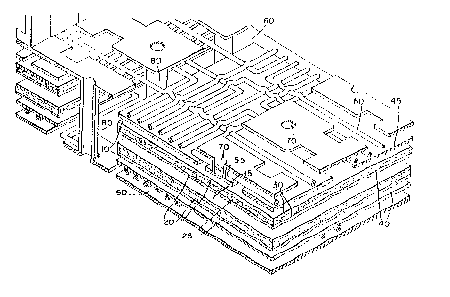
Figure 1 is a perspective view with partial cut-away
26 depictillg an improved interconnection circuit board made in
27 accordance with the processes o~ this invention. Figure 1
28 ¦ depicts the substrate base 10 which is also described in
29 1 Example 4, below. The substrate core lS is an epoxy reSin ~
30 ~ sheet, The epo~y reSin sheet core 15 is bonded on each side by ¦ i
.,; .,... -9- ..!.: ~
-- :::
~;lr ~2~7429
'i`
: i
1 composite metal sheets 30 consisting of very thin metal alloy .
2 cor~s 25 and cladding 20. Cores 25 are alloys of 64~ iron and
3 36~ nickel. sOth sides of cores 25 ar~ clad with copper ,
4 cladding 20. '
A layer of ~lat planar coating 40 is placed over
6 cladding 20. Over this coating layer 40 is laid a conductive
7 copper l.aminated sheet 45 is applied to both sides of the
8 structure. This copper sheet 45 is etched and wire filaments
~ 50 are scribed in a predetermined pattern onto both sides of .
10 the base s-tructure. A smooth, flat, planar coating 60 is :
11 applied over filaments 50. Cavities 70 are made by exposing ! -:
12 predetermined points along the base structure to a C02 laser ~ :
1~ and oblating the smooth, flat planar coating at those points, i `
14 This procedure leaves the filaments 55 intact. At other
predetermined points, holes 80 are drilled to afford
16 co~munication between both sides of the interconnection circuit
17 board. ¦ I
18 Figure 2 is a cross-sectional view of an improved
].9 interconllection circuit board made in accordance with the
process of this invention. A substrate core 110 is laminated ¦ :
21 with Copper foil 115 and an epoxy resin sheet 120. ¦ .
22 A circuit pattern 125 is formed on the surface of ¦ :
23 epoxy resin slleet 120 to form the power level. The exposed .
24 copper metal is etched on the surface of base encapsulated with
25 a smooth, flat, planar coating 130. This coating is cured and ¦~
26 ¦ circuit patterns are formed on the surface of Coating 130.
27 ¦ Copper metal is dissolved and removed from desired areas 140.
28 ¦ l}le substra-te base is then placed on a numerically-controlled
29 ¦ X-, Y- positioning table and the -table moved to predetermined
30 1 locations. Such locations 135 are exposed to a CO~ laser,
. .
-10-
~ . .'~ ~Jl'
Z77429 1 1
l ~
i l.~
1 whicll orrns a cavity at each location. The substrate surface
2 is then electroplated to deposit metal in cavities 135. This
3 level is the ground level. The substrate base is then
4 ellcapsulated with a layer of resin 150 and wire filaments 160
are scribed onto the surface of resin layer 150 in a
6 predetermined pattern. Filaments 160 are encapsulated with a .
7 smooth, flat, planar surface 170. Cavities 180 are formed in
8 predetermined locations using a C02 laser. The Cavities are ;
9 ¦ metallized in this embodiment, access is provided between power
level 125 and the external surface of the board by means of
11 power cavity 185. The metallization of power cavity 185 i
12 contacts the metallized ground layer 138 which itself contacts ¦
13 power level 125. Likewise, the metallization of ground cavity
1~ 188 contacts ground level 136. This structure,permits the i
15 board to accommodate a multiplicity of functions. 7.'
16 In the practice of the instant invention cavity ~
17 forming ~ith a high energy beam, such as a laser, has been ~;
18 found to be particularly useful. However, as already noted, ~
19 other means, sUch as a driIl bit, abrasive, chemical or high ~:
20 speed jet might also be employed. Other high energy beams g
21 absorbable by the material being drilled, but not the conductor i
22 or wire, and capable of volatilizing the material and ~:
23 insulation on the conductor or wire, may be employed. ¦
24 The following examples serve to illustrate certain ¦
25 preferred embodiments of the present invention. The purpose is
26 ;~ not, in any ay, to limit the scope of the present Invention.
3g
l . .
;''i;"" - 11-
'~; ' . !, , ."" ~ ~
lZ77429 11
1 EXAMPLE 1
2 l l ,
3 A 0 . 018-illCIl thick metal alloy sheet core of 64~ iron -
4 and ~6% nickel was clad on both of its planar surfaces with .
S copper ~etal sheets having a thickness of 0.006 inch. The ll
6 copper surfaces were treated witl- black oxide solution to .
7 promote adhesion. The substrate base was laminated on each
8 side with copper foil 0.0014 inches in thickness and a
9 semi-cured fiberglass-reinforced epoxy resin sheet. The
lamination took place at a pressure of 375 psi and 350F for a
11 period of 25 minutes. The substrate base was then baked at a
12 temperature of 350F for 1 hour in order to effect full curing
13 of the epoxy resin.
lb The substrate base was then brushed in order to clean ':
15 ¦ the surface. Circuit pat-terns were formed on one side of the !l -
16 I substrate base by exposing a dry film photoresist to an ¦'
17 i ultraviolet light source and developlng the pattern. The other ,
18 I side of the substrate hase was encapsulated by photoresist
]9 ¦ material.
The substrate base was then exposed to a ferric
21 chloride-water solution to remove exposed copper metal from the .
22 surface of the subs-trate base. The remaining photoresist was . .
~3 removed from the surface and the substrate base treated with
24 black oxide solution to promote adhesion.
The patterned surface was then coated with an
26 encapsulating resin according to the following procedure:
27 A pair of rigid rollers, mounted parallel to each l ,
28 other, were adjusted to provide a controlled encapsulation ! .
29 thickness. A filled, thermosetting epQxy resin which cures at
¦ room temperature was thoroughly mixed with an amount of curing
I . .
. - 12 ~ ~ ~
~ ~~
. ,, . . -
lZ774L29 ~ ~
1 agent sufficient -to ensure complete polymerization o~ the .
2 system. This mixture was placed into a bell jar and the bell
3 jar evacuated with a vacuum pwnp. The mixture was uniformly .
4 applied to the patterned surface of the substrate base. The : :
substrate base was then placed in a vacuum chamber t~ remove
6 any air in the mixture. After removal from the vacuum chamber,
7 one edge o f the substrate base was placed into the preset gap
8 between the rigid rollers. One end of a 0.004-inch thick
9 release-treated polyester carrier sheet on which was coated a .
10 0.0027-inch thick sheet of wiring adhesive was placed in ;
ll contact with and parallel to the gap edge of the substrate
12 base. The substrate base, carrier sheet and adhesive were then
13 drawn through the gap in order to bond the adhesive to the
14 resin surface such that the surface of the adhesive was
15 substantially flat. ¦i
16 The encapsulating resin was allowed to cure at r~om ¦'-
17 temperature for a period of 8 hours. The suhstrate base was I.
18 then baked for period of 30 minutes at a temperatUre of 150F.
19 After baking, the substrate base was placed onto a .
20 computer-controlled X-, Y- positioning table with the .
21 adhesive-coated surface e~posed. An energized wiring head
22 assembly was brought into close proximity with the adhesive .
23 surface and an insulated copper wire 0.0025 inch in diameter .
24 was placed between the head assembly and the adhesive surface,
The table was moved to predetermined locations and the head
26 assembly was directed to dispense the insulated wire and toa. ¦
27 bond it to the adhesive surface and thereby form a precise.: ~!~28 wire-scribed circuit pattern. The substrate base was then l
29 baked for a period of 90 minutes at a temperature of 200F. l
The wire scribed circuit pattern was then coated with .
77429 1 ~;
1 an encapsulating resin coating and adhesive sheet to stabilize
2 the posi~ion of tlle scribed wire and to form a flat, planar
3 surface in accordance witl- the procedure descr;bed above. The ~-
4 adhesive sheet ln this procedure was specifically-adapted for . .
processing using semi-additive plating techniques. This
6 adhesive sheet was 0.0012 inch thick. After 'oeing drawn
7 through the rollers, the substrate base was allowed to cure at
8 room temperature for 8 hours and then baked at 150F for 90
9 minutes.
The substrate base was then placed onto an X-, Y-
11 positioning table with the adhesive surface exposed and the
12 beam of a carbon dioxide laser was directed at the adhesive
13 sur~ace at predetermined locations. The laser beam vaporized
14 and removed the materials surrounding the copper wire, and
15 formed cavities which were between O.OlO and 0.012 inch in ,
16 diameter. ,;
17 The substrate base was then placed in an oven and .~
18 baked for 30 minutes at a temperature of 250F. The i j
19 temperature of the oven was then increased to 350F and the
substrate base was baked for an additional 90 m;nutes. The i
21 substrate base was cleaned by an ultrasonically-agitated
22 cleaning solution and rinsed in order to remo~-e any dirt or
23 debris from the laser-generated cavities. The substrate base I
24 and cavities were further cleaned by immersion for forty 1:
minutes in a solution of potassium permanganate in water which
26 was maintained at a pH of about 13.5. After this immersion,
27 I the substrate base was immersed for 3 minutes in a permanganate
28 neutralization solution of stannous chloride and'hydrochloric i
29 acid in water. This solution was maintained at room 1
temperature. Immediately t]~ereafter, the substrate base was ¦
. - 14 - j -
!
_-~,~
~f~ ~'77429
1 immersed in a second neutrali~ation solution having a reduced -
2 stannous chloride concentration for three minutes. The ,
3 substrate base was rinsed in running water for 6 minutes. '
ll A palladium/tin catalyst was applied to the substrate
base to activate it. It was then immersed in an electroless
copper plating solution of the type commonly used for the
~ ¦ manufacture of printed circuits until a very thin layer of ¦
8 copper metal had been deposited on its surface. It was removed
9 from the electroless copper plating solution and rinsed in
10 running water for 60 seconds. The substrate base was then
ll electroplated to increase the thickness of its surface copper
12 deposit.
13 ¦ The substrate base was then brushed and coated with a
14 ¦ dry film photoresist which was exposed and developed as
lS described above to form a circuit pattern on the substrate
16 base. It was then again electroplated in order to increase the
17 thickness of the copper deposit in those areas which had been ¦~
18 exposed by patterning the photoresist. The substrate base was
]9 rinsed in running water and immersed in a commercially
~0 available tin/lead electroplating solution in order to deposit l,
21 tin/lead on all exposed copper surfaces.- ;
22 The photoresist was removed from the surfaces of the .
23 substrate base and then exposed to a copper etching solution
24 which did not dissolve or remove the tin/lead plating,
preserving the desired circuit pattern while all undesired
26 copper metal was dissolved and removèd.
27 The substrate base was rinsed in running water and
28 then baked for 30 minutes at 150F. The tempe~ature was
29 ~ increased to 350F and the substrate base baked for an
~0 ~ additional 120 minutes. The substrate base was then sub;ected
. i ' .
i
,,' ~ 15 ~
.
_ _r.~~r ~
4;~9 ~;~
1 ~ to collventi ~a1 fabrication operations such as cuttlng to size,
Z and drilling m~unting holes to produce a finished wire-scrlbed
3 circuit board.
4 1 ,
EXAMPLE 2 .
7 .~ 0.01~-inch thick metal alloy sheet core of 64~ iron
8 and 36% nickel was clad on both of its planar surfaces with
9 copp~r metal sheets having a thickness of 0.006 inch. The
0 copper surfaces were treated with black oxide so1ution to
11 ¦ promote adhesion. The substrate base was laminated on each
12 side with copper foil 0.0014 inches in thickness and a
13 semi-cured fiberglass-reinforced epoxy resin sheet. The .
1~, lamillAtion took place at a pressure of 375 psi and 350F for a
15 ! period of 25 minutes. The substrate base was then baked at a .
16 temperature of 350F for 1 hour in order to effect full curing ,
17 of the epoxy resin. . l ~
18 The substrate base was then brushed in order to clean l :
]9 the surface. Circuit patterns were formed on one side of the
substrate base by exposing a dry film photoresist to an ,
21 ultraviolet light source and developing the pattern. The other
22 side of the substrate base was encapsulated by photoresist ¦
23 material.
24 The substrate base was then exposed to a ferric
chloride-water solution to remove exposed copper metal from the
26 surface of the substrate base. The remaining photoresist was
27 removed from the surface and the substrate base treated with l ~
28 black oxide solution to promote adhesion. , ;
29 Rfter patterning, thin, single-sided copper-clad
laminated sheets were applied to each side of the substrate ~
; .'
- 16 -
.,; . : ` . !
- ~
., ~27742~
1 base laminating semi-cured fiberglass reinforced epoxy sheets
2 as the bonding med~um as in Example 1. The substrate base was
3 then baked in order to cure the epoxy resin fully. ;
4 Circuit patterns were formed on the substrate base as
described above in Example 1, except they were in the form of
6 circular areas which were between 0.008 and o.olo inch in
7 diameter. The copper metal was dissolved and removed from the :
8 circular areas, and the photoresist was removed as in Example 1.
9 The substrate base was then placed onto la
computer-controlled X-, Y- positioning table with the circular
11 areas exposed. The table was moved to predetermined locations
12 in order to vaporize and remove the cured epoxy resin layer
13 between the two copper layers in the circular areas using a
14 carbon dioxide laser as in Example 1. .
15 The substrate base was then cleaned and rinsed as l :
16 described in Example 1. The substrate base was then activated , .
17 using a palladium/tin catalyst. It was immersed in an acidic :
18 copper sulfate plating solution and electroplated to deposit
19 copper metal in the cavities. After this plating operation;
~0 the substrate base was removed from the solution, rinsed in . .
21 runliing water for 2 minutes and dried. .
22 The substrate base was then encapsulated, wired and
23 processed in accordance with Example 1. .
24
2S EXAMPLE 3
26 .
27 The procedures of Example 1 were followed except that
28 the metal alloy sheet used as the core was composed of 59% iron
29 and 42~ nickel, and it was not clad with copper metal sheets. .
30 Mechanical roughening techniques were employed in order to .
. . .
. .: - 17 - .'
Y' ~
~LZ7~29
1 promote adhe 6 i on .
3 EXAMPLE 4 :
. ~
S The procedures of Example 2 were followed except that .
6 the metal alloy core was replaced by a thin laminate consisting
of a o.oos-inch thick fiberglass reinforced epoxy resin sheet
8 bonded on each side with composite metal sheets. These ¦
9 composi~e metal sheets considered o 0.0045-inch thick metal
alloy cores (64~ iron and 36% nickel) both sides of which were
11 clad with 0 00075-inch thick copper metal.
12
13 RXAMPLE 5
14 l
15 A metal alloy core of 64~ iron and 36~ nickel and
16 which was 0.006 inch thick was clad on each surface with copper
17 metal sheets having a thickness of 0.002 inch. This metal ;
18 alloy core was placed onto an X-, Y- positioning table, the
19 table was moved to predetermined locations, and 0.042-inch
~0 diameter holes were mechanically drilled through the core.
21 . The copper surfaces of the drilled metal alloy sheet
22 were treated to promote adhesion through the use of a ,
23 commercially available black oxide treatment solution.
2~ Several sheets of semi-cured fiberglass reinforced
epo~y resin were used to f ill drilled holes in the core, and a
26 sheet of copper foil 0.0014 inch thick was laminated to one
27 side of the drilled metal alloy core as described in Example 1. 1 :
28 Another sheet of copper foil 0.0014 inch thick was
29 then laminated to tlle other side of the drilled metal alloy
core in the same manner. After application of the copper foil
. . ,~
, .. ` ~ 18 -
~ r~
~;'r''~ '~ lZ77A29 7'
.
.~ ,~
1 to each side of the drilled metal alloy core,lthe resulting
2 subs-trate base was baked for 60 minutes at a temperature o~
3 a50OF to full~ cure the epoxy resin.
4 The substrate base was then brushed in order to remove
dirt, dust, oxide and similar foreign material from the surface
6 of the copper foil. A dry film photoresist was then applied to
7 each side of the substra-te base in order to form circuit
8 patterns on each side of the substrate base.
9 The substrate base was then exposed to ferric chloride
0 solution as described in Example 1 to dissolve exposed copper
11 metal. The remaining photoresist material was removed and the '.
12 copper exposed to black oxide.
13 The substrate base waS then encapsulated With reSin
14 and adhesive and scribed with wire, one side at a time,
15 according to the procedures of Example 1. ¦
16 The substrate base was then baked for 30 minutes at
1.7 250F. The baking temperature was then increased to 350F and
18 the substrate base baked for an additional so minutes.
19 The substrate base was then placed onto the X-, Y-
positioning table described above, the table was moved to the
21 same locations in which holes were drilled earlier, and 0.020
22 inch diameter holes were mechanically drilled through the .
23 layers on the substrate base.
24 The substrate base was then subjected to the
cleaning/adhesion promotion treatment and plated in accordance
26 with the process described in Example 1, above.
27 The terms and expressions which have been employed are
28 used in terms of description and not of limitatioll, and there
29 is no intention, in the use of such terms and expressions, of
excluding any equivalents of the features shown and described
!"~; e' . ~;
~277429
1 or portions thereof, but it is recogni~ed that various ..
2 modifications are possible within the scope of the invention
cl~im~.
19
22
24 . .
26
27 .
28