Note: Descriptions are shown in the official language in which they were submitted.
SELECmIVE INTERMIXI~IG OF LAYERED STRUCTURES
COMPOSED OF T~IN SOLID FILMS
DESCRIPTION OF THE INVENTION
TECHNICAL FIELD
This invention relates to synthetic layered semi-
conductor structu~es and their modification, both laterally
1~ and vertically, to provide no~el electronic optoelectronic,
and optical properties. This is accomplished by selective
intermixing o~ such layered structures through selective
irradiation with laser beam or electron beam energy sources
to effect reaction between adjacent layers to a depth
dependent on the energy density.
B~CKGROUND ART
A particular class of synthetic layered structures
of considerable importance is the semiconductor superlattice
in which two semiconductor materials with different elec-
tronic properties are interleaved in thin layers either (1)
by depositing sheets of two semiconducting materials in an
alternating manner, or (2) by introducing impurities into
layers of a single semiconducting material. The former is
designated as a compositional, or heterostructure, super-
lattice, and the latter is designated as a doping super-
lattice. Thus, a compositional superlattice comprises a
periodic array consisting of alternating layers of two
di~ferent semiconductors. Each layer has a thickness in the
range from a single atomic layer up to several hundred
atomic layers. In a compositional superlattice, the two
semiconductors are so chosen that their band gaps, i.e., the
difference in enerqy between the valence and conduction
bands, differ significantly.
In the literature, a structure composed of two
thin films of different semiconductors is called a single
heterostructure. A structure composed of a semiconductor
film of lower band gap sandwiched between two semiconductor
~77433
layers of larger band gap is referred to as a double hetero-
structure. When the middle layer is sufficiently thin, the
structure is called a single quantum well (SQ~ periodic
structure composed of alternating layers of two different
semiconductors is sometimes also referred to as a multiple-
quantum-well ( MQW) or a superlattice depending on ~he
thickness of the semiconductor layer with the larger ba~d
gap. For the purposes of this invention, the distinction
between a superlattice and a MQW is not essential, and thus
the term "superlattice" will be used henceforth for the sake
of simplicity ~s used herein, it is intended that the term
"selective intermixing" includes also the case where all
regions of a synthetic layered structure are intermixed as
well as the case where only a limited portion thereof is
intermixed.
Specifically, each layer of the semiconductor
having the smaller band gap produces what is referred to as
a potential well in either the conduction band or the
valence band, or in both. In terms of optical and elec-
tronic properties, important distinctions can be made
between three different types of semiconductor super-
lattices, commonly referred as as types of I, I', and II,
depending on the relative alignment of the conduction and
valence bands in the two semiconductors. However, for the
purposes of this invention, such distinctions are not
essential. Inside each potential well, only certain energy
states or levels are available to the confined carriers
(electrons in the conduction-band or holes in the valence-
band)O The values of the energy levels available to theelectrons can be selectively controlled by appropriate
choice of semiconductor materials and the width of their
layers. In this fashion, the electronic and/or optical
properties of SQW's, or of compositional or doping super-
lattices, can be tailored.
It is generally well known in the art that in asemiconductor multilayer structure, the semiconductor with
the smaller band gap can be a material such as gallium
~7'7~3~31
arsenide (GaAs) and the one with the larger band gap can be
a material such as aluminum gallium arsenide (~lxGal_x~s),
wherein x represents a variable aluminum mole fraction.
Compositional superlattices and SQW's consisting of gallium
arsenide and aluminum gallium arsenide are generally grown
by metalorganic chemical vapor deposition tMO-CVD),
molecular beam epitaxy (MBE), liquid phase epitaxy (LPE~, or
other suitable deposition techniques. The preferable tech-
niques are generally considered to be the MO-CVD and MBE
processes.
Si~ce it is necessary to laterally modify the
doping, mobility, band gap ana refractive index of the
epitaxially grown compound semiconductor layers t such as
doping or compositional superlattices) for monolithic inte-
yration of all relevant optical components, there has arisen
the need to perform selective intermixing of di~ferent semi-
conductor layers, typically of thickness ranging from about
5 A to about 5 microns, Compri~ing device strUctures such as
GaAs/AlxGal_xAs superlattices and related heterostructures
used for optoelectronics. ~eretofore, in the prior ar~,
such selective intermixing has been achieved by either
localized diffusion or implantation of both donor or
acceptor impurities.
In particular, a method is disclosed in U.S.
patent no. 4,378,255 by which a multilayer, group III-V
semiconductor structure can be disordered and shifted up in
energy gap into single crystalline form by the expedient of
a zinc diffusion. This patent teaches that all, or selected
portions, of a multilayer of either gallium arsenide/
aluminum arsenide or gallium arsenide/aluminum gallium
arsenide can be converted into a single crystal aluminum
gallium arsenide having a higher energy gap than that of the
original structure by the process of zinc diffu~ion at low
temperature. However, this prior art technique suffers from
the disadvantage that substantial intermixing of the super-
lattice layers requires diffusion times on the order of
hours. Furthermore, this prior art technique is unable to
~f~77~39
obtain such intermixing without the introduction of substan-
tial impurity atom concentration into the superlattice
materials.
Another ~ecently reported technique relates to the
formation of ~lxGal_x~s alloy on a semi-insulating Ga~s
substrate by irradiating a two-layer structure of AlAs and
GaAs with a high power continuous wave (cw) argon laser.
This technique was reported by N. V. Joshi and J. Lehman in
"Formation of AlxGal_x~s Alloy on the Semi-insulating GaAs
Substrate by ~aser Beam Interaction", Materials Research
Society Symposia Proceedings, Vol 51, pp. 185-189 (1986).
However, the reported quality of the alloyed material
obtained by this method, based on a stationary or quasi-
stationary continuous wave beam, appears to be inferior andoften leads to destruction of the material. No mention is
made in this report of the use of pulsed or of rapidly
scanned laser or electron beams with dwell times of a
fraction of a second to grow alloys or to intermix
relatively complex structures to obtain intermixed materials
of high quality or final composite structures of high
complexity.
Another recent development is reported in U.S.
patent no. 4,654,090 wherein selected areas of a semi-
conductor structure are converted into a disordered alloy bythermal treatment in a protected environment. The structure
is heated to a temperature near the melting point, where
rapid thermal disordering will occur (about 750-850C), and
then scanned with a laser beam, typically from a semi-
conductor laser device. The protected environment may be aclosed vessel, for avoiding loss of vapor due to the high
temperature, or may be a covering, or shroud, to accomplish
the same purpose.
It would ther~fore be desirable to provide an
improved process for more rapid and selective intermixing of
multilayered semiconductor materials whereby superior
electronic and optical properties are obtained without the
necessity of introducing impurity atoms into the material or
~277~
heating the bulk material to very high temperaturesO More-
over, in contrast to the work of Joshi and Lehman, it would
be desir~ble to provide a new method that would be applic-
able to the intermixing of complex multilayered structuressuch as laser heterostructures and superlattices. SUch an
improvement would enhance the entire field of integrated
optics~optical signal processing. Such improvements are
achieved in the present invention by utilizing pulsed or
rapidly scanned directed energy sources such as those
derived from suitably chosen laser beams or electron beams
for intermixing Of multilayered structures.
DISCLOSURE OF THE INVENTION
-
Accordingly, it is a general object of the present
invention to provide an improved process for selective inter-
mixing of layered structures, such that the method is
relatively simple and yet overcomes the disadvantages of the
prior art.
One object of the present invention is to provide
a process for selective intermixing of layered structures by
irradiating with a pulsed or rapidly scanned laser beam or
electron beam.
Another object of the present invention is to
provide a process for selective intermixing of multilayered
semiconductor structures such as varied heterostructures and
superlattices by irradiating with a single pulse from a suit-
able laser or electron beam.
It is still another object of the present inven-
tion to provide a process for selective intermixing of multilayered semiconductor structures by irradiating with a
series of pulses from a suitable laser or electron beam in
order to increase the degree of intermixing.
In still another object of the present invention
there is provided a method for selectlve intermixing of
GaAs/AlxGal_xAs multilayers by irradiating with either a
single pulse or a series of pulses from a frequency-doubled
Nd:YAG laser or excimer laser.
~ i~77~39
It i~ yet another object of the present invention
to provi~e new integrated structures formed in part of
layers of thin solid films, selectively intermixed by
irradiation with a selected energy source, which contain
laterally and/or ~ertically isolated regions exhibiting
physical, optical and/or electronic properties which differ
from those of the unmixed regions.
These and other objects and advantages of the
present invention will ~ecome more fully apparent from the
following detailed description, when read in conjunction
with accompanying drawings with like reference numerals
indicating corresponding parts throughout, wherein:
Figures 1 and 2 show enlarged, side elevational
views of two superlattice samples for use in the present
invention;
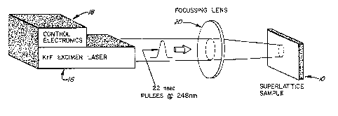
Figure 3 is a block diagram of an apparatus for
selective intermixing of a superlattice, constructed in
accordance with the principles of the present invention, and
utilizing an excimer laser as the energy source;
Figure 4 is a block diagram of an apparatus for
selective intermixing of a superlattice, constructed in
accordance with the principles of the present invention, and
utilizing a frequency-doubled Nd:YAG laser as the energy
source;
Figures 5 and 6 are, respectively, Raman
scattering profiles of an as~grown region of the sample in
Figure 1 and a region of the sample which has been
irradiated with a single pulse from a KrF excimer laser;
Figures 7 and 8 are, respectively, sputter-Auger
composition depth profiles of an as-grown region of the
sample in Figure 1 and a region of the sample which has been
irradiated with a single pulse from a KrF excimer laser; and
Figures 9 and 10 are Raman scattering profiles of
an as-grown region of the sample in Figure 2 and a region of
the sample which has been irradiated with five pulses from a
frequency~doubled Nd:YAG laser.
In the process of this invention multilayered semi-
conductor structures are selecti~ely intermixed by an
annealing treatment. Such structures may be superlattices,
or compositional superlattices. Such structures may consist
of as few as two layers, as, for example, a quantum-well
layer and a barrier layer. Similarly, such structures may
consist of either single or double heterostructures. More
generally, such layered structures comprise many layers, of
alternating quantum-well and barrier types, each layer of
the structure having a thickness ranging from about 5 to
about 500 A and thus constituting up to several hundred
atomic layers. Doping superlattices may also be employed
a~d, where specific effects may be desired, other types of
layers may be interspersed as well. The total thickness of
the layered semiconductor structure may be as great as from
about 5 to about 10 microns, thus ranging from about 50,000
to about 100,000 A.
In the process of this invention, the annealing
treatment may be conducted at any desired temperature,
selected primarily for convenience in operation. Generally
preferred temperatures include ambient temperature, while
permissible temperatures range down to 0C and lower or up
to several hundred degrees C although a generally acceptable
range extends from about 0C to about 50C. Pressure is not
a critical variable and operation at ambient pressure is
generally preferred.
In the process of this invention, a surface layer
of the multilayered semiconductor structure is irradiated
with an energy source which is adapted to provide an energy
density which is sufficient to effect the desired inter-
mixing between alternating layers. It has been found that
this can be readily accomplished, with surprising ease and
effectiveness, by employing a pulsed or a rapidly scanned
laser beam or electron beam as the energy source. Combina-
tion of such beams may also be employed. One preferred
energy source comprises pulsed excimer laser beams, parti-
7'7,~:~9
cularly the RrF laser beam, having a wavelength of 248
~anometer~,
Th~ energy density should be selected to avoid
signif icant damage to the multilayered struCture, Thedesired effect is an intermi~ing which provides selected
lateral and/or vertical regions which exhibit optical, opto-
electronic, and/or electronic properties which are different
from those of the original semiconductor structure. In some
instances this will comprise the conversion of a composi-
tional superlattice to an alloy structure. One proposed
mechanism for this result, by which we do not wish to be
bound and mention only for discussion purposes, would
involve a selective melting of portions of the structure,
followed by recrystallization, thus implying th~t very high
temperatures are achieved. If this be so, then it is
apparent that the existence of such high temperatures must
be limited to periods of short duration to avoid possible
physical damage to the structure.
In the practice of this invention, it has been
observed that in some instances a single pulse of a pulsed
laser beam is sufficient to accomplish the desired inter-
mixing. Often it has been observed that only a few pulses
are required. Similar energy densities are achieved by the
rapid scanning technique.
The degree of intermixing decreases gradually from
the surface of the multilayered sample to a depth depending
upon the energy density, after which the original composi-
tional modulation remains intact. However the intermixing
is believed to be a cumulative process.
In optimizing the process of this invention with
respect to the degree of intermixing, a heated sample mount
may be employed to minimize thermal gradients within the
semiconductsr structure and substantially reduce residual
lattice damage and strain.
From the foregoing description, it can be seen
that the present invention provides a novel and improved
process for selective intermixing of superlattice layers by
~2~7~
irradiating with a single pulse from a laser. Further, the
irra~iation can be with multiple laser pulses or other
combinations oE rapidly scanned laser and electron beam
sources, so as to increase the degree of intermixing. This
process should also be applicable to a wide range of other
layered structures including, but not limited to, metallic
superlattices and semiconductor superlattices in different
crystal systemsO
In the drawings, Figure 1 represents a multilayer
structure 10 composed of separate layers of thin solid
films, réferred to as a superlattice, comprised of 40
periods. Each period consists of a quantum-well layer 12
and a barrier layer 14. In the superlattice 10, each
quantum-well layer 12 has a thickness of approximately 100
and each barrier layer 14 has a thickness of approximately
100 A. The quantum-well layers 12 have a smaller band gap
and may be formed of a semiconductor material such as
gallium arsenide (GaAs). The barrier layers 14 have a
larger band gap and may be formed of a semiconductor
material such as aluminum gallium arsenide (AlxGal_xAs) with
aluminum mole fraction x=0.3. The value of x=0.3 has been
chosen as an illustrative example; other values can also be
easily used. Figure 2 shows another superlattice structure
lOa, having 40 periods, with each period consisting of a
GaAs quantum-well layer 12a and a Alo.3Gao.7 As barrier
layer 14a. Each of the quantum-well layers 12a has a
thickness of approximately 50 A, and each of the barrier
layers 14a has a thickness of approximately 100 A.
Figures 3 and 4 illustrate apparatus utilized for
selective intermixing of a superlattice in accordance with
the principles of the present invention. Each apparatus
includes an energy source or laser device 16 or 16a which
generates a pulsed output with a varying amount of energy
per pulse under the control of a power controller 18. The
laser device 16 is a commercially available krypton fluor~de
(KrF) excimer laser operating at a wavelength of approxi
mately 248 nanometers (nm) with a pulse duration of about 22
~7'74~9
nsec. The excimer laser is provided with a single-shot or
multiple-pulse firing capability. The laser 16a is a
commercially available frequency-doubled Q-switched/~d:YAG
(an acronym for neodymium; yttrium, aluminum and garnet3
laser having also a single-shot or multiple-pulse firing
capability. The Nd:Y~G laser operates at a wavelength of
approximately 532 nm with a pulse duration of about 10 nsec.
The output of the laser device 16 or 16a is directed onto
the superlattice sample 10 or lOa via a focussing lens 20.
The energy density incident on superlattice sample 10 or 10a
is varied ~y adjusting the laser pulse energy or the
focussed spot size at the sample surface.
Other available energy sources include a rapidly
scanned continuous wave (CW) laser or a pulsed or rapidly
scanned electron beam. The laser wavelength and incident
power are chosen with respect to the absorption length and
thermal diffusion properties of the layered structure so
that a sufficient power density is deposited in those
regions of the sample which are to be intermixed. The pulse
duration of the pulsed energy source or the local dwell time
(scan rate) of the rapidly scanned CW energy source are
chosen with respect to the stability of the various elements
or compounds in the layered structure so as to avoid
chemical decomposition of, or mechanical damage to, the
structure during the intermixing process. Such times have
been determined to be much less than a second for the
structures described in the following examples.
The following examples serve to illustrate,
without limitation, the process of this invention and the
novel, improved semiconductor products made thereby.
~xample I
A semiconductor superlattice structure sample was
3~ selected, consisting of 40 periods of gallium arsenide
quantum-well layers, having a thickness of 100 A, and
3~
alumin~m gallium arsenide (Alo 3Gao 7AS) barrier layers,
also having a thickness of 100 ~, as shown in Figure 1. The
salnple was irradiated in selected areas, employing the
apparatus of Figure 3 with a KrF laser at 248 nm wavelength,
with a ~eries of 22 ns pulses where the energy density was
va~ied from about 100 to about 900 mJ/cm2.
For energy densities exceeding about 400 mJ/cm~
(in a single 22 ns pulse), visible damage (cratering,
probably due to decomposition of the GaAs and Al~Gal_x~s
layers) was induced in the sample. For an incident energy
density of 220 mJ/cm2, no visible crystal damage resulted.
However, the reflective properties of the irradiated region
were altered, giving rise to a surface which, although not
lS cratered or roughened, appears slightly different even to
the naked eye.
Example II
A semiconductor superlattice structure sample was
selected, consisting of 40 periods of gallium arsenide
quantum-well layers, having a thickness of 50 A, and
aluminum gallium arsenide (Alo 3Gao 7As) barrier layers,
having a thickness of 100 ~, as shown in Figure 2. The
sample was irradiated in selected areas, employing the
apparatus of Figure 4, with a frequency-doubled Nd:Y~G laser
at 532 nm wavelength, with a series of 10 ns pulses where
the energy density was varied from about 50 to about 400
mJ/cm2.
When the laser intermixing was performed with a
single pulse of 10 ns duration and an estimated energy
density of 400 mJ/cm2 incident on the sample surface,
visible damage ("cratering") was induced. However, when an
energy density of approximately 50 mJ/cm2 was used there was
no visible crystal damage due to the irradiation by a single
pulse.
~2~7~3~
Example III
~ aman scattering spectra were measured on as-grown
and excirner laser-irradiated regions of the sample 10 of
Figure 1 (see Example I) for evaluation of the degree of
intermixing produce~ by the present invention. Figure 5
shows the Raman spectrum of an as-grown region of the sample.
~s can be seen, a longitudinal optical (LO) phonon pea~
appears at a fre~uency of 292 cm~l due to the pure Ga~s
layers and a Ga~s-like LO phonon peak appears at a frequency
of 281 cm~l due to the Alo 3Gao 7As layers. Figure 6
presents the Raman spectrum from a region of the same sample
which has been irradiated by a single excimer laser pulse at
an energy density of approximately 200 mJ/cm2. AS seen,
lS only a single GaAs-like phonon peak is observed, at a
frequency of 286 cm~l, corresponding to an intermixed
~lxGal_x~s alloy of the expected median composition where
x=0.15. These data indicate that extensive intermixing of
the original superlattice layers in the sample has occurred.
Example IV
The extent of the interdiffusion of the GaAs
layers and the Alo.3Gao 7As layers was determined by the
technique of sputter-Auger profiling, which utilizes a
combination of physical sputtering and Auger electron
spectroscopy to generate a composition-depth profile of the
layered structure. Figure 7 shows both Ga and ~1 depth
profiles through the first 21 periods (to a depth of about
4200 A) of the as-grown region of the sample 10 in Figure 1.
The effect of laser irradiation (see Example I) is dramatic
as shown in Figure 8. Complete intermixing of the first 11
periods (about 2200 ~) has occurred. In addition, the
transition from the intermixed phase to the unperturbed
superlattice structure is observed to be very abrupt. The
~1 mole fraction of the intermixed alloy is very close to
x=0.15, as expected. The above data indicate that the
excimer laser irradiation is capable of generating complete
13
7~
intermixing of GaAs/~lxGal_~As s~lperlattice layers, with
abrupt vertical transition between the intermixed and
unmixed regions.
~xample V
Raman scattering spectra were also measured on
as-grown and Nd:YAG laser-irradiated regions (see Example
II) of the superlattice sample lOa of Figure 2. Figure 9
Io shows the Raman spectrum of an as-grown region of the sample.
Again, LO phonQn peaks appear at frequencies of 278 cm~l and
290 cm~l, corresponding to the Alo 3Gao 7As and GaAs layers,
respectively. Figure lO shows the Raman spectrum from a
region of the same sample which has been irradiated with
five pulses from the ~d:Y~G laser 16a of Figure 3 at an
energy density of 120 mJ/cm2 for each pulse. The single
relatively narrow LO phonon peak at a frequency of 283 cm~
corresponds to a thoroughly intermixed AlxGal~xAs alloy of
median composition x=0.2, as expected from complete inter-
mixing of the original layered structure. In addition, aprominent symmetry-forbidden transverse optical (TO) phonon
peak is observed at a frequency of 266 cm~l, indicative of
microscopic lattice damage or strain. This may be due to
thermal gradients within the volume of the sample irradiated
by the Nd:YAG laser, since the output beam from this device
has been observed to provide a non-uniform intensity profile.
It is believed that microscopic lattice damage and strain
can be minimized by ensuring laser beam uniformity and, in
addition, by using a heated sample mount to reduce thermal
gradients in the sample during irradiation.
Example VI
A semiconductor superlattice structure sample was
selected, consisting of ~0 periods of gallium arsenide
layers, having a thickness of lO0 ~, and aluminum gallium
14
arsenide (Alo 3Gao 7~s~ layers, having a thickness of 100 A,
uniformly doped with silicon to a concentration level of
about 6xl017cm~3 The laser apparatus of Figure 4 (~xample
II) was employed for irradiation with a series of 10 ns
pulses where the energy density was varied from about 50 to
about 4~0 mJ/cm2.
At energy densities greater than about 70 mJ/cm2
visible damage at the surface was observed.
BEST MODE FOR CARRYING OUT T~E I~V~NTION
The best mode for operating the process of this
invention substantially follows the procedure set forth in
Example I. The selected layered semiconductor structure is
intermixed by irradiation with a pulsed excimer laser beam,
generally providing an energy density ranging from about 100
to about 400 mJ/cm2 at a dwell time of from about 10 to
about 30 ns. Both quantum-well and barrier layers may vary
in thickness preferably from about 3~ to about 150 A. There
are no specific requirements for temperature and pressure
parameters so that ambient conditions are generally to be
preferred.
While there has been illustrated and described
what is at present considered to be a preferred embodiment,
or best mode for conducting the present invention, it will
be understood by those skilled in the art that various
changes and modifications may be made, and equivalents may
be substituted for elements thereof, without departing from
the true scope of the invention. In addition, many modifi-
cations may be made to adapt a particular situation ormaterial to the teachings of the invention without departing
from the central scope thereof. Therefore, it is intended
that this invention not be limited to the particular embodi-
ment disclosed as the best mode contemplated for carrying
out the invention, but that the invention include all embodi-
ments falling within the scope of the appended claims.
INDUSTRIAL APPLICABILITY
The process of this invention is ideally suited to
provide a novel and direct tailoring of properties of semi-
conductor structures to provide novel materials for perfor-
mances not hitherto attainable. A simple, direct selective
intermixing for layered structures affords both lateral and
vertical modification of the doping, mobility, band gap, and
refractive index in electronic, optoelectronic, and optical
components, including field-effect transistors, lasers,
detectors, waveguides and bistable switching ele~ents.
By elimination of doping, it becomes possible to
provide such novel and improved components in a higher
degree of purity and reproducibility.