Note: Descriptions are shown in the official language in which they were submitted.
SPECIFICATION
TITLE OF THE INVENTION
Compound Semlconductor Device with Laminated Channel Layer
BACKGROUND OF THE; INVENTION
The present invention relates to a compound semicon-
ductor device, more partic~larly, to a compound semicon-
ductor device specially suited for manufacturing component10 device of integrated circuits (IC) and large-scale inte-
grated circuits (LSI) among those compound semiconductordevices such as field effect transistors (FET), high
electron movement transistors (HEMT) and the like.
As fabricating method of compound semiconductor de-
vic~s, particularly electronic devices, the epitaxial
growth method is generally employed owing to the thin anduniform growth of layer and ease of control of constituent
element composition ratio. Above all, the molecular beam
epitaxial ~MBE) growth method is known as one of the
particularly noticed techniques recently. For examplel a
device utilizing the MBE growth method and thin layer
periodic structure is described in details by W. T. Tsang
in Nikkei Electronics No. 308, 163 (1983).
According to this MBE growth method, the crystal
growth speed can be controlled on a single atomic plane
-- 2 --
~.2~4~
level (see J. P, van der Ziel et al., J. ~ppl. Phys., 48
(1977), p. 30183, and, furthermore, when combined with the
reflective electron diffraction method, the composition of
one atomic plane can be accurately controlled (see J. H.
S Neave et al., Appl. Phys. A 31, 1, 1983).
By employing such MBE growth method, it is possible
to fabricate a high electron mobility transis~or (HEMT) as
shown in Fig. 10.
~ Incidentally, microwave elements using conventional
compound semiconductors are disclosed, for example, in the
Japanese Unexamined Patent Publication Nos. 4085/1984 and
147169/1983.
BRIEF DESCRIPTION OF THE DRAWINGS
In the accompanying drawings:-
FIG. 1 i~ a simplified sectional diagram denoting a
preferred embodiment of FET as the compound semiconductor
device related to the invention
FIG. 2 is a chart denoting the result of evaluating
the dependency of the drifting speed of electron in the
FET shown in FIG. 1 on the intensity of the applied elec-
tric field;
FIG. 3 is a chart denoting the result of ev~luating
the dependency of the drifting speed of electron on the
intensity of the applied electric field when varying the
thickness of the well layer comprised of InAs against the
barrier layer comprised of InP;
FIG. 4 is a chart denoting the result of evaluating
the dependency of the drifting speed of electron on the
intensity of the applied electric field when varying th~
thi~kness of the well layer comp~ised of InAs against the
barrier layer comprised of GaAs;
FIG. 5 is a chart denoting the result of evaluating
the dependency of the drifting speed of electron on the
intensity of the applied electric field when varying the
thickness of the well layer comprised of InO 53Ga~ 47AS
against the barrier layer comprised of InP;
FIG. 6 is a chart denoting the result of evaluating-
the dep~ndency of the drifting speed of electron when
silicon is doped against the barrier layer comprised of
InP against the well layer comprised of InAs and also when
neither of these layers is doped with silicon;
FIG. 7 is a chart denoting the energy band consti-
tution of the compound semiconductor;
FIG. 8 ~s a chart of energy composition for ex-
plaining the quantized level;
FIG~ 9 is a chart explaining the phenomenon in
which highly energized electrons transit themsel~es from
the well layer to the barrier layer;
FIG. 10 is a simplified sectional diagram of a
conventional HEMT;
FIG. 11 is a chart denoting the result of
~ 4 ~ ~7744~
evaluating the dependency of the electron mobility on the
intensity of the applied electric field proper to a con-
ventional HEMT; and
FIG. 12 is a chart denoting the result of evaluat-
ing the dependency of the drifting speed of electron of a
variety of conventional compound semiconductors on the
intensity of the applied electric field.
In the HEMT structure shown in Fig. 10, a GaAs layer
12 functioning as a buffer layer is formed on a semi-
insulating GaAs substrate 11, and an undoped GaAs layer 13
serving as a channel layer is formed thereon. On the
undoped GaAs layer 13 is formed an electron supply layer
14 having a high impurity concentration such as
n-GaxAll xAs, and in the middle of the electron supply
layer 14 there is a layer 15 made of a semiconductor
containing p-type impurities at high concentration and
possessing a large electrophilic ability, while a gate
electrode 16 is disposed on this layer 15. Furthermore,
the surface region 17 of the electron supply layer 14 at
both sides of the layer 15 is alloyed, and source and
~27~ 0
drainage electrodes 18 are formed thereon.
In thus composed semiconductor device, when a proper
bias voltage is applied to the gate electrode 16, a two-
dimensional electron gas 19 is Eormed at the channel layer
13 side at the interface of the electron supply layer 14
and the channel layer 13. As a result, many electrons
flow in the portion Of a few tenS angstrom units in thick-
ness near the interface in the channel l~yer 13 where only
few impurity ions are present. Therefore, scatter of
impurity ions which is one of major causes of limiting the
electron mobility is less, so that a high electron
mobility may be realized.
However, when operating such a conventional compound
semiconductor device having the typical constitution men-
tioned above, the electron mobility is extremely dependent
on the intensity of the electric field applied to thetwo-dimensional electron gas. High electron mobility is
realized in low electric field application, conversely the
electron mobility lowers in high electric field applica-
tion. This phenomenon is described by M. Inoue e~ al. in
J.J.A.P.22 357 (1983) for example. FIG. 11 shows one of
thesa examples related to the constitution of the above-
menticned microwave element containing GaAs/n-GaxAIl xAs,
in which the above phenomenon is expressed by the broken
line curve.
~L277440
Generally, those phenomena including inter-valley
scattering, impact ionization, or phonon scattering re-
spectively cause electron scattering mechanism in a semi-
conductor device in high el~ctric field application.
Cons~quently, those characteristics specified below of thesemiconductor crystals used for channel layers of ultra-
high-frequency transistors should be improved.
( 1 ) To prevent inter-valley scattering from occur-
~ rence, a greater value of energy difference ~E should be
provided between valleys of space ~.
( 2 ) To prevent impact ionization from occurrence, a
greater value should be provided for energy gap Eg.
(3) ~o minimi~e loss of operating energy of carrier
electrons caused by phonon scattering, a lesser value
should be provided for effective mass m*.
FIG. 7 shows an example of the energy band structure
of GaAs crystals in conjunction with parameters of energydifference QE between valleys and energy gap Eg.
Conventionally, GaAs, InP, and InO 53Gao 47As respec-
tively make up compound semiconductors for composing chan-
nel layers of conventional FET and HEMT. Table 1 repre-
sents approximate values of energy difference ~E between
valleys, energy gap Eg, and the effective mass m* of
electrons of those compound semiconductors mentioned
above. With reference to the later description, data
related to InAs and InSb are also shown in Table 1. Note
that the energy difference between valleys of
0 53 0.47As is not yet known.
TABLE 1
~ Energy difference
Energy gap between valle s (eY) Effective
Elements Eg (eV) ~ r L -a E r x M a s s m *
GaAs 1.428 0.294 0.46 0.065
InP 1.351 0.5 0.85 Q.077
1 0 _ . _ _
InAs 0.356 0.78 1.47 0.027
C-O ~7A ~ 1 U ~1
As is clear from Table 1, if the channel layer is
composed of GaAs compound, since there is large energy gap
Eg, impact ionization rarely takes place in high electric
field application. Conversely, due to small energy
difference ~E between valleys, inter-valley scattering
easily takes place. Furthermore, since the effective mass
m* of electrons inherent to GaAs is great; a greater
amount of operating energy of electrons is lost by phonon
scattering, thus preventing electrons from flowing
themselves faster. On the other hand, if the channel
layer is composed of InP compound, due to substantial
~Z~744~
values of energy gap Eg, energy differences ~ErL, ~ErX
between valleys inherent to Inp, neither impact ionization
nor inter-valley scattering easily occurs in high electric
field application, thus allowing electrons to flow
themselves at a faster speed. Conversely, since the ef-
fective mass m* of electrons inherent to InP is great,
electrons are presented from flowing themselves at a
faster speed in low electric field application. On the
other hand, if the channel layer is composed of compound
semiconductors made from InAs or InSb, due to small amount
of effective mass m*, electrons flow themselves at an ex-
tremely fast speed in low electric field application.
Conversely, since the energy gap Eg is small, impact
ionization easily occurs in high electric field applica-
tion. For example, impact ionization occurs in the
compound semiconductor made of InAs in about 3.3 KV/cm
electric field application. Further, if the channel layer
is composed of compound semiconductors made of the mixed
crystals of InO 53Gao 47As~ this mixture exhibits a
2~ specific characteristic which is between those of compound
semiconductor made of InAs and compound semiconductor made
of GaAs. Those features thus far described above are
apparently identified by referring to FIG. 12 showing the
results of tests and theoretical development in conjunc-
tion with the dependency of the drift speed of electrons
- 9 ~
present in compound semiconductors on the intensity of
electric field applied thereto. Results of evaluating th~
characteristic of compound semiconductors made of GaAs are
cited by Ruch. J.G. and Kino G.S. in the Phys. Rev., 174,
921 ~1969), and by Houston P.A. et al. in Solid State
Comm., 20,197 (1977), respectively. Likewise, results of
evaluating the characteristic of compound semiconductors
made of InP are cited by Nelsen L.D. in the Phys. Lett.,
A38, 221 (1972) and Boers P.M. in the Electron Lett., 7,
625 (1971), respectively. Results of evaluating the
characteristic of compound semiconductors made of InAs are
cited by Itoh et al. in the report ED83-77, (1983) pre-
sented to Electronic Communication Society of Japan.
Covering the results of evaluating the characteristic of
compound semiconductors made of InSb, refer to the reports
presented by Glicksman M. et al. in the Phys. Rev., 129,
1572 (1963), Neukermans A. et al. in the Appl. Phys.
Lett., 17, 102 (1970), and Smith J. et al. in the Appl.
Phys. Lett., 37, 797 (1980), respectively. Results of
evaluating the characteristic of compound semiconductors
made of mixed crystals of InxGal xAs are cited by Itoh et
al. in the report ED83-77, (1983) presented to Electronic
Communication Society of Japan.
Generally, when operating either an FET or an HEMT,
since either of these is subjected to several kilovolts
-- 10 --
127~74~(~
per centimeter of electric field, any of these transistors
having a conventional structure using channel layers made
of InAs or InSb which easily allow occurrence of impact
ionization in low electric field incurs much disadvan-
tages. Actually, there is no satisfactory FET incorporat-
ing channel layers made of either InAs or InSb. In other
words, any of these conventional transistors cannot effec~
ti~ely apply advantageous characteristic of InAs or InSb
which allows electrons to flow themselves at an extremely
10 fast speed in low electric field application. Although
not shown in FIG. 12, those compound semiconductors made
of mixed crystals of InxGal xAs (0 < x < 1.0) or InAsyP1 y
(0 < y < 1.0) ~ary their dependency of the electron mobil-
ity on the intensity of electric field according to values
15 of x and y. However, the electron mobility of these com-
pound semiconductors is lower than that of those which are
made of InAs in low electric field application, and yet,
the electron mobility of these is also lower than that of
those which are made of either GaAs or InP in high elec-
20 tric field application, respecti~ely.
In order to securely manufacture high-performance
transistors featuring faster operating speed and more
satisfactory characteristics, those transis~ors should
allow electrons to flow themselves at an extremely fast
25 speed even in low electric field application. Taking this
~Z774AO
into ac~ount, neither GaAs having the low electron mobil-
ity in high ~lectric field application nor InP having the
low electron mobility in low electric field application is
i.deally suited for making up channel layers, respectively~
A study on a new constitu~ion called "super-lattice
con~titution" has been underway, the detail of which is
presented by L. Esaki, R. Tsu; I~M J. Res. Develop. (1970)
P 61 for example. As shown in FIG. 8, using an adequate
growth system like MB~ growth method for example, thin-
film layers made of compound semiconductors comprising
different components like Ga~s and AlAs for example are
alternately and periodically laminated. By comparative
evaluation of bulk crystals, specifically quantiæed levels
are then generated in the thin-film layers in the lower
portions of the conduction band (which are substantially
layers A shown in FIG. 8 and are hereinafter called "well
layers"). Although FIG. 8 shows only two levels 1 and 2,
actually, the number and the energy of the level are vari-
able dep~ndent on the thickness LW of the well layer,
thickness LB of the barrier layer corresponding to the
layer B shown in FIG. 8, and the difference between the
bottoms of the conduction band of layers A and B as the
bulk crystals, respectively.
Furthermore, the probability of the presence of elec-
trons in these quantized levels is described by M~ Jaros,
- 12 -
~27~
K.s. wong; J. Phys. c: Solid state Phys., 17 (1984) L765
for example. Assume that the barrier layer is made of
GaO 8Alo 2~s and the well layer is made of GaAs, respec-
tively, then, as shown in FIG. 9-a, only the quantized
leveis 1 and 2 can be confined inside of the GaAs layer,
whereas the high-energy level above levPl 3 exceeds the
barrier height EB of the barrier layer made of
GaO 8Alo 2AS. FIG. 9-b denotes that there is the greater
probability of the presence of electrons.on the side of
GaAs layer at levels 1 and 2 when the above condition is
present. Conversely, there is the greater probability of
the presence of electrons inside of the layer made of
GaO 8Alo 2As. The probability of the presence of elec-
trons is variable by varying the thickness of the barrier15 layer and the well layer and the height of barrier as
well. More particularly, as is clear from FIG. 9, there
is the significantly greater probability of the presence
of those electrons having more amount of energy than the
barrier energy in the GaO 8Alo 2As layer than those which
move through the GaAs layer. However, since the electron
mobility inside of the GaxAll xAs layer of the periodical
thin-film constitution made of mixed crys~al of GaAs and
GaxAll xAs is significantly low both in high and low
electric field application, when the high electric field
~5 is appli~d, the electron mobility inside of the GaxAll xAs
layer becomes lower than that of the GaAs layer measured
in the same intensity of electr:ic field.
Taking the above conditions into accou~t, the inven-
tor detected that specific energy band structure identical
to those which are shown in FIGS. 8 and 9 could be gen-
erated by making up the well layer by using either InAs or
InSb and the barrier layer by using either InP or GaAs.
First, when making up the well layer and the barrier layer
by using InAs and InP, respectively, the inventor detected
that the quantized level could be formed inside of the
InAs layer. The inventor also detected that only the
low-energy levels 1 and 2 could be confined in the InAs
layer, whereas the high-energy level 3 could be raised to
a point higher than the barrier height E~ between InP and
InAs as shown in FIG. 9. As a result, since the effective
energy gap Eg inside of the InAs layer is equal to the
difference ~etween the quantized level 1 inside of the
conduction ~and and the quantized level 1 inside of the
valence band shown in FIG. 8, this energy g~p becomes
greater than the essential energy gap Eg of the InAs
crystal. Consequently, as described earlier, impact
ionization cannot easily take place, thus allowing high
electric field of greater magnitude to be applied.
Alternativelyl in the presence of a specific intensity of
electric field prior to the occurrence of impact
~Z~7~
ionization, the probability of the presence of highly
energized electrons can significantly grow on the part of
the InP layer ~refer to the state of level 3 shown in FIG.
9) .
Consequently, it is possible for the InAs layer to
securely prevent impact ionization from internally taking
place. In addition, since those electrons transitted into
the InP layer in high electric field application follow
the electric characteristic of the InP layer in high elec-
tric field application, as shown in FIG. 12, electrons
flow themselves through the InP layer at a speed faster
than that of those electrons flowing through other cry-
stals even when high electric field is applied. In other
words ! in low electric field application, since electrons
are confined inside of the InAs layer, electrons flow
themselves at a speed faster than those electrons flowing
through the GaAs and InP bulk crystals, and yet, since`
highly-energized electrons transit themselves into the InP
layer in high electric field application, electrons are
allowed to flow themselves at a speed faster than those
which flow through the GaAs crystal.
SUMMARY OF THE INVENTION
This invention is contrived in the light of the above
problems, it is hence a primary object of this invention
-- 15 --
is to present a novel compound semiconductor device having
channel layer made of periodically laminated thin-film
constitution capable of moving electrons at an extremely
fast speed independent of the intensity of electric field~
Another object of the invention is to provide a novel
compound semiconductor device ha~ing channel layer made of
periodically laminated thin-film constitution which pre-
vents occurrence of intex-valley scattering and impact
ionization.
To achieve the above objects, the compound semicon-
ductor device related to this invention comprised channel
layer made of periodically laminated compound semicon-
ductor thin-films substantially being different from each
other. The energy difference between the conduction band
and the valence band of the compound semiconductor thin-
film layers of one side making up said channel layer is
less than that of the compound semiconductor thin-film~
layers of the other side, moreover the electron mobility
in low electric field application of one side compound
semiconductor thin-film layers is greater than that of the
other side, besides, the electron mobility in high elec-
tric field application is less than that of the other side
compound semiconductor thin-film layers, and/or the impact
ionlzation of the valence electron generated in high
electric field application takes place earlier than the
- 16 -
:~27~0
other side compound semiconductor thin-film layers. The
energy difference between the conduction band and the
valence band of the other side compound semiconductor
thin-film layers is less than that of the one side com-
pound semicondu~tor thin-film layers, and yet, the ~lec-
tron mobility in high electric field application is
greater than that of the other side thin-film layers.
When low electric field is applied, conduction electrons
preferentially flow through the one side compound semi-
conductor thin-film layers, whereas the highly-energized
conduction electrons by acceleration preferentially flow
through the other side compound semiconductor thin-film
layers. Furthermore, before causing conduction electrons
to generate impact ionization of valence electrons and
inter-valley scattering in the conduction band of conduc-
tion electrons in the compound semiconductor thin-film
layers of one side, conduction electrons which are highly
energized by acceleration generated by the applied high
electric field are allowed to smoothly transit themselves
from compound semiconductor thin-film layers of one side
to the other side compound semiconductor thin-film layers.
The compound semiconductor thin-film layers of one
side are of compound - --
~Z~7~4~
- 17 -
semlconductors m~de of InAs or InSb, whereas the compound
s~miconductor thin-film layers of the other side may be of
compound semiconductors made of InP or GaAs, respectively.
The canpound semiconductor thin-filtn layers of one side may ~e
of compound semuconductors made of either InAs or InSb, whereas
compound semiconductor thin-film layers of ~he oLher side may ~e of
colr~ound semiconductors made of mixed crystals of InAsyPl y(O
< y < 1.0). Alternatively, compound semiconductor thin-
film layers of one side may be of compound semiconductors
made of mixed crystals of InAsyP1 y (0.5 < y < 1.0),
whereas the other side compound semiconductor thin-film
layers may be of compound semiconductors made of mixed
crystals of InAsyP1 y (0 C y < 0.5), respectively.
Since the compound semiconductor device related to
this invention featuring the constitution mentioned above
is made up channel layers by periodically laminating
compound semiconductor thin-film layers of one side and
the other side compound semiconductor thin-film layers, it
is possible for the device to effectively generate energy
gap having a specific magnitude enough to prevent impact
- l8 - ~ ~7~
ionization from occurrence in the compound semiconductor
thin film layers of one side, and/or promote the probabil-
ity of the presence of highly energized electrons enough
to completely prevent lmpact ionization from occurrence in
the compound semiconductor thin-film layers of the other
side.
Furthermore, since the device related to this inven-
tion causes conduction electrons to be confined in the
compound semiconductor thin-film layers of one side in low
electric field application in order that the conduction
electrons can preferentially flow through the compound
semiconductor thin-film layers of one side, these conduc-
tion electrons are allowed to move themselves at a signif-
icantly accelerated speed. Likewise, since the device
related to this invention allows the highly energized
conduction electrons to preferentially flow through the
other side compound semiconductor thin-film layers after
being accelerated by the applied high electric field, the
mobility of these electrons can eventually and signifi-
cantly be accelerated.
In particular, before causing the conduction elec-
trons to generate impact ionization of valence electrons
and before occurrence of inter-valley scattering in the
conduction band by the conduction electrons, the device
related to this invention allows the highly energized
- I 9 - ~..;~L~
conduction electrons accelerated by the applied high elec-
tric field to transit themselves from the compound semi-
conductor thin-film layers of one side to the other side
compound semiconductive thin-film layers, and as a result,
the conduction electrons can preferentially flow through
the other side compound semiconductor thin-film layers at
a significantly accelerated speed.
DESCRIPTION OF THE PREFERRED EMBODIMENTS
Referring now more particularly to the accompanying
drawings, one of the preferred embodiments of this inven-
tion is described below by way of illustration and without limitation
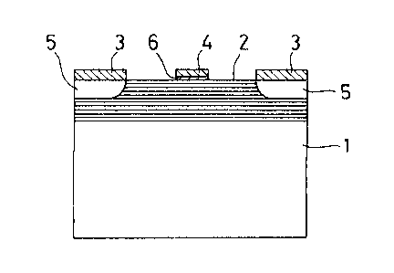
FIG~ 1 represents a novel FET related to this inven-
tion incorporating a channel layer comprised of a crystal-
line compound semiconductor multiple thin-film layer 2
containing each 6 layers of InAs and InP alternately being
laminated by about 69A and about lOOA on the semiinsulated
InP substrate 1. The multiple thin-film layer 2 has about
0.1 ~m thickness as a whole, which is formed on the semi-
insulated InP substrate 1 by applying the MBE growthmethod.
The surface of the multiple thin-film layer 2 is
provided with the evaporated AuGeNi ohmic junction elec-
trodes 3, to form the source electrode and drainage elec-
trode. Gate electrode is made of the Al Schsttky junction
- 20 ~
electrode provided on the insulated layer 6 hy evapora-
tion.
Due to the evaporation and alloying processes done
for gen~rating the AuGeNi ohmic ju~ction electr~de 3, the .
Au atoms diffuse itself throughout the crystalline multi-
ple thin-film layer 2 of compound semiconductor. As a
result, periodic characteristic of the layer structure in
the compound semiconductor crystalline multiple thin-film
layer 2 goes out of order, thus causing the crystalline
structure in the area 5 to eventually become identical to
the conventional InAsyPl y mixed crystal. Consequently,
the energy band structure in this area 5 also becomes
identical to that of the conventional InAsyP1 y mixed
crystal. Due to these phenomena took place during tests,
the inventor smoothly formed ohmic junction. N. Holonyak
et al. already announced similar phenomenon in which the
diffusion of the atoms causes the destruction of the peri-`
odic characteristic of the layer structure of compound
semiconductor multiple thin-film layers in A.P.L. 39
(1981) 102.
By applying conventional techniques for making up
conventional FET structures, the inventor confirmed that
the source electrode 3, drainage electrode 3, and the gate
electrode 4 shown in FIG. 1 properly ex~cuted functions
needed for FET.
- 21 - ~2~
FIG. 2 is the chart denoting the result of evaluating
the dependency of the drifting speed of electrons inside
of the multiple thin-film layer 2 shown in FIC. 1 on the
intensity of the applied electric field. As is clear from
the comparison to FIG. 12, while low electric field is
applied, the multiple thin-film layer 2 allows electrons
to flow themselves at a specific speed almost correspond-
ing to that is available inside of InAs. In addition, the
multiple thin-film layer 2 doesn't cause impact ionization
to occur even when high electric field is applied, while
allowing electrons to flow themselves at a specific speed
almost corresponding to that is available inside of InP.
In other words, by implementing the multiple thin-film
layer constitution shown in FIG. 1, the dependency of the
electron mobility on the intensity of electric field is
significantly improved. In addition, by varying the
thickness of the InAs thin-film layer from about 24A to~
about 75A, the inventor observed satisfactory effect cor-
responding to those which are mentioned above. Con-
cretely, the inventor confirmed the dependency of the
drifting speed of electrons on the applied electric field
by providing the thickness of the InAs layer at about 21A,
O O O O
24A, 45A, 75A, and 78A (refer to e, c, b, a, and d shown
in FIG. 3) against the thickness of the InP layer of about
lOOA. When the InAs layer had thickness at about 21A,
- 22 -
electrons flowed themselves at a low speed in low electric
field application. Conversely, when the InAs layer had
thickness at about 78A, the drifting speed of electrons
was increased until applied electric field rose to a cer-
tain level. When the applied electric field exceeded acertain critical level, the specimen was eventually des-
troyed. Taking this into account, the dependency of the
electron mobility on the applied electric field can se-
curely be improved by setting the thickness of the InAs10 layer at a certain value between about 24A and a maximum
of 75A. It was probable that, since the InAs layer had a
too large thickness, preferential flow of electrons inside
of the InP layer didn't occur even when high electric
field was applied, thus causing a large amount of current
to flow through only the InAs layer to eventually destroy
the specimen.
Although the above preferred embodiment employed the
well layer and the barrier layer respectively being com-
posed of InAs and InP, the inventor also achieved the20 identical effect by employing the well layer and the bar-
rier layer respectively being composed of InAs and GaAs.Use of these layers composed of the latter components
resulted in the lowered electron mobility in high electric
field application, which was slower than those which are
shown in FIGs. 2 and 3, while the elect~on mobility became
- 23 -
almost equal to that was observed from the GaAs bulk cry-
stal. This characteristic was observed only when the
thickness of the InAs layer was varied from about 24A to
about 6OA.
FIG. 4 is the chart denoting the result of evaluating
the dependency of the drifting speed of electrons on the
applied electric field when employing the well layer and
the barrier layer respectively being composed of InAs and
GaAs. The inventor confirmed the results shown in FIG. 4
by evaluating the dependency of the drifting speed of
electrons on the applied electric field by providing the
O O O
thickness oE the InAs layer at about 21A, 24A, 60A, and
72A (refer to c, b, a, and d) against the thickness of the
GaAs layer at about 50A. Concretely, when the InAs layer
has the thickness at about 21A under low electric field,
electrons flow themselves at a low speed in low electric
field application, and therefore, the InAs layer should be
provided with a minimum thickness at about 24A.
According to the test results, when the InAs layer
had the thickness at about 72A, a variety of defects took
place with the specimen due to unsatisfactory surface
condition of the tested specimen. However, the specimen
generated mirror surface when the InAs layer had the
thickness at about 21A, 24A, and 60A, respectively.
Taking this into account, the dependPncy of the electron
~.Z77~40
- 2~ -
mobility on the applied electric field can securely he
improved ~y providing the thiclcness of the InAs layer at
from about 24A to about 6 OA.
Of the multiple thin-film layer 2 of the ~'ET shown in
FIG. 1, when using well layers which are respectively
comprised of InO 53Gao 47As and provided with the thick-
ness at minimum of about 68A against the barrier layer
comprised of InP, the inventor confirmed that the electron
mobility in high electric field application was almost
equal to that was shown in the InP.
FIG. 5 is the chart denoting the result of evaluating
the dependency of the drifting speed of electrons on the
applied electric field when employing the well layer and
the barrier layer respectively being comprised of
InO 53Gao 47As and InP- Concretely, the inventor con-
firmed the dependency of the drifting speed of electrons
on the applied electric field by providing the thickness
O O O O
InO 53Gao 47As layer at about 65A, 68A, lOOA, and 200A
(refer to d, c, b, and a shown in FIG. 4) against the
thickness of InP layer at about lOOA. When the layer
comprised of InO 53GaO 47As had the thickness at about
65A, the drifting speed of electrons slowed down in low
electric field application, and thus, the InO 53Gao 47As
layer should be provided with a minimum thickness at about
68A.
7~
- 25 -
When using the well layer comprised of InSb against
the barrier layer comprised of GaAs or InP, the inventor
confirmed that satisfactory result identical to that of
FIG. 2 was obtained. When low electric field was applied,
electrons flow th~mselves at a speed almost equal to the
electron mobility inside of the InSb. Likewise, when high
electric field was applied, electrons flowed themselves at
a speed almost equal to the electron mobility inside of
GaAs or InP. It was also confirmed from these experiments
that impact ionization was completely prevented from oc-
currence inside of the InSb layer.
The invention also provides other constitutions, in
which the well layer may be comprised of either InAs or
InSb and the barrier layer may also be comprised of
InAsyP1 y (0 < y < l.0). In addition, the well layer may
also be comprised of InAsyP1 y (0.5 < y < 1.0) and the
barrier layer may also be comprised of InAsyP1 y (0 ~ y
0.5)-
As a result of doping n-type impurities such as sili-
con (Si), tin (Sn), tellurium (Te), and the like against
only the barrier layer portions of all those combinations
mentioned above, the inventor successfully promoted the
electron mobility by 20% through a maximum of 50% in low
electric field application.
FIG. 6 is the chart denoting the results of
.
- 26 -
evaluating the dependency of the drifting speed of elec-
trons on the intensity of the applied electric field when
using the well layer comprised of InAs crystal having the
thickness at about 75A and the barrier layer of InP cry-
stal having the thickness at about lOOA. Reference char-
acter "a" in FIG. 6 indicates the result of the doping of
silicon against only InP layer portion, whereas reference
character "b" indicates the result without doping silicon
against both InAs and InP layers. By referring to these
results, the inventor eventually confirmed the effect
described above.
As is clear from the foregoing description of the
preferred embodiments of this invention, the thickness of
the entire channel layer can be set in the submicron
order. Accordingly, by effectively applying those con-
stituents of the preferred embodiments to a variety ofcompound semiconductor devices for making up IC and LSI,
it is possible for all the electronic elements to securely
accelerate their operation speed independent of variable
conditions of the applied electric field.
Although the foregoing description of the preferred
embodiments totally refers to the use of FET, it is ob-
vious for those skilled in the art that the constituents
of the invention can securely generate the same charac-
teristics as the above by effectively being applied to
.: .
- 27 -
other compound semiconductor devices like HEMT and others.