Note: Descriptions are shown in the official language in which they were submitted.
~ ~777~
A Median Filter
This invention relates to a median filter which is a device
which receives an input signal representing a sequence of input
values and produces an output signal representing a series of
output values each of which is the median of an associated group
of input values.
The invention arose when considering the design of a median
filter for processing video signals in which each of the
aforementioned input values represents the intensity of an
associated pixel and in which these values appear at a very high
rate. The design of a median filter for this purpose, using
known techniques is relatively complex leading to the need for
substantial capital investment in the initial design work and in
preparations for manufacture e.g. using integrated circuit
techniques.
This invention provides a median filter comprising a number
of identical modules each arranged simultaneously to receive the
current value of an incoming digital signal, each module
comprising a feedback shift register which can be set to receive
its input at any one of its stages, means for setting the shift
registers of the different modules to receive their inputs at
different stages, means associated with each shift register for
comparing the contents of one stage with the content
r~
.
~ 27~7~;~
of each other stage to de~ermine whether the content of
that said one s~age is the median value, and means for
passing it to an output in response to such a detection.
Each of the aforementioned ~modules" can be
relatively simple compared with a conventional median
filter and can accordingly be accommodated on a single
integrated circuit of a sufficiently small size to be
economical to design and to tool up for manufacture.
Furthermore, the number of input values in each "group"
from which the median is selected is determined only by
the number of modules. Thus, different filters having
different characteristics can be made in accordance with
the invention simply by including different numbers of
modules in them. Alternatively a standard filter having a
large number of modules (possibly included in a single
integrated circuit) can be adapted to be set so as to make
use of just some of the modules as required. It would be
possible to make a provision to change the number of
modules used and therefore the characteristics of the
filter automatically in response, for example, to the
amount of background noise detected in the input signal.
The means for setting the feedback shift register can
conveniently be provided by a number of selectors, one
associated with each stage of the shift register, for
optionally feeding to that stage the content of a previous
s~age or the input signal, and means for setting the
selectors so that the input signal is passed ~o a chosen
~.~77~
one of the stages and so that each of the other staqes
receives the output from the previous stage.
One way in which the invention may be performed will
now be described by way of example with reference to the
accompanying drawings in which:-
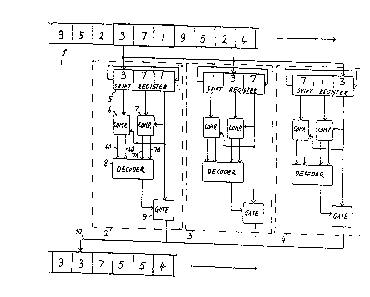
Fig. 1 is a schematic block diagram of a median
filter constructed in accordance with the invention, and
Fig. 2 is a more detailed diagram of one of the shif t
regis~ers indicated generally by the reference numeral 5
on Fig. 1
The illustrated filter is for fil~ering a video
signal in digital form to remove high frequency components
characteristic of background detail.
Referring firstly to Fig. 1 the series of numbers
shown at 1 represents 10 successive examples of the
incoming signal 4259173253 in that order. These are
applied to the inputs of three modules 2,3 and 4. In the
module 2 the input signal is applied to the first cell of
a three stage feedback shift register 5 so that, after
enterinq any three successive numbers, such as the
numbers 1,7,3, the first number appears in the third
stage, the second number appears in the second stage and
the third number appears in the first stage.
The outputs of the first and second stages are
applied to logic circuits 6 and 7. Circuit 6 compares the
contents of the first and third stages of the shift
register and produces a logic signal 1 on lin~ 6A if the
~Z7773~3
- 4 --
lat~er is grea~cr ~han the former, and the logic signal 1
on line 68 if they are the same. The circuit 7 compares
t~e contents of the second and third stages and produces a
logic signal 1 on line 7A if the latter is greater than
S thc former and a logic signal 1 on line 7B if they are the
same. The outputs 6A,6~,7A,7B form a code having 16
possible values, three of which are indicative of the
content of the third s~age being the median. The decoder
8 responds to the presence of any one of these codes by
enabling the gate 9 to pass the content of the third stage
to the filter output 10.
The module 3 is identical to the module 2 except thàt
the input signal is applied to the second stage of the
shift register of module 3. Consequently the first number
of the sequence shown at 1 appears in the first stage, the
second number of the sequence appears in the third stage
and the third number of the sequence appears in the second
stage.
The module 4 is also identical to the moduLe 2 except
that the input signal is applied to the third stage of the
shift register. Consequently the first number of the
sequence is applied to the second stage, the second number
of the sequence is applied to the first stage and the
third number of the sequence is applied to the third
stage.
From the foregoing it will be apparent that the
first, second and third numbers of the sequence are
~2777~3
applied to thc ga~cs 9 of the thrcc modulcs but only ~hat
which represents the median is passed to the output 10.
The shift registers are of a special design which
enables them to be identical but to be set so as to except
S their inputs at different stages. The shift register S of
module 2 will now be described with reference to figure 2.
The input to shif~ register 5 is applied to the
inputs labelled ~A~ of 3 selectors 5A,SB and SC. These
are controlled by binary control signals on lines SD,SE
and SF generated by a one of three decoder SG. The latter
is programmed externally by fixing the potentials on its
two inputs 5H and SI. In the case of decoder SG its two
inputs are set at values 0. This produces codes on lines
SD,SE and SF such as to select input ~A~ of SA and input
lS ~B~ of S~ and SC.
The inputs corresponding to SH and SI of the shift
registers in module 3 are set such as to cause the
equivalent of SB to select input ~A~ and the equivalent of
SA and 5C to select input ~B~.
The inputs corresponding to SH and SI of the shift
registers in module 4 are set such as to cause the
equivalent of SC to select input ~A~ and the equivalent of
SA and SB to select input "B".
The components SA,SB,SC and SG thus constitute means
for setting the shift register to receive its input at a
particular chosen stage.
It will be appreciated that the illustratcd filtcr is
127771~
dcsigncd to calcula~e the median of groups of 3 input
values. A group of 3 has been selected for simplicity of
dcscription and it will be appreciated that larger groups
containing any odd number M of input values could be
processed in an analogous fashion providinq the shift
registers have a similar number M of stages and provided
there are a similar number M of modules available for use.
Where the shift registers have a larger number of stages
than is required for a particular filtering purpose each
selector 5A,SB and SC can be constructed and controlled so
as to feed to its associated shift register stage either
the input signal or a chosen output from any of the other
stages; or no signal at all. In this way the effective
size of the shift registers can be controlled as can the
number of modules operative at a given time.
Further features of the invention will appear from
the accompanying appendix entitled ~Algorithms and
Implementations for Median Filters".