Note: Descriptions are shown in the official language in which they were submitted.
777S5
OPTICALLY BlSTABLE DEVICE
The invention relates to an optically bistable device, and more particularly to
such a device in the form of a Fabry-Perot etalon.
05
Optical bistability in Fabry-Perot etalons is known, and there are two known
techniques for achieving it. The first approach is described in a standard
textbook, "Optical Bistability: Controlling Light With Lightn, H M Gibbs,
Academic Press, New York, 1985. ln essence, this approach employs an optically
nonlinear material in a Fabry-Perot etalon cavity. The etalon is illuminated with
a comparatively low power light beam at a wavelength near an etalon
transmission maximum or interference fringe. As the power light beam is
increased, by virtue of optical nonlinearity the cavity material refractive index
changes and with it the optical path length in the cavity. This chan~es the
position of thç ctalon transmission maximum with respect to wavelength. The
light beam wavelength then lies closer to the centre of an etalon interference
fringe, and etalon transmission switches from a low to a high value. This may
be rcfcrrcd to as "all optical'l bistability, in which a change In thc input optical
power induccs switching. Khoo, Normandin and So describe an example of this
in J Appl. Phys. S3(11), Novcmbcr 1982. They cmployed a liquid crystal layer
S0 ~m thick retaincd bctween two microscope slidcs, this cell being arranged
bctween the mirrors of a Fabry-Perot etalon. The etalon mirror separation was
variable, and optical bistability as a function of input optical power was
demonstrated for four mirror separation ~alues. In Optics Leffers, Vol. 8, No.
2S I, January 1983, Cheung, Durbin and Shen demonstrated optical bistability as a
function of input optical power in the presence of a magnetic field. They
employed a Fabry-Perot ctalon having an 83 ~m cavity width filled with liquid
crystal material. Multiple bistable loops were observed as the input optical power
was varied between 0 and 40 Watt cm~2 with IBI = 1.3 kOe.
The second approach to obtaining optical bistability involvcs the use of clectrical
feedback (as opposed to optical feedback). This is described by Stewart, Bennionand Goodwin, Phil. Trans. R. Soc. Lond. A313 (1984) 401. In this technique, a
Fabry-Perot etalon is employed containing an intracavity electro-optic medium.
An electric field is applied to the medium. Light transmitted by the etalon
~,. . .
lZ77~SS
produces an electrical signal at a detector, and the signal is fed back to control
the magnitude of the electric field in the medium. The refractive index of the
intracavity medium varies in response to the electric f~eld. Positive feedback is
arranged to occur; ic an increase in input op~ical power is arranged to change
05 the electric field sucb that an etalon cavity transmission maximum or interference
fringe occurs closer to the input optical wavelength.
The disadvantage of either of the foregoing prior an approaches is that they
require a change in the input optical power to induce optical bistability. This
10 may be a consequence of internal optical feedback in a nonlinear intracavity
material, or alternatively it may be a consequence of electrical feedback via anexternal circuit. However, for many electro-optic signal processing applications it
is required to employ a constant input optical power level. This is because it is
frequently inconvenient to vary optical power, which requires for example
15 cumbersome nonideal optical modulators.
It is an object of the present invention to provide an optically bistable devicewhich does not rcquirc a change in input optical power to induce optical
bistability,
The preunt in1vcntion provides an optically bistable device including a
Fabry-Perot etalon containing intracavity optically nonlinear material and arranged
to exhibit optical bistability, and wherein:
(1 ) the cavity material refractive index is electro-optically tunable via
etalon biassing means to move an ctalon interference fringe maximum from
a wavelength Aml to a wavelength ~m2~
(2) a light source having a wavelength ~s is arranged to pass light through
the etalon, where ~m2 lies between ~ml and ~5, ~s and the source intensity
being arranged to initiate optical bistability at an etalon fringe wavelength of~m2 but to be inappropriate for bistability at a fringe wavelcngth Of ~m1
and
-2-
'~
127775~
-- 3 --
(3) the etalon biassing means are connected to a variable voltage source
arranged at least for etalon fringe maximum tuning from ~`ml t ~m2.
The invention provides two major advantages over prior art devices. Firstly, it is
05 capable of construction in simple form at low cost; in one embodiment the cavity
material is a layer of liquid crystal material, and the cost is very small as istypical of liquid crystal devices generally. Secondly, the invention prDvides
optical bistability induced by change in applied bias voltage. It is not necessary
to change the input optical intensity or provide an external electrical feedback10 loop as in the prior art. The invention accordingly provides fast switching by
virtue of the positive feedback or regenerative action associated with optical
bistability, but without the prior art intensity modulation or electrical feedback
complications. It is the electro-optic equivalent of a Schmiet trigger circuit.
15 The etalon cavity material preferably has an optical nonlinear refraction
parameter n2 at least equal to 10~ cm21Watt to allow operation at input powers
in the milliwatt region or below. In addition, the material preferably has an
electro-optic coefficient and thickness appropriate for cavity phase tuning through
at Ieast a bistable Joop in response to a bias voltage change of 10 Volts. The
20 cavity material may be a liquid cry~tal materlal having a birefringence of at least
0.05, and preferably In the range 0.09 to 0.11.
The etalon may hcorporate mirrors which are optically partially absorbing to
produce the temperature rise stimulus required for optical bistability.
25 Alternatively, the cavity material itself may be absorbing, such as a liquid crystal
material containing a dye component having an appropriately located optical
absorption band. The invention may alternatively be a Fabry-Perot etalon in
which the cavity is a multiple quantum well structure exhibiting optical
nonlinearity and dectro-optic tunability.
In an alternative aspect, the invention provides a method of obtaining optical
bistability including the steps of:
12'777S~
-- 4 --
(I ) providing a Fabry-Perot etalon arranged for optical bistability and
containing intracavity optically nonlinear material, the cavity material
refractive index being electro-optically tunable via etalon biassing means to
move an etalon interference fringe from a wavelength ~mt to a wavelength
05 )`m2~
(2) illuminating the etalon with light having a wavelength )`s~ where )`m2
lies between ~ml and ~5~ )~s and the light intensity being arranged to
initiate bistability at an etalon fringe wavelength Of ~m2 but to be
inappropriate for bistability at a fringe wavelength of 1~ml~ and
(3) altering etalon bias to produce etalon fringe maximum tuning from ~ml
to 1~m2-
In order that the invention might be more fully understood, embodiments thereof
will now be described with reference to the accompanying drawings, in which:
Figure 1 is a sectional view of an electro-optic device of the invention;
Pigure 2 h a graph of optical transmission against optical path Icngth (OPL) or
cavity phasc for thc Pigure 1 dcvice;
Pigure 3 is a graph illustrating optical bistability in an idealised Fabry-Perot ctalon;
Pigure 4 is a graph of the oscillatory Airy transmission function of a
Fabry-Perot etalon against cavity intensity, and is crossed by stra;ght
lines of constant incident intensity;
Figure S illustrates the function of Figurc 4 plottcd against incident intensity to
show typical optical hysteresis or bistable loops;
Figure 6 shows the Airy function of Figure 4 plotted aga;nst cavity intensity and
crossed by lines of constant cavity phase shift due to applied clectric
fleld;
Figures 7 and 8 are graphs of output intensity versus electric field applied to the
cavity for positive and negative va1ues of dn/d ~, which give rise to
anticlockwise and clockwise bistable loops respcctively;
Figurcs 9 and 10 are cquivalent to Figurcs 6 and 7 at increased input intensity;Figure 11 is a graph similar to Figure 10 and illustrates the effect on bistability
-4-
12m55
of changing the initial cavity phase;
Figure 12 is a graph of Fabry-Perot etalon transmission against wavelength
illustrating fringe shift due to electro-optic and bistable effects;
0S Figure 13 is a sectional view of an alternative embodiment of the inventionincorporating zinc selenide cavity material and dielectric multilayer
mirrors; and
Figures 14 to 16 schematically illustrate embodiments of the invention based on
multiple quantum well structures.
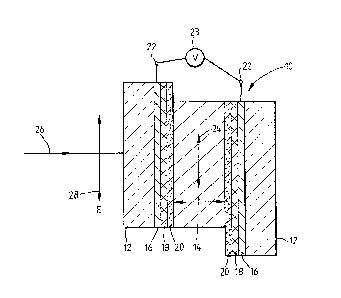
Referring to Figure 1, there is shown a sectional view of an optically bistable
electro-optic Fabry-Perot etalon 10 forming part of an optically bistable device of
the invention. The etalon 10 comprises two glass plates 12 acting as cell walls
for a liquid crystal material (LCM) layer 14 contained therebetween. The glass
lS plates 12 have respective internal wall coating layers of indiwn tin oxide (ITO)
16, evaporated silver 18 20 nm in thickness and evaporated silicon oxide 20
(SiO). These iayers are successively disposed so that the structure is
glassllTO/AglSiO/liquid crystal, le 12/16/18/20/14 from thc Icft of the ctalon 10
or thc reversc o- this ortcr from thc right. Thc ITO laycrs 16 arc electrodes
having dectrical bias connections 22 conncctcd to a variable voltage source 23.
The liquid cry,stal rnaterial of layer 14 is rcfcrred to as 3ISI7 PCH, and consists
of a three component mixture of rnatcrials each of the
,, cyano-phenyl-cyclohexane-alkyl variety. The components differ only in that their
alkyl chain lengths vary. Their structure i5:
. ~
nH2n ~ 1 { ~CN
' ' 30
', where the components have rcspecti~e values of n of 3, S and 7. The mixture
'~, proportions are 30% n = 3, 40% n = S and 30% n = 7.
;~ ~ The LCM layer 14 is 10 microns thick. Morc generally, a layer thickness in the
' 35 range S to 20 microns may be emp!oyed. The ~TO layers 16 are transparent
5_
;~
"~:
1~777~5
electrodes of known kind for establishing a voltage across the LCM layer 14.
The silver layers 18 are partially transmissive as required for a Fabry-Perot
etalon. In this example they are 70% reflecting, although a reflectivity of 30%
or more is adequate. A preferred range of reflectivity is 80% to 90%. The
05 SiO layers 20 are agents for aligning the long axes of the liquid crystal molecules
of layer 14 in the plane of the drawing parallel to the surfaces of the glass
plates 12 and layers 16 to 20, as indicated by an arrow 24. This alignment is
alterable by applying a bias voltage across the electrodes 16. Other alignment
agents such as rubbed polyamide may also be used, as is well known in the field
of liquid crystal devices. A light beam 26 is incident on the etalon 10
perpendicular to the layers 14 to 20. The light beam has an electric vector 28
parallel to the liquid crysta} molecule orientation 24.
The liquid crystal material of layer 14 has a large optical nonlinearity, ie therefractive index n is strongly dependent on the light intensity in the material. In
the nonlinear optics field, this nonlinearity is expressed by the parameter n2,
which should preferably be at least 1 o-6 cm2/Watt for the purposc of the
invention, The material of layer 14 should preferably also bave an electro-opticcoefficient which is sumci¢ntly large to pcrrnit tuning of the optical phase change
bctwecn mlrror layen 1~ through an cxcursion of at Icast lr/2 tA/4) in response
to a change iD bias of 10 Volts, and preferably through ~r to 2,r For a
thickness of layer 14 of 10 microns ttypical), 10 Volts corresponds to an electric
field of 104 Volts/cm Layer 14 may be composed of materials other than liquid
crystals provided that sumciently large optical nonlinearity and electro-optic
cocfficients are cxhibited However, the foregoing propcrties required of layer 14
may be collectively expresscd in the case of liquid crystal materials by statingthat the material birefringence should be at least 0.05, a typical range being 0.05
to 0.15 and preferably 0.09 to 0.11. A further criterion is that the liquid crystal
absorption coefficient cY should preferably be less than 2000 cm~l to maintain
sufficient etalon finesse
The mode of operation of the etalon 10 will now be described in outline, a
more detailed analysis being given latcr. As has been said, the liquid crystal
molecules are aligned in the absence of bias in the direction of arrow 24 parallel
to the electric vector 28 of the illuminating light beam 26, and the beam 26
--6--
~75~
experiences a liquid crystal refractive index of 1.61. Application of a bias
voltage across electrodes 16 rotates the molecular orientation to~vards the electric
field direction, ie the direction of beam 26 and the perpendicular to layers 14 to
20. As is well known in the liquid crystal device fietd, the bias is AC, the
05 molecules responding to the RMS value. A sufficiently large electric field ~vill
reorientate the liquid crystal molecules to substantial parallelism to the electric
field direction. The 1iquid crystal refractive index presented to the light beam 26
then becomes 1.49. The change in refractive index ~n occurring in the liquid
crysta1 material 3/517 PCH preferred to above is 0.12 for a change in molecular
orientation from paralle1 to perpendicular to the etalon layers 14 to 20. For a
liquid crystal layer thickness of 10 microns and at a light beam wavelength of
S00 nm, this birefringence value of 0.12 produces a Fabry-Perot fringe shift of
about 4 complete fringes when the bias applied across electrodes 16 changes by
S Volts RMS. The etalon 10 may accordingly be tuned in phase across, towards
lS or away from an interference fringe at a specific optical wavelength by adjusting
the bias voltage.
Refcrring now also to Pigure 2, thcre is shown a typical graph 30 of
Pabry-Perot ctalon transmi~ion against optical path 1cngth (OPL) or phase ~
20 (arbitrary units). The graph 30 has two transmission maxima or interference
fringes 32 and 34, A maximum in transmission occurs when the phase
being givcn by:
2 nt ( I )
2S where n = refractive index of material within etalon,
t = thickness of material within etalon (cavity length), and
)~ = wavelength of light transmitted by etalon.
- In the present invention the phase ~ is tuned electrically by varying the bias
30 ~roltage to change the refractive index n in Equation (1).
Referring now also to Figure 3, there is shown a graph 40 of Input Power versus
` Output Po ver (arbitrary units) for an idealised FaSry-Pcrot ctalon cxhibiting
optical bistability. The etalon contains a cavity material having a high X3 value,
--7--
. .
~27775~
-- 8 --
this being a coefficient indicating degree of optical nonlinearity. As the graph 40
shows, the output power or light intensity increases linearly with input power
from zero at the origin 0 to a f~rst point of bistability A. The refractive index
n of the eavity material is a funetion of temperature. The cavity material
D5 temperature increases by virtue of the optical power in the etalon, sufficiently so
that the etalon phase ~ reaches a value c}ose to that appropriate for an
interference fringe maximum. Positive feedback or regenerative action then takesplace. The increase jD transmission which occurs on approach to an interference
fringe produces a further change in refractive index. This shifts the phase ~
10 closer to the fringe maximum increasing transmission and changing the refractive
index once more, and so on. The effect is that the output power or transmined
intensity switches very rapidly from A to B in Figure 3 by virtue of the positive
feedback associated with optical bistability.
lS As the input power is reduced, the ouptut power reduces as indicated by the line
BC. When the point C i8 reached, the optica1 bistability effect occurs once
more but in the reverse direetion from high to low transmission or output power.The amount of input optical power required to reaeh the first switehing point A
is dependent on the eavity phase b of Equation (I ), whieh in turn depends on
20 input wavelength, eavity materia1 refracti-Je index at low power and eavity
thiekness t. If the eavity phase ~ at a particu1ar wavelength is re1ative1y far
from that appropriate for a fringe maximum, a relativdy large input optical
power level is required to produce switehing. If however ~ is elose to a fringe
maximum, on1y a eomparatively small input power level will affeet switching.
Referring once more to Pigure 1, in the present invention the etalon phase
ean be tuned to approaeh a fringe maximum simply by biassing the electrodes 16
appropriately. Switching between optically bistable states may then be initiated at
a constant input power or light intensity level under bias ~oltage eontrol. As is
30 well kno~vn in eleetro-opties, it is considerably simpler and faster to change a
bias ~o1tage than to alter a light intensity. To alter light intensity in a laser for
example, one requires a eumbersome variable optieal attenuator in the input laser
beam or means for ehanging the laser output power, both of whieh are slow to
operate. The present invention aeeordingly provides an electro-optic bistableS switeh of elegantly simple construction which i!i switchable faster than an
--8--
.
~27775~
g
other vise equivalent device lacking positive optical feedback. It may be employed
for c~ample to impose a digital code modulation upon a laser beam for
tetecommunications purposes. ln this application, the invention provides the
advantage that digital pulse rising and falliDg edges are of short duration alloving
05 high bit transmission rates. By virtue of its bistability the invention may also
provide a rcstorable optical memory for the electrical input. Other applicationsof the iDvention include tunable optica} filters, optical modulators and spatial light
modulators (light valves).
10 As has been said, in the foregoing embodiment optical bistability occurs in
rcsponse to etalon intracavity material temperature rise The temperature rise
mechanism in the etalon 10 of Figure I arises from optical absorption in the
si1ver etalon mirrors 18 Absorption in the 1iquid crystal layer 14 is insignificant.
Dielectric multilayer mirrors may aJternatively be employed. Since dielectric
IS mirrors do not absorb appreciably, the liquid crystal hyer 14 should be rendered
dightly absorbing by admixture of a dye component of known kind having an
appropriatcly locatcd absorption band,
In any dcvicc of the invention such as ctalon 10, there is a minimum light
20 intensity below which switching will not occur regardless of applied e}ectric field
This minimum will depend on etalon mirror reflectivitics and mirror or cavity
material absorption, and arises because podtive feedback requircs a degsee of
input powcr to initiate. S vitching may howcvcr bc obtaincd at bias voltages in
the region of 10 Volts when cavity materials, optical wavelengths and device
25 structures are chosen appropriately In other respects the wavelength in
particular is unconstrained provided that a cavity material is available having
appropriate propcrtics at that wavelength Materials such as liquid crystals and
wide band gap Il-Vl semiconductors wch as ZnS and ZnSe provide a large
spcctral range
The operation of the etalon 10 will now be analysed in more detail
The Fabry-Perot eguations relating transmission, T, and reflection, R, to the
front and back mirror reflectivities, RF and RB respectively, the cavity layer
35 absorption cocfficient, ~x and the thickncss t arc,
_g_
~27'775~
-- 10 --
T -- A 2 (2)
1 + F sin ô
B + F sin2~
05 R ~ ~ (3)
where
F -- 4R~/(I-R~)
~O
A - e ~Yt ( 1 -RF) ( 1 -RB)/( I _Ra) 2
B -- RF ~ 1 - (R~/RF) ] 2/ ( 1 -R~) 2
Rcy - (RFRB) ~ e txt
and ~ = 2~nttA = ctalon cavity phasc
20 whcrc n and t arc thc cavity material rcfractive index and thickness and ~ is the
1ight beam wavelcngth in frcc ~pace.
The cavity fincsse is Fc = ~rF~/2.
2S For the purpose of this analysis, it is assumed that:
. ~
(i) absorption in the LCM layer 14 is linear, and
(ii) refractive index change ~n is proportional to average cavity intensity,
c within the etalon.
Consider first only the optical nonlinearity or change ~n in thc cavity material
refractive index, and given by
~n - n2 I c
. ~ ,
-10-
,
,~ .
~ .
.~
,~:
SS
where n2 (the nonlinear refraction) is a constant by virtue of (ii) above, and
~ ~ ~o + ~op
05 ie
~o + ~lc
where ~0 and ~Op are rcspectively the initial cavity phase and the phase change
10 induced by cavity intensity change, and ~y is the change in ~Op per unit cavity
intensity change.
The phenomenon of optical bistability in an etalon of the invention will now be
described with reference to Figures 4 to 11, these comprising graphs in which
1 S ordinate and abscissa va1ues are expressed as dimensionless quantities to simplify
analysis.
An example of the oscillatory Airy transmisslon function T of cquation (2~ is
shown for a low cavity fine~se case in Pigurc 4 for RF = RB = 70% and
20 o~t - 1. Thc function is plotted against dimensionless cavity intensity ~ylJ~r. For
the purpose of this analysis, it is assumed that the rate of change of intracavity
material refractive index with cavity intensity, ie WdIC, is positive. The
transmission T at low cavity intensities is determined by the initial phase, ~0.The input-output characteristics of the nonlinear etalon are sensitive to thc value
2S of this initial phase value. ln Figure 4 ~0 = 0.
The relationship between cavity intensity lc and incident, reflected and transmitted
intensity, Il, R and T respectively, leads to the additional criteria:
T CT
_ I (6)
~ C
and
3S
~' ' -11 -
.
~s~
-- 12 --
(1-R) _ (7)
C
where CT and CR are given by
~5
o~t e ~t ( 1 -RB)
~1 - e ~ ~1 + RBe o~t~ (8)
[ ] [~ .' ]
Equations (1 ) and (6) are solved simultaneously to eliminate IC and describc the
1S nonlinear Fabry-Perot transmission as a function of incident intensity (~ in
cquation (1 ) is a function of Ic). This is shown in Figure 5. Equation (6)
describes straight lincs through the origin as shown in Plgure 4; the slopes of
theu lincs rcprcsent tifferent values of incident intendty, thc shallower dopcs
corrcsponding to higher intcnslties, BistabilJty occurs at multiple crossings of the
20 periodic snd traight lincs. Thus on increasing thc dimensionless incident
intcnsity ~llt1r from 3 to 4 in Pigure S, the transmission switches from A to B;on dccreasing the intensity again, the switch down is from C to D rcsulting in
input-output hystercsis.
25 Applying a bias voltage to the Fabry-Perot etalon 10 causes an additiona1 change
in the refractive index. For a fixed light intensity and a variab]e bias voltageproducing an electric field E across the etalon, a total phase change takes place
given by:
o + ~op + ~eQ (10)
ie
~o + 'YlC + ~E (11)
-12-
~: :
,, '
127775~
-- 13 --
where ~ is an electro-optic constant representing the electric field dependence of
the cavity phase and ~eQ is the change in cavity phase due to electric field.
The condition for an incident intensity, ~ = 2~r is shown again for the
05 foregoing example iD Figure 6 for a series of values of ~eQl~r from 0 to I.
This example assumes positive values of dn/d ~ . A multiple crossing occurs at
about ~eQ = 0.25 1r. Thus for a fixed incident intensity, increasing the electric
field will cause the cavity to switch from point A to B on the way up to C to
D on the way down. Figure 7 is equivalent to Figure 6 replotted as a function
I O of phase shift due to the electric fie}d E in units of ~r. lt shows bistability of
the optical output with an anti-clockwise loop with variation in electric field. If
dn/d ~ is of opposite sign to dn/dlc, then the characteristic of Figure 8 is
obtained with a clockwise loop.
I S The optical output does not necessarily return to its original value when the
etalon cavity bias voltage is turned off. Figures 9 and 10 are equivalent to
Figures 6 and 7, but now the input intensity is increased to yll = 3~r. With an
initial phase ~O = 0, as tbe voltage is increased the transmission will switch from
A to B, but thc rcvcrse swltch vill not occur on reducing the voltagc sgain to
0. The bistable loop in voltage can bc rctrlc~red by altering thc initial phase (eg
by etalon rotation), as illustrated in Pigurc Il for ~O = -0.6 s. The loop is
cnlarged for this higher input power case as compared to the lower power case
of Pigure 7.
Tbe advantages of having electrical and nonlinear optical control over a
Fabry-Perot etalon are as follows:
(a) Ability to tune the initial phase of the cavity electro-optically gives finecontrol over the characteristics of nonlinear optical bistable devices.
(b) The occurrence of bistability ~vith voltage offers a binary optical output
with ~roltage at constant optical input or a binary clectrically addressable
spatial light modulator.
(c) Optica1 nonlincarity gives fast sweeping of an clectrically tunable filter
into or out of the high transmission state becausc of regcncrative s vitching
; ~ .
- ~ 35 action.
',
--1 3--
1;~7775~
(d) Under the correct initial bias conditions, a nonlinear optical bistable
device can be reset by zeroing the voltage, thus av~iding the necessity of
interrupting the hold light beam as necessary in prior art devices.
(c) Additional clectro-optic feedback may be applied from output or input
05 optical signals to give further switching characteristics.
(f) Reflectivity and transmission are complementary in a Fabry-Perot
etalon, if one is high the other is low. Voltage control of this therefore
provides electrical selection of one of two light paths to route an optical
signal.
Referring now to Figure 12, there is shown a schematic graph of transmission
against wavelength for the etalon or optical modulator 10 of Figure 1. The
graph illustrates the mode of operation of the invention in terms of the
wavelengths of Fabry-Perot ctalon transmission maxima. A solid curve 60
lS itlustrates two. adjacent transmission maxima 62 and 64, which correspond to
incident light intensity much lower than that required for optical bistability and
zero voltage bias across clectrodes 22
Thc transmission maximum or interference fringe 64 occurs at a wavclength 1~ml
The ctalon 10 1~ illuminated by a light ~ourcc (beam 26 in Figure I ) having a
wavelcngth ~k WheD an appropriate bias voltage Vg is applied across etalon
bias conncctions 22, the ctalon transmission ma~imum 64 is shiftcd to 66 (chain
curvc) at a centre wavdength Am2. This ~hift occurs by virtue of
clectro-optically induced change in cavity material refractive index. The light
source 26 is arranged to have sufficient intensity to initiate optical bistability for
a fringe maximum at 1~m2~ but insufficient intensity to initiate this for a fringe
maximum at )~ml When the fringe maximum reaches l~m2~ optical nonlinearity
of the cavity materia1 produces a further shift in refractive index. For n2 c 0,- in accordance with Figure t2, the fringe centre wavelength is further reduced.
The fringe consequently shifts to 68 (dotted line) with ccntre wavclength ~m3~
which is just beyond ~5 relative to ~ml and l~m2- This is a ~nown phenomcnon
in optical bistability; the fringe maximum passes through the source wavelength so
that the latter becomes located just off the fringe ccntre.
:
.~ ..
~277~7S~
The foregoing analysis demonstrates that the criteria for electro-optically induced
optical bistability in accordance with the invention may be expressed as follows:
~1 ) the Fabry-Perot etalon contains optically nonlinear material having an
OS electro-optically tunable refractive index, and includes means such as
electrodc layers on the ctalon mirrors for electrically biassing the cavity
materia1;
(2) at a first etalon bias voltage (eg zero), the etalon has an interference
fringe centre at a wavclength ~ml . and this centre is tunable to Am2 by
changing the bias voltage;
(3) a light source illuminates the etalon, the source having appropriate
wavelength and sufficient intensity to initiate bistable switching at )`m2 but
insufficient intensity for this to occur at )`ml It does not matter whether
~s C )~m2 C l~m1 as in Pigure 12, or whether ~s > ~m2 > )`ml~ but in
the latter.case it is neccssary that n2 >
Thesc criteria are cnough to producc bistable switching under voltage control.
However, as prcviously indicated with refcrcnce to Piguru 4 to 11, thcy arc not
neccssarily sumcicnt to provide for switching in thc rcverse direction when the
bias voltage ~s rcset to its inlthl valuc. In this connection, Figure 10
dcmonstrates that thc initial optical state is not necessarily retrieved. Moreover,
the criteria do not necessarily provide for tuning through a complete bistable
IOOp. n may also be convenient, as has been said previous}y, to tune the etalon
phase through ~r, which is equ;valent to applying suMcien1 etalon bias voltage to
shift the centre of fringe 64 in Figure 12 to the wavelength of fringc 62. This
allows voltage tunability through a whole cycle of etalon cavity phase.
The switching conditions for optical bistability are determined by such parameters
as the size of the optical nonlinearity and cavity finesse. The design criteria are
~; 30 ~vell }no vn. They are described by H M Gibbs in the standard textbook
previously referrcd to, and also by:
.;
(a) D A B Miller, lEEE J. Quant. Elec., QE-17, 306 (1981), and
(b) B S Wherrett et al, J. Opt. Soc. Am. B, _, 351 (1986).
3S
-lS-
:`
,
~ 27775.~
-- 16 --
The invention requires that the Fabry-Perot etalon and illuminating light sourcebe initially in states not producing bistability, but the etalon cavity is tunab}e
electro-optically into bistability. If the initial etalon and source states are far
from bistability conditions, thcn a high degree of elcctro-optic tuning is
05 necessary. This in turn requires either a cavity material with a large
electro-optic coefficient, or a high electric field in the cavity, or both. Fromthe prior art of optical bistability, it is a straightfonvard design exercise to set up
an etalon and light source near bistability. Moreover, the change in cavity phase
to be produced clectro-optically to initiate bistability may then be calculated as
10 described earlier.
The electro-optic coefficient ~ may be defined as the refractive index change ~nproduced by a change in electric ~leld ~E, ie
. ~ _ ~n/~E (12)
~ is rclated to ~, defined in ¢quations 110) and (11) as the ¢lectric field
dcpcndence of cavity phase, by
~ _ 2 t ~ (13)
where t = cavity thickness and ~ = ~vavelength.
Etalon cavity phase ~ is given by
li 2 nt ( ~ 4 )
where n = refractive index.
30 Consequently, the change ~ in cavity phase produced by a change ~n in
refractive index is given by:
2~nt (
3S
--16--
1 277755
-- 17
lt may be required to tune the ehlon through some fraction f of a complete
interference fringe spacing, ie a phase change of f~r where 0 ~ f ~ 1.
Therefore
OS ~ f 2~nt ( 16 )
Combining equations (12) and (16):
~0 ~ ~ (17)
Since change in ehlon bias volhge ~V = t~
~ _ ~ (18)
tS f rnay be designed to produce a cavity phase change greater than the width of a
bishble loop by selection of a cavity material with sufficiently large ~ for anydcsircd bias voltage change ~V. The width of the bishble loop of course
dcpends on thc cavity material aDd etalon finesse, and i8 a matter of design
from optical bistability prior art,
Por f s 1, corrcsponding to ctalon tuning through a cavity phasc cycle:
~ _ ~ (19)
25 If it is required that ~V bc less than 10 Volts, thcn at an optical wa~clength of
micron ~ must bc grcater than S % I o-6 cm Volt~~, which is satisfied by
liquid crystals. However, lower values of ~ may be employed with higher values
of ~V and/or lower values of f, the fraction of a cavity phase cycle through
which there is electro-optic tuning.
Referring DOW to Figure 13, h which parts cquivalent to thosc pre~iously
described arc lilcc-refcrcnced with thc prcfix ~00, thcrc is uhematically shown a
furthcr embodiment 110 of the invcntion. The cmbodimcnt 110 is a Fabry-Pcrot
etalon comprising a 4.3 micron thicL~ cavity layer 114 of ZnSc sandwiched
35 between successively disposed layers of lTO clectrodes 116 and dielectric
17-
~,
;
~27775~i
-- 18 --
multilayer mirrors 118 this structure being supported by a glass plate 112. Eachmirror 118 consists of four quarter-wavelength dielectric layers two zinc selenide
layers arranged alternatively with ~wo thalium fluoride layers. This arrangement provides mirror reflectivities of RF ~ 0.78 and RB ~ 0.72 at 514 nm . The
OS cavity laycr 114 was grown by molecular beam epitaxy at pressures in the range
2 - 8 x 10~ mbar growth rates 0.6-0.9 micronslhour and substrate
temperatures of 30-40 C. The molecular beam was generated from a Knudsen
cell source containing ultra-high purity ZnSe prepared by chemical vapour
deposition from zinc vapour and hydrogen selenide. This arrangement exhibits
switching or optica1 bistability at 8 mWatts of 520 nm wavelength light under
zero bias voltage.
Referring now to Figures 14 IS and 16 which are not to scale there are shown
schematically illustrated embodiments of the invention incorporating multiple
IS quantum wclt- (MQW) structures. In Figure 14 an etalon 130 h shown
comprising an MQW structure 132 between partially reflecting metal mirrors 134
with respective elcctrical bias connections 136. The MQW structure 132 h 3 ~m
thick and comprises 100 GaAs laycrs each 10 nm thlck arrangcd alternately with
100 AlGaAs laycrs cach 20 nm thick. Three GaAs layers 138 and two AlGaAs
20 laycrs 140 src shown (not to scale) the presence of others being indicated bychain tines such as 142 Incident and transmitted light are indicated by arrows
144 ant 146.
Figure lS shows an ctalon lS0 comprising an MQW structure 152 bctween
25 dielectric mirrors IS4 consisting of quarter-wave taycrs. The MQW structure IS2
consists of layers such as 156 and 1S8 and is equivatent in chemical species andnumber of tayers ~o structure 132 of ctalon 130. However the structure 152 has
non-uniform doping to provide PIN diode characteristics. It consists of a p-type- region 152a an intrinsic or i region 152b and an n-type region 152c these
30 regions being illustrated as delimited by dotted lines such as 160 Electric bias
conncctions 162 are provided to the p and n type regions IS2a and 1S2c.
Incident and transmitted light are indicated by arrows 164 and 166. In operationthe PIN diode is reverse biascd.
-18-
127775,~
-- 19 --
Figure 16 shows a further etalon 170 comprising quarter-wave dielectric stacks
172a and 172b providing etalon mirrors. The mirrors 172a and 172b contain
therebetween an MQW structure 174 equivalent to structures 132 and 152 and
composed of AlAs hyers arranged alternately with AlGaAs hyers. The MQW
OS s~ructure 174 is of intrinsic or i eonductivity; the mirrors 172a and 172b are
p-type and n-type respectively to produce a PlN diode structure, and have
electrical bias connections 176a and 176b. Incident and transmitted light are
indicated by arrows 178 and 180.
The eta1Ons 130, 150 and 170 of Figures 14 to 16 operate in an equivalent
manner. GaAs-AlGaAs MQW structures exhibit a nonlinear refraction for photon
energies elose to the semiconductor bandgap energy. The nonlinearity is of
electronic origin, as opposed to the thermal equivalent of the Figure 1
embodiment, ~nd occurs on a faster timescale. In other respects the etalons 130,1S lS0 and 170 operate in a similar manner to that of F;gure 1. A bias voltage
applied across the electrical connections 136 of the etalon 130 produces an
electric fiekl in ~e MQW structure 132, which produces an assoeiated ~hift In
the absorptlon edge and the re(ractive index by virtue of the quantum con~med
Stark effect. In addition, optical bistability occurs due both to optical filling of
contuction bands with electrons and to saturation of excitonic absorption. The
etalon 130 is accordingly tunable by appl;ed voltage to induce optical bistability in
accordance ~vith the invention. Similar effects can be obtained in bulk
semiconduetors by virtue of the Franz Keldysh effect.
The etalons 150 and 170 operate in a similar manner to etalon 130. A bias
voltage applied across ~he electrieal connections 162 or 176a/176b produces an
electric field appearing predominantly in the l region 152b or 174. This
produces a refractive index change and voltage-tunable bistability as before.
Further details on the ebaracteristics of MQW structures may be obtained from
the following references:
(a) Gibbs et al, Appl. Phys. Lett. 41(3) pp221-2 (August 1983).
(b) 'Miller et al, Appl. Phys. Lett. 45(1) ppl3-lS (July 1984).
- 35 (e) Gourley, Superlattieu and Microstruetures 1(3) pp~27-30 (1985).
--19--
,