Note: Descriptions are shown in the official language in which they were submitted.
~2m73
-1- 20365-2784
BACKGROUND OF THE INVENTION
ield of the Invention
The invention relates in general to a method and appar-
atus for testing conductor networks by secondary emission and
which uses a large area second electron beam so as to prevent
false indications due to discharges.
Description of the Prior Art
Methods are known for testing electrical components, for
example, the publication by M. Brunner entitled "A Dynamic Single
E-Beam Short/Open Testing Technique", Scanning Electron Micro-
scopy/1985/III, Pages 991-999 discusses an electron beam which
has a primary energy that is held constant during the measurement
for charging conductor networks and for reading the potentials
occurring at the contact points according to the network geometry
so as to detect existing shorts o~ opens.
United States Patent 4,417,203 also discloses a method
and apparatus for non-contact testing of wiring modules for shorts
and opens using a plurality of electron beams.
The known methods, however, can only be operated without
error when the charge applied by the electron beam remains stored
in the network during the entire measuring procedure. Since not
all printed circuit boards and wiring modules have adequately high
insulation resistances of more than 1012 ohms, parts of the net-
work can be discharged by tracking currents to a degree wherein a
secondary electron signal measured in those regions indicates an
open which is not in fact present.
~7,~
~J~
~m73
-2- 20365-2784
SUMMARY OF THE INVENTION
It is an object of the present invention to provide a
method and apparatus for testing circuits wherein such discharge
is compensated so that inaccurate readings will not occur. In
particular, it is assured that the potential generated by a charg-
ing beam is stabilized at a higher level wherein the charge con-
dition of a first point of the line network is changed with a
first particle beam PE and either the first or a second particle
beam PE is directed onto a second point of the conductor network
and the charge condition of the second point is read by detecting
the secondary particles triggered at this point wherein at least
the points of the line network which are charged with the first or
second particle beam are also charged with a third particle beam
HS which has a particle energ~ EIIs ~o a~ to compen~ate ~or charge
losses occurring in the line network.
The advantage obtainable with the invention particularly
comprises that the printed circuit boards and wiring modules having
low insulation resistances can be checked for shorts and opens
without error.
Other objects, features and advantages of the invention
will become apparent from the following description of certain
preferred embodiments thereof taken in conjunction with the accom-
panying drawings although variations and modifications may be
effected without departing from the spirit and scope of the novel
concepts of the disclosure, and in which:
~27m3
_3_ 20365-2784
BRIEF DESCRIPTION OF THE DRAWINGS
Figure 1 is a plot of the energy relationship versus the
secondary emitted electrons; and
Figure 2 is a schematic view illustrating a printed
circuit board having a plurality of networks.
DESCRIPTION OF THE PREFERRED EMBODIMENTS
With a suitable selection of the energy of an electron
beam which is directed onto the surface of a non-conductive speci-
men, it can be achieved that the current of the primary particles
incident on the specimen is not compensated by the current of the
backscattered and secondary particles emanating from the surface.
It is critical for the charging event that the mean number of back-
scattered and secondary electrons triggered per incident primary
electron which is usually referred to as the yield of emitted
electrons which in thi~ speci~ication will be re~erred ~o as the
electron yield. ~he interdependence is schematically illustrated
in Figure 1. The electron yield passes through a minimum and then
usually reaches a maximum and then slowly drops again at higher
energy levels. In general, there are two energy values at which
20 ~ ( El ) = a (E2) = 1 which are shown as El and E2 in Figure 1. An
electron beam accelerated to those energies does not change the
charge condition of the specimen since an incident primary elec-
tron respectively triggers precisely one electron on the average.
The point El or, respectively, E2 are therefore also referred to
as the neutral point energies and typically El lies in the energy
range below 0.5 keV and point E2 with few exceptions lies in the
- 1277773
_4_ 20365-2784
energy range between 0.5 and 4 keV. When the specimen is irradi-
ated with electrons having an energy that does not coincide with
one of the neutral point energies El or, respectively, E2 then
the non-conductive parts of the specimen are gradually charged
positively (El ~ EpE ~ E2, a~ 1) or negatively (EpE ~ E~, EpE ~ El,
~ 1) until a state of equilibrium is established. ~or primary
electrons having the energy EpE > E2 this state of equilibrium is
achieved when the primary electrons are decelerated to such a
degree in the electrical field built up above the specimen such
that their incident energy just coincides with the neutral point
energy E2 characteristic of the respective surface material.
Electrons having the energy El ~ EpE < E2, however, are capable of
positively charging the specimen to only a few volts since the
kinetic energy of the emitted secondary electrons is too low to
leave the specimen any longer. So a5 to yenerate high positi~e
potential, the Recondary electrons must be extracted from the
specimen using an electrode.
By choosing a suitable energy of the charging beam thus
potentials of any operational sign can be generated on a specimen
particularly a conductor network. Since the energy distribution of
the emitted secondary electrons is influenced by existing specimen
potentials that charge condition or, respectively, the potential
at the trigger point of the secondary electrons can also be
qualitatively as well as quantitatively identified using an
electron beam positioned at the measuring point of interest. The
measured quantity is thus the respective secondary electron
~277773
_5_ 20365-278
current registered in a detector mounted above the specimen.
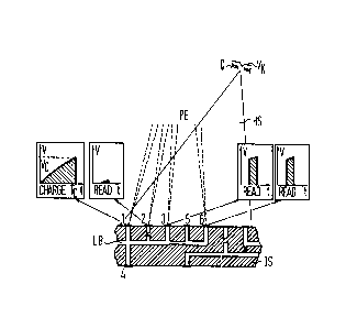
Figure 2 shows a portion of a plurality of networks of
a printed circuit board. The contact points 1, 2, 3 and 4 which
are arranged on the surface of an insulating layer IS with inter-
connects LB connecting these points defines a network A corres-
ponding to a desired electrical function. The contact points 5
and 6 together with the interconnects LB define a second network B
which is insulated from network A. The analogous case also applies
to the other contact points in Figure 2 which are not referenced
in detail. It can be assumed without limitation that the printed
circuit board is no charged before the beginning of the measurement.
So as to check the printed circuit board for shorts and
opens, one contact point, for example, contact point 1 of the net-
work A is first charged to a potential Vc using an electron beam
PE generated in the electron optic~l column o~ ~ modified scanniny
electron microscope and contact point 1 i5 charged with a time
constant TC depending on the capacitance of the network. The time
dependency of the contact point potential Vc is shown in the upper
left of Figure 2 in the form of a diagram with a leader connected
to point 1. When the desired charging potential Vc has been
reached, the electron beam PE is removed from point 1 and is
positioned to another contact point of the network A with unmodi-
~ fied primary energy so as to read the potential by recording the
;~ secondary electrons which are triggered at that point. When the
same secondary electron current, in other wordsr the same potential
VC exists at the charging point 1 within the measuring time then
1277773
-6- 20365-2784
the two points are connected to one another in a conductive
manner. This condition is met for contact point 3 as is shown in
the diagram at the upper right of Figure 2. On the other hand,
the contact point 2 remains uncharged because of an open which
occurs between contact points 1 and 2 so that a lower secondary
electron current is registered at point 2 in the detector. As
shown in the right-hand diagram of Figure 2, the same potential
occurs at charging point 1 also exists when the measurement is made
at scanning contact point 6. Thus, the two contact points 1 and 6
are thus necessarily connected to each other in a conductive
fashion which in this particular circuit means that there is an
undesired short between the networks A and B.
In order to reliably record shorts and opens by measur-
ing the potential present at the individual contact points, the
charges introduced in the netwo~k~ ~ and B must remain stored
during th~ entire measuring time. So as to compensate, for example,
the loss of charges resulting from the tracking currents in the
present invention, it is proposed that at least thos parts of the
printed circuit board which are to be scanned are scanned with
the electron beam PE are charged during the measurement with a
holding beam HS that covers these regions. For example, the hold-
ing beam HS can be generated using an electron source Q as shown
in Figure 2 which comprises a cathode, a Wehnelt electrode and an
anode that are expediently mounted laterally above the printed
circuit board which is to be checked in the specimen chamber of
the scanning electron microscope that generates the charging and/or
1277773
-7- 20365-2784
reading beam PE. The energy of the electrons of the holding beam
HS can be set by varying the anode potential such that the charge
losses caused in the conductor networks by tracking currents are
compensated. Since the energy EpE of the charging or, respectively,
the reading beam determines the energy EHS of the holding beam
e:Lectrons as described in the above publication by Brunner, the
charging and reading beam are identical. Different beams for
generating and reading the potentials are used in the method dis-
closed in United States Patent 4,417,203. Two different operating
modes which are referenced a) and b) are to be distinguished.
Operating mode a) EpE > E2 or EpE< El, EHS ~
the condition EpE - E2 ~ EHS - El must be met in case EpE > E2
and the condition El - EpE > EHS - El must be met in the case
EPE ~ El.
The holding beam HS which has the energy E~S ~ El (~or
example, EHS - El = 50 eV) stabilizes both the insulator IS as
well as the contact points 1 through 6 of the networks A and B to
a positive potential defined by the extraction field built up
above the printed circuit board with, for example, the assistance
of an electrode of the secondary electron detector, or to ground
in case the secondary electrons are not extracted. Since a
charging beam PE having an energy EpE > E2 or, respectively,
; ~ EPE < El negatively charges the contact point 1 of the network A
and all points 3 through 6 that are in conductive connection
therewith to the potential Vc (e Vc = EPE ~ E2 for EpE ~ E2 or,
respectively, eVc = EpE < El), the electrons of the holding beam
,
i~77773
-8- 20365-2784
HS are decelerated to an extent at these points such that they
reach these points with a final energy EHS - eVc < El. The yield
of emitted electrons thus becomes smaller than l and the contact
points are negatively charged to the potential VK of the cathode
oE the holding beam source Q (VK approximately = to -lO0 through
-ISOV), and the holding current automatically compensates any
charge losses caused by tracking currents. For surface-wide dis-
charge of the printed circuit board, the energy EHS of the holding
beam electron is briefly increased to a degree such that the
electron yield ~ is also greater than l at negatively charged
contact points
Operating Mode b) El ~ EpE ~ E2' HS
The holding beam HS which has the energy EHS ~ El (for
example, El - EHS = 50 eV) stabilizes both the insulator IS as well
as the contact points 1 through 6 of the networks ~ and B to the
potential VK of the cathode of the holding beam source Q i.e., for
example, to -100 through -150 volts. Since the charging beam PE
which has an energy El < EpE ~ E2 charges the contact point 1 and
all contact points 3 through 6 conductively connected thereto to a
positive potential defined by the extraction field built up above
the printed circuit board, the electrons of the holding beam HS
are accelerated in the region of these points, so that they reach
these points with a final energy of EHS + eVC (Vc indicates the
potential generated by the charging beam). The extraction field
must thereby be dimensioned such that the condition EHS + eVC~ E
is met. The electron yield thus becomes greater than 1 and the
1277773
_9- 20365-2784
contact points remain positively charged, and the holding current
automatically compensates for any charge loss. For large-area dis-
charge of the printed circuit board, the energy EHS of the holding
beam electrons is briefly reduced to an extent until the electron
yield also becomes smaller than 1 at the positively charged con-
tact points.
The invention is not limited to the exemplary embodi-
ments described. Thus, the invention is employable for all me~thods
for testing conductor networks, printed circuit boards, wiring
modules, hybrid circuits, SMD assemblies, and etc. wherein a
charge introduced into the network must remain stored during the
measuring time.
The invention is also directed to preserving the
uncharged condition by compensation of the capacitative charging
effects as well as for the change~ in pot~ntial caused by scattered
electrons.
It is also not necessary to irradiate the investigated
specimen simultaneously over the entire surface, but the holding
beam HS can also sweep its surface line-like.
Although the invention has been described with respect
to preferred embodiments, it is not to be so limited as changes
and modifications can be made which are within the full intended
scope of the invention as defined by the appended claims.