Note: Descriptions are shown in the official language in which they were submitted.
-- 1 --
The present invention relates to apparatus for microwave
telecommunications systems and more particularly to an
integrated microwave oscillator.
One of the usual requirements to be met by oscillators
is frequency stability regardless of temperature or other
circuit parameter changes, such as supply voltage vari-
ation. Usually the most important p~rturbation is caused
by A junction transistor or of an FET. Such variations
cause a considerable variation of the electrical para-
1~ meters (~ or ~), which cannot be directly compensated andhence a stabilizing element external to the device is
necessary. One widely used method uses a high stability
resonator with high quality factor (Q) placed at a suit-
able point in the circuit.
Stabilization takes place as follows. Oscillation fre-
quency is, as known, determlned by the existence of zero
reactance conditions in the circuit under working condi-
tions, and near the resonance frequency of the resonator
reactance variations of the active device due to tempera-
ture variations are compensated for by reactance varia-
tions of a high Q element caused by small shifts in fre-
quency. Such a resonator exhibits rapid change in reac-
tance in the vicinity of the resonance frequency, allow-
ing zero reactance conditions to be regained.
The resonant high Q element is frequently a dielectric
resonator. An exemplary application of such an element
is shown in United States Patent No. 4,149,127, in which
a dielectric resonator stabilized FET micro strip oscil-
lator is described, the resonator baing placed in the
gate connection. Feedback for starting oscillation is
obtained by a line o~ suitable length connected to the
source and terminated b~ a short circuit. This circuit
can supply a highly stable oscillation frequency, but
~ ~7~ 5~
-- 2 --
appears insufficiently prote~ted against the danger of
parasitic oscillations particularly at low frequencies,
since the impedance viewed from the source is a pure
reactance. To ovèrcome this problem, a resistive compo-
nent is needed which becomes effective only outside theoperating fre~uency band, thus reducing the overall cir-
cuit gain and hence the degree of positive feedback.
A recent embodiment of microwave oscillator, described in
a paper entitled "Efficient Low-Noise Three Port X-band
FET Oscillator Using Two Dielectric Resonators", issued
in the proceedings of International Microware Symposium,
1982, Dallas (Texas), achieves this condition by using a
second resonator element, iden-tical to that used for
stabilization. This is placed on an output line from the
FET source, which line is no longer short circuited, but
is terminated by a 50 ohm matched resistive load. The
resonator element coupled to the source line operates as
a parallel type resonator placed in series and hence at
resonance the line becomes an open circuit. By suitably
positioning of the resonator, a desired reactance can be
obtained at the source. Away from resonance the resona-
tor behaves as a short circuit, so that the line is ter-
minated into its charactertistic impedance and a pure
resistive load is obatined at the source. In consequence
parasitic oscillation is rare.
Such a circuit presents two disadvantages. On the one
hand, the resonator placed in the source line produces
an imperfect short circuit at the resonance, since a non-
negligible resistive component also remains for high
degrees of coupling. This translates into a lower degree
of positive feedback and hence lower output power. On
the other hand, the presence of two high Q and hence very
narrow hand resonators rendèrs oscillator adjustment very
critical. In act oscillation can take place only when
the two resonators are almost exactly synchronous, while
~27~3~S3~
a small resonator displacement in the direction perpendi-
cular to the line is suf~icient to modify its resonance
~requency.
These disadvantages can be avoided by the integrated
microwave oscillator of the present invention, which can
generate a frequency stabilized signal with alimination
of parasitic oscillation outside the operating band,
which provides a good output power level owing to a high
degree of positiv~ feedback, and is easy to adjust.
According to the invention there is provided an integrated
microwave oscillator, in which a first terminal of an ac-
tive device is connected to a first line grounded by a
rasistive element having a value equal to its characteris-
tic impedance, a dielectric resonator being coupled to
said first line at a distance from the first terminal, a
second terminal of the active device is connected to a
second line grounded by a resistive element having a
value equal to its characteristic impedance, and a third
terminal of the active device is connected to an output
through an impedance matchin~ line, filtering networks
for the passage of supply and bias currents being con-
nected to said terminals, wherein there is placed in
parallel with the second line a microstrip resonator with
a Q considerably lower than the Q of said dielectric reso-
nator and with resonant fre~uency close to that of thedielectric resonator, the location of the microstrip
resonator location along the second line being selected
to obtain a desired impedance at the second terminal.
The foregoing and other characteristics of the present
invention will be made clearer by the following descrip-
tion of a preferred embodiment thereof, provided by way
of example and not in a limiting sense with reference to
the annexed drawing, which represents a top view of a
chip on which the integrated oscillator is fabricated.
~27~3~S~
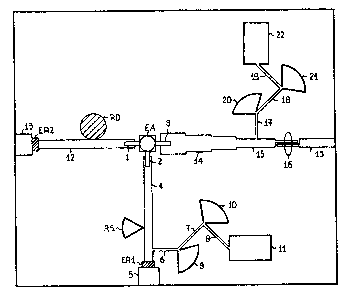
Referring to the drawing, an active device EA consists
for example of a field efect transistor (FET) with gate,
source and drain terminals, 1, 2 and 3. Source 2 ls con-
nected to a line 4 terminated in its characteristic im-
pedance by a resistive element ERl grounded to the under-
lying conductive layer through a pad 5. Close to resis-
tive element ERl, a filtering network composed of high
impedance lines 6, 7 and 8 and sector resonators 9 and 10
is connected to the line 4. This network communicates
with pad 11 which allows connection of the source bias
current supply.
Gate 1 is connected to a line 12, terminated by its
characteristic impedance using a resistive element ER2,
grounded through pad 13.
Drain 3 is connected through a three step impedance
transformer 14 to the output line 15, in which a coupled
line element 1~ is placed to block dc current. A filter-
ing network placed upstream of element 16, analogously
to that connected to the source, consists of lines 17,
18 19, sector resonators 20, 21 and pad 22. The drain
current generator is connected to this pad.
Oscillation commences due to positive feedback obtained
by loading gate 1 and source 2 with suitable reactances.
More particularly, in the case of source 2, a desired
reactance is produced by positioning in parallel to the
line 4 a microstrip resonator RS of the sector type,
placed at a suitable distance from the source and with
its axis orthogonal to line 4. It operates in first
approximation as a microstrip line with variahlP width
and length e~ual to ~/4, which transforms the open cir-
cuit at its end (defined by the curved side) into a
short circuit at the vertex in contact with line 4. The
electrical length of the t~u~ comprised between source
~8~
and sector RS is well defined, thanks to the limited
contact area between the sector and line.
The source load reactance required by the design is
obtained by appropriately dimensioning the trunk length
between the source and resonator RS.
The desired reactance at gate 1 is obtained by coupling
a dielectric resonator RD to line 12 at a suitable dis-
tance from the gate. This same resonator also stabilizes
the oscillation frequency. To a first approximation, an
open circuit is realized, at the resonance frequency of
RD, in the coupling section, i.e. in the section o~ line
12 identified by the diameter of the resonator orthogonal
to the line. sy suitably adjusting the distance of the
resonator from gate 1, the desired reactance is obtained.
Since the resonator RS has a comparatively low quality
factor Q, of the order of hundreds, and hence a compara-
tively wide band, synchronism with resonator RD is easily
attained and, accurate positioning of RD becom~ particu-
larly easy. On the other hand, although the Q of RS is
comparatively low, the short circuit-produced on line 4
has a very low resistive component since element RS is
in electrical contact with line 4. In consequence the
degree of positive feedback is optimized and high effici-
ency in terms of output power is obtained. At the same
time, all the advantages derived by damping of possible
undesired oscillation outside the working band are main-
tainsd. In fact such oscillation appears at frequencies
far from the working frequency (generally at very low
frequencies), at which the element RS is widely out of
3~ resonance and hence the source is loaded in a purely
resistive manner through line 4 terminated by the element
ERl.