Note: Descriptions are shown in the official language in which they were submitted.
~V~7~
CROSS-CONNECTION N~TWORK
USING TIME SWITCH
Background of the Invention:
_
The present invention relates to a
cross connection network for use in digital transmission
and in particular, to the cross-connection network for
S interchanging transmission paths of time division
multiplexed signals to one another in a station.
The cross connection network is for use in
initial route setting of transmission paths and change
of routes which are necessary on an increase of
transmission paths, change of services, and occurrence
of a fault
With an extension of available field of digital
communication, recent requirements are directed to a
reduction of size in a device, a decrease of a space for
laying cables, saving labor for cross connection, and a
variation of switchable hieratchy levels, in such a
cr-oss~connection network.
A conventional cross-connection network of the
type described uses a distribution frame comprising
switch groups switching mutual connection or cross
connection of a plurality of signal lines (for example,
5 coaxial cables) from one to another. The switches are
manually operated.
Such a digital signal transmitted on the
transmission paths is classified into two types one of
which is of a synchronous type and the other being of an
10 asynchronous type. For the digital signal of the
asynchronous type, a space division switch alone is used
to carry out cross connection of the signal lines as the
switch groups in the distribution frame because no
consideration is made about application of a time
15 division switch so as to interchange time slots from one
to another.
Such use of a space division switch in -the
cross-connection network results in difficulties of a
reduction of devices in size, saving the space for
20 laying the transmission cables, and a change of
switching units. Therefore, it is impossible to
completely respond to the above-mentioned recent
requirements.
~ore specifically, a restriction is imposed on
25 reducing the space division switch in size, although the
time division switch can readily be small sized by
integrating circuits.
In addition, it is necessary to switch
connections from one to another at every uni~ formed by
a lower order group by demultiplexing a higher order
group into a plurality of the lower order groups in
5 order to cope with a wide variety of switching units.
For this purpose, the conventional network comprising
the space division switch should comprise a
demultiple~er for demultiplex1ng the digital signals of
the higher order group into lower order groups which are
10 sent to the distribution frame. The network further
comprises a multiplexer for multiplexing the lower order
groups into a higher order group which is sent out from
the network. Thus, the cross-connection network
inevitably includes the multiplexer and the
15 demultiplexer in addi~ion to the distribution frame. In
order to transmit the demultiplexed digital signals of
the lower order group, signal lines are inevitably
increased in number. This makes a reduction of the
device and the collecting space impossible.
Summary of the Invention:
It is an object of the present invention to
provide a cross-connection network which can cross
connect bstween input and output lines by the use of a
time division switch in relation to asynchronous digital
25 signals.
It is another object of the present invention to
provide a cross-connection network of the type
described, which can reduce a d~vice in size and a line
laying space.
A cross-connection network has a plurality of
input lines and a plurality of output lines and is
5 operable in response to a plurality of input digital
signals incoming through the input lines, the input
digital signals having a first nominal bit rate in
common, so as to deliver the plurality of the input
signals to the output lines as a plurality of output
10 digital signals.
According to the present invention, the
cross-connection network comprises synchronizing means
responsive to the input digital signals for carrying out
pulse stuffing on the plurality of the input digital
15 signals at a second bit rate higher than the first bit
rate to produce a plurality of synchronized signals
synchronized with one another, each of which includes
signal bits for each of the input digital signals and
extra bits different from the signal bits, the signal
20 and the extra bits being arranged in time slots.
Multiplexing means is coupled to the synchronizing means
for multiplexing the plurality of synchronized signals
into at least one multiplexed signal, each of the at
least one multiplexed signal having a plurality of
25 frames assigned to the plurality of synchronized
signals, each of the plurality of frames having bit
signals in each one of the plurality of synchronized
signals assigned the~eto, each of the plurality of
~%~
frames being also assigned to the plurality of output
lines. Exchanging means is operable in a time division
fashion for exchanging -khe frames ~o one ano-ther in the
at least one multiplexed signal to produce at least one
5 exchanged multiplexed signals after exchanging the
frames. Demultiplexing means is coupled to the
e~changing means for demultiplexing the at least one
exchanged multiplexed signal into a plurality of
demultiplexed signals having the bit signals in the
10 frames, respectively. Destuff means is coupled to the
demultiplexing means for producing the plurality of
output digital signals by removing the extra bits from
said a plurality of demultiplexed signals, each one of
the plurality of plurality of output digital signals
15 being delivered to each one of said plurality of output
lines assigned with one of the frames corresponding to
the each one output signal.
Brief Description of the Drawings:
Fig. 1 is a block circuit view of a
20 cxoss-connection network according to a first em~odiment
of the present invention;
Fig. 2 is a view illustrating frame formats of a
pulse-stuffed signal and m multiplexed signals in the
network of Fig. l;
Fig. 3 is a view illustrating a frame format of
a multiplexed signal in a modification of a the network-
of Fig. 1
~L7~ 3l~3~
Fig. 4 is a view illustrating a multiframe
format of a D53 t signal which is formed by pulse
stuffing and multiplexing 28 asynchronous DSl signals;
Fig. 5 is a view illustrating a multiframP
5 format of another D53' signal which is formed by pulse
stuffing and multiplexing 28 synchronous DSl signals;
Fig~ 6 is a block circuit view illustrating an
interface according to another embodiment to produce
DS3' signal from 28 DSl signals;
Fig. 7 is a view illustrating a frame format of
another DS3' signal which is formed by pulse stuffing a
DS3 signal;
Fig. 8 is a block circuit view illustrating a
cross connector unit according to another embodiment;
Fig. 9 is a view illustrating formats of 34
parallel multiplexed signals in the cross connector unit
of Fig. 8;
Fig. 10 is a block circuit view illustrating a
cross-connection network according to another embodiment
20 o~ the present invention;
Fig. 11 is a view illustrating a format of a
stufed and multiplexed signal SM in the
cross-connection network of Fig. 10;
Fig. 12 is a view illustrating formats of m
25 parallel multiplexed signals in the cross-connection
network of Fig. 10;
Fig. 13 is a block diagram view illustrating an
embodiment of a local demultiplexer in Fig. 10;
3~
Fig. 14 is a block circuit view illustrating a
digital data smoothing circuit which is used for
destuffing extra bits in the cross-connection network of
the present invention; and
Fig. 15 is a view illustra-ting timing
relationships between various signals in the circuit of
Fig. 14.
Description o~ the Preferred Embodiments:
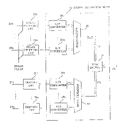
Referring to Fig. 1, a cross-connection network
10 according to a first embodiment of this invention is
connected between first through n-th input lines 201 to
20n and first through n-th output lines 211 to 21n,
where n is a natural number greater than unit~.
Supplied with first through n-th input digital signals
15 through the first through n-th input lines 201 to 20n,
the cross-connection network is operable to assign the
first through n-th input digital signals to the first
through n-th output lines 211 to 21n in response to a
connection control signal CC. The first through n-th
20 input digital signals have a common nominal bit rate fo
and are delivered to assigned ones of the first through
n-th output lines 211 to 21n. Such input digital
signals may be a low order group of, for example, DSl
having the bit rate of 1.544 MHz (or 1.544 Mb/s). The
25 first through n-th output lines 211 to 21n are given
irst through n th output digital signals each of which
has a bit rate fo equal to the nominal bit rate fo.
The first through n-th input diyital signals are
sent to firs~ through n-th pulse stuff~ng circuits 221
to 22n each of ~hich is similar in structure and
operation to one another. Description will be therefore
5 made about the first pulse stuffing circuit 221, alone~
In the first pulse stuffing circuit 221, pulse
stuffing is carried out on the first input digital
signal by the use of a sequence of internal clock pulses
having an internal bit rate fs greater than the nominal
10 bit rate fo. As a result, the first stuffiny circuit
221 successively produces a first pulse stuffed signal
which is sub~ected to the pulse stuffing and which has a
predetermined format specified by a succession of
frames. It is assumed that each of the frames is
15 composed of m bits (m being integer).
The remaining pulse stuffing circuits 222 to 22n
are operated in the above-mentioned manner and produce
second through n th pulse stuffed signals which are
synchronized with -the first local synchronized signal
20 and which have the same bit fs rate as the latter. The
first through n-th pulse stuffing circuits 221 to 22n
may collectively be called a pulse stuffing unit while
the first through n-th pulse stuffed signals may
collectively be referred to as a pulse stuffed signal.
Temporarily referring to Fig. 2, each of the
first through n-th pulse stuffed signals is led by frame
pulses as shown along a first line of Fig. 2~ and has
each of the frames that is composed of first through
~ ,7~
m-th bits bl to bm, as illustrated along a second line
of Fig. 2. The first through m-th bits bl to bm of the
frame are composed of a plurality of extra bits, such as
a frame bit, at least one stuff bit/ and a stuff control
5 bit, in addition to one of the first through n-th input
digital signals.
In Fig. 1, a cross-connector unit 25 comprises
first through n-th serial--to-parallel (S/P) converters
261 to 26n supplied with the first through n-th pulse
10 stuffed signals, respectively. The first through n-th
pulse stuffed signals are subjected to S/P conversion by
the first through n-th S/P converters 261 to 26n and
converted into first through n-th parallel signals each
of which is composed of m bits. Thus, the S/P
15 conversion is carried out at every frame of m bits. The
first through n-th parallel signals are sent to a
multiplexing circuit 28 at every frame.
The multiplexing circuit 28 multiplexes the
first through n-th parallel signals into m parallel
20 multiplexed signals MU as shown in Fig~ 2. More
specifically, the first bits of the irst through n-th
pulse stuffed signals are depicted at bl(l), bl(2), ..
bl(n) and are successively arranged in a time division
fashion as shown along the third line of Fig~ 2. Such a
25 time divisional arrangement of bl(l), bl(2), ... bl(n)
may be called a first group. Likewise, the second bits
b2(1), b2(2), ... b2~n) are arranged in the time
division fashion synchronized with first bits bl(l),
~,~t~
bl(2), ... bl(n), as shown along the fourth line of Fig.
2, and will be referred to as a second group. While,
the m-th bits bm(l), bm(2), ... bm(n) are arrang~d in
the above-mentioned manner to form an m th group. Thus,
5 m parallel multiplexed signals are produced to have the
first to m-th groups, respectively.
From this fact, it is readily understood that
the multiplexing circuit 28 multiplexes first through
m-th bits of the fir~t through n-th parallel signals at
10 every bit, respectively. This means that first through
m-th bits in i-th one of the first through n-th ~/P
converters 261 to 26n simultaneously produce in first
through m-th parallel multiplexed signal, respectively,
and j-th bit in the first through m~th bits in the i-th
15 one can be depicted at bj(i), where j is a natural
number between 1 and m, both inclusive.
The multiplexed signals MU are sent to a time
switch 31 and are switched under control by the
connection control signal CC which is given from a
20 common controller 32 in the known manner. The
connection control signal is indicative of interchange
of the bits or time slots arranged in each of the m
parallel multiplexed signals MU. As a result, the
connection control signal CC indicates the interchange
25 of first through n-th ones of the time slots in each of
first through m-th groups. Therefore, the time switch
31 interchanges the first through n-th time slots in the
first through m-th groups and produces first through
11
m-th interchanged parallel signals CH. Each of the
first through m-th parallel signals CH is composed of
first through n-th bits as a resul-t of multiplex in the
multiplexer 28 but time slots are interchanged according
5 to the connection control signal CC. The firs-t through
n-th bits of each of first through m-th interchanged
signals CH are demultiplexed by the demultiplexer 33 and
distributed to first through n-th P/S converters 341 to
34n, respectively. Thus, first through n-th P/S
10 converters 3~1 to 34n receive first through n-th m-bit
parallel signals, respectively, and supply first through
n-th destuff circuits 351 to 35n with first through n-th
serial signals each of which composed of m bits
Each destuff circuit 351 to 35n establishes
15 frame synchronization and thereafter removes the extra
bits to produce the first through n-th output signals
which are reproduction of the first through n-th input
digital signals appearing as a result of the interchange
of the time slots. The first through n-th output
20 signals are delivered to the first through n-th output
lines 211 to 21n, respectively.
As mentioned above, the first through n-th input
digital signals, even if they are asynchronous to one
another, are subjected to pulse stuffing to ~orm first
25 through n-th pulse stuffed signals which are
synchroniz~d to one another. The pulse stufEed signals
are multiplexed in a time divisional fashion. This
enables interchange of the time slots by the time switch
31 and cross-connection or delivery of ~he first through
n-th input signals to the n output lines 211 to 21n,
respectively, as desired. Accordinyly, it is possible
to reduce a switch for cross connection in size and to
5 save a cable laying space in comparison with the
conventional network. In addition, it is possible to
rapidly switch routes for cross-connection from one to
another only by the use of the connection control signal
CC .
In the illustrated example, the S/P converters
261 to 26n and the P/S converters 341 to 34n are
included in the cross-connector unit 25 so as to adjust
a bit ra-te (namely, fs x (n/m)) of the multiplexed
signals MU to be equal to a switching rate of the time
15 switch 31. However, such converters 261 to 26n and 3~1
to 34n may be removed from the cross-connector unit 25
when the time switch 31 is operable at a bit rate of (fs
x n).
In no use of the S/P converters 261-16n and the
20 P/S converters 3~1-3~n, pulse-stuffed signals from pulse
stuffing circuits 221-22n are multiplexed at the
multiplexer 28 and are formed to a multiplexed signal
comprising first through n-th frames serially arranged
as shown in Fig. 3. The first through n-th frames are
25 composed of frames in the pulse stuffed signals from the
first through n-th pulse-stuffing circuits 221-22n,
respectively.
13
The first switch 32 interchanges time slots to
interchange a plurality of frames to one another by the
connection control signal CC and produces an
interchanged multiplexed signal wherein frames are
interchanged to one another~ The interchanged
multiplexed signal is demultiplexed at the demul-tiplexer
33 and the resultant multiplexed signals are applied to
destuff circuits 351-35n, respectively.
Now, description is made as to an example where
n = 28 and the input digital signals are DSl signals
(1.544 Mb/s).
The twenty-eight input DSl signals are pulse
stuffed at pulse stuffing circuits 221-22n and are
multiplexed to a multiplexed signal having a frequency
fh' of 45.808 MHz which will be called DS3' signal~
A pulse stuffing ratio ~ is determined by the
following equation (1):
L' (fh' - N' fo) -(fo H' - NL')
f h . . . ( 1 )
where I.' is number of bits of one DSl signal assigned to
one frame (which is equal to m in Figs. 2 and 3), H'
being number of entire bits in a multiframe, fo being a
frequency of a signal to be pulse stuffed (DSl = 1.544
MHz), N being a multiplicity (= 28).
When L' = 204 and therefore H' = 204 x 28 =
5712, the multiplexed signal DS3' has a format as
depicted in Fig. 4.
14
ReEerring to FigO 4, each frame comprises a
first bit for a frame pulse F, data bits 1-193, vacant
bits Vl-V6, stuff control bits Cl-C3, and a parity bit
P. These first through 28th frames are arranged
serially as shown in Fig. 3.
When twenty-eight input DSl signals are
synchronized with each other, a format of the
multiplexed signal should be determined by the following
equation (2) in addition to equation (1) because data
bit arrangement of a digroup in each of input DSl
signals should be maintained as it is:
fo x N x (L' - ~)
f ' = - - ...(2)
where ~ is a variable of a frame length and a simple
rational number and Dl is a frame length of one diqroup.
The digroup is a piece of data bits of 24
channels each of which is composed of eight data bits
and one digroup comprises one-handred and ninety-three
(193) bits.
The format of the multiplexed signal is as shown
in Fig. 5. Each of the first through 28-th frames
comprises a first bit for a frame pulse F, and data bits
1-193, Digroups of the first through 28th DSl signals
are distributed in the first through 28th frames,
respectively. After data bits, there are assigned
signal bits Sl-S4, Sa, and Sb for future use, vacant
bits Vl-V3, and a parity bit P at ~he last bit.
~.~7B~
In use of the forrnat of Fig. 5, the input DSl
signals are completely synchronized with the multiplexed
signal DS3' by providing a vacant frame comprising
two-handreds and four (204) vacant bits once per
5 four-handreds and nine (409) frames.
When number of input lines are a multiple of
twenty-eight (28) and when DSl signals income through
the input lines, the input DSl signals can be classified
into a plurality of sets each comprising t~lenty-eight
10 DSl signals, so that each set of twenty-eight input DSl
signals is processed to produce DS3' signal comprising
the format as depicted in Figs. 4 or 5 in dependence on
whether or not twenty-eiyht input DSl signals are
synchroni~ed with one another by use of an interface as
15 shown in Fig~ 6.
Referring to Fig. 6, the interface shown therein
comprises a pulse stuffing circuit for pulse stuffing
twenty-eight DSl signals incoming through twenty-eight
input lines Il-I28. The resultant twenty-eight pulse
20 stuffed signals have respective frame formats shown in
Fig. 4 or Fig. 5. The pulse stuffed signals are
supplied to a multiplexer 36 which comprises a data
storage 37 and a controller 38.
The pulse stuffed signals are temporarily stored
25 in the data storage 37 and are read out from the data
storage 37 by controller 38 in the order of the frame
numbers 1-28. Accordingly, the frames 1-28 are serially
arranged one after another to form a multiplexed signal
which is sent out from the controller as the DS3'
signal. Then, resultant multiplexed signals comprising
the format in Fig. 4 and/or Fig. 5 are further
multiplexed and then applied to the time switch (31 in
Fig. 1~. Cross connection can be carried out by
interchanging frames to one another by the time switch.
When each of the first through n-th input
digital signal is a signal having 44.763 Mb/s which will
be called DS3 signal and when it is pulse stuf~ed to
0 DS3' signal, a pulse stuffing ratio p is determined by:
fo x H'
f h
where H is number of bits in each DS3 signal to be
assigned in a subframe in DS3' signal and H' is a number
of all bits in one frame of DS3' signal.
Fig. 7 shows a format of one frame of DS3'
signal. The one frame comprises 28 subframes and each
subframe comprises a first bit for frame pulse F, data
bits 1-200, and control bits Cl and C2 a-t 51th and 103rd
bits, and a parity bit P at the last bit. Those first
to 28th subframes are serially arranged to form a frame
and similar n frames for n input DS3 signals are
arranged as shown in Fig. 3 by multiplexing those DS3'
signals corresponding to n input DS3 signals.
Referring to Fig. 8, an embodiment of the cross
connector unit 25 is shown for one-handred and
twenty-eight (128) input DS3' signals depicted at Il to
I12~. The input signals Il to I128 may be considered as
17
the pulse stuffed signals synchronized with one another.
Each signal has a forma-t as illustrated in Fig. 7.
The first through 128th DS3' signals Il to I128
are divided into first and second incoming groups which
5 are composed of the first through the sixty-fourth DS3'
signals Il to I64 and the sixty-fifth DS3' signals I65
to I128, respectively, and which are specified by
s~mbols A and B, respectively. In the illustrated
cross-connector unit 25, the first and the second
10 incoming groups ~ and s are delivered to first and
second S/P converter and multiplexer units 30A and 30s,
respectively.
In the first and second 5/P converter and
multiplexer units 30A and 30B, the DS3' signals Il to
15 I64 and I65 to I128 of each incoming group A and B are
converted into first through 204th parallel bit signals
A(1-204) and s(l-204). Each set of the first through
204th bit signals is composed of bits in a subframe in a
single one of the DS3' signals.
The first through 204th parallel bit signals of
each incoming group A and B are classified into, for
example, first through sixth subyroups each of which is
composed of thirty-four bit signals as depicted at
A(1-34), A(35-68), ... , A(171-204), B(1-34), B(35-68),
25 ... , B(171-204) in the figure. In each subgroup, the
corresponding bits in successive subframes are arranged
in the order of the subframes to form thirty-four rows
each having 28 bits and corresponding subgroups in
~'~7~
18
si~ty~four signals in each of incoming group A ~nd B are
serially arranged to form thirty-four parallel
multiplexed signals as illustrated in Fig. 9 in
connection with, for example, A(1-34). ~ 34) are also
5 represented in the same format and therefore "B(1-34)"
is labelled with parentheses in Fig. 9.
In Fig. 9, bll represents a first bit in first
subframe and generally bij represents a j-th bit in an
i-th subframe, and each of symbols Il to I64 (I65 to
10 I128) used for representing frames implies that the bit
elements in the frame are included in an input DS3'
signal represented by the same symbol.
The multiplexed signals of first through the
sixth subgroups of the first and the second incoming
15 groups are sent to a time switch 31 which comprises
first through sixth switch units 411 to 416.
More particularly, the 34 parallel multiplexed
signals of first subgroups A(1-34) and s(l-34) of the
first and the second incoming groups A and B are
20 delivered to the first switch unit 411 through a pair of
buses each of which is composed of thirty-four lines.
Likewise, the second through the sixth subgroups of the
first and the second incoming groups ~ and B are
delivered to the second through the sixth switch units
25 412 to 416, respectively.
Inasmuch as the first through the sixth switch
units 41] to 416 are similar in structure and operation
to one another, description will be made about the first
v
19
switch unit 411 as a representative of the illustrated
switch units 411 -to 416.
The first switch unit 411 comprises a
multiplexer 42, first and second static random access
5 memories (SRAM) 43 and 44, a selector 45, and a
demultiplexer 46. The multiplexer 42 multiplexes each
one of the parallel multiplexed signals of the first
subgroup Atl-34) and each one of the parallel
multiplexed signals of subgroup s(l-34) at a
10 multiplicity equal to two by interleaving bits of the
both multiplexed signals.
The resultant signals are stored in one of two
SRAMs 43 and 44 and are stored in the other after the
former is stored full. Reading operation is carried out
15 from one SRAM 43 or 44 to which storing operation is not
being carried out. The selector 45 selects one of SRAMs
43 and 44 from which reading operation is permitted
The reading operation is performed under control
of the connection control signal CC (FigO 1) and frame
20 interchange is performed between some of frames Il to
I64 and I65 to I128 in Fig. 9. The read out signals are
arranged in a form similar to the signal multiplexed by
interleaving at multiplexer 42, and are demultiplexed at
demultiplexer 46. Then, switch unit 461 produces
25 thirty-four parallel signals (1-34)A of subgroup A and
another thirty-four parallel signals (1-34)B of subgroup
B similar to those of in Fig. 9 but having interchanged
frame or f rames.
~7~
In all of the other switch units 412 to 416,
input signals are processed in the similar manner and
produce processed signals as depicted at (35-68)A,
(35-68)B, ..., (171-204)A and (171-204)B in the figure.
5 In this connection, A and B imply subgroups A and B,
respectively.
The cross connector unit 25 of this embodiment
further comprises demultiple~er and P/S converter units
32A and 32B which process input signals in a manner of
10 reversed processes as processes in S/P converter and
multiplexer units 30A and 30B.
The produced signals (1-34)A and (1-34)B are
supplied to demultiplexer and P/S converter units 32A
and 32B, respectively, from first switch unit 411.
15 Similarly, signals of subgroup A and and signals of
subgroup B from switch units 412 to 416 are supplied to
demultiplexer and P/S converter units 32A and 32B,
respectively. Those input signals are processed at
respective demultiplexer and P/S converter units 32A
20 and 32B to reproduce the DS3 ' sigrlal5 which are sent out
to respective lines 01 through 0128. Thus, the input
DS3' signals on input line Il to I128 are delivered to
output lines 01 to 0128, respectively, depending to
frame interchange at time swi-tch 317
It will be easily understood that the cross
connector unit of Fig. 8 can be applied to cross connect
DS3' signals as descrihed in connection with Figs. 4 and
5.
~ ~t7
21
In the present embodiment, increase or decrease
of input and ou-tput lines can be readily performed
without expansion of unit size. When input and output
lines are increased by 28, another S/P and P/S
5 converters are added and are connected to added input
and output lines, respectively~ The S/P and P/S
converters are connected to time switch 31 though
respective 3~ buses in the similar manner described~
Then, the multiplexer 42 in each switch unit 41 is
10 adjusted to have a multiplicity of 3.
Referring to Fig. 10, a cross-connection network
according to another embodiment of this invention is
supplied through the first through n-th input lines 201
to 20n with first through n-th asynchronous input
15 digital signals each of which is of a high order group
of, for example, DS3 having a bit rate of 44.736 Mb/s.
In this connection, the illustrated cross-connection
network comprises first through n-th pulse stuffing
circuits 221 to 22n which comprise first through n-th
20 local demultiplexers 511 to 51n and first through n-th
stuff and multiplex circuits 521 to 52n, respectively.
The first through n-th local demultiplexers 511
to 51n serves to demultiplex the first through n-th
input digital signals o the high order group into first
25 through n-th local demultiplexed signals, respectively.
Each of the first through n~th local demultiplexed
signals LDl to LDn is composed of first through k-th
~q~7~
partial signals of a low ~rder group of, for example,
DSl.
The fi.rst. through n-th local demultiplexed
signals LDl to LDn axe sent to the first through n-th
5 stuff and multlplex circuits 521 to 52n, respectively.
In each of the first through n-th stuff and multiplex
circuits 521 to 52n, the first through k-th partial
signals are pulse stuffed and mu].tiplexed into a
stuff/multiplex signal in synchronism with each frame
lO pulse~
It will be easily understood that each of the
stuff and multiplex circuits 521 to 52n can be arranged
similar to the interface of FigO 6.
Referring to Fig. ll, each stuff/multiplex
l5 signal is divisible into a succession of frames each of
which is composed of firs-t through m-th units. Each of
the first through m-th units is composed of first
through k-th bits which can collectively be represented
by bji, where j is an integer between l and m, both
20 inclusive and i represents another integer between l and
k, both inclusive. Accordingly, j-th one of the first
through m-th units are composed of the first through
k-th bits bjl to bjk. This shows that a single one of
the frames is formed by multiplexing the first through
25 k-th partial signals each of which has a length of m
bits. In this event, extra bits, such as a stuff bit
and a frame hit, are included in m bits.
~_ ~t~
In Fig. 10, firs-t through n-th stuff/mul-tiplex
signals SMl - SMn are sent from khe first through n-th
stuff and multiplex circuits 521 to 52n to the cross
connector unit 25 in synchronism with the common frame
5 pulses. Therefore, the first through n th
stuff/multiplex signals have frame beginning time
instants which simultaneously appear to define the
fxames.
The cross connector unit 25 is operable in a
10 manner similar to that illustrated in conjunction with
Fig. 1. More particularly, the first through n-th
stuff/multiplex signals SMl - SMn may be subjected to
S/P conversion by the use of S/P converters 261 to 26n
(Fig. 1), and are multiplexed into m parallel
15 multiplexed signals MU by the multiplexer 28 (Fig. 1).
The m parallel multiplexed signals have formats as shown
in Fig. 12 wherein n first units U2(1) - Ul( ) are
arranged in the first multiplexed signal, n second units
U2~1) - U2(n) being in second multiplexed signal, and n
20 m-th units Um(l) - Um(n) being in m-th multiplexed
signal. Thereafter, the m multiplexed signals MU are
sent to the time switch 31. The ~ime switch 31
interchanges ox exchanges time slots in each of the
multiplexed signals MU to interchange a plurality of
25 units to one another to produce first through m-th
interchanged signalsO Each of the first through m-th
interchanged signals has a multiplexed format similar to
Fig. 12 but units being interchanged to one another.
~'7~
24
The first through m-th interchanged signals are
demultiple~ed a-t demultiplexer 33 (Fig. 1) and are
subjected to P/S conversion at first through n-th P/S
converters 341-34n (Fig. 1). The converted signals have
5 the format similar to Fig. 10 and are delivered to first
through n-th destuff circuits 351 to 35n, respectively.
In the example being illustrated, the first
through n-th destuff circuits 351 to 35n comprise first
through n-th destuff/multiplex circuits 531 to 53n and
10 first through n-th local multiplex circuits 541 to 54n,
respectively. Each of the first through n-th
destuff/demultiplex circuits 531 to 53n estahlishes
frame synchroni~ation and removes to extra bits from
each P/S converted signal. Thereafter, each
lS interchanged signal is demultiplexed into first through
k-th digital signals of the low order group. The first
through k-th digital signals are multiplexed at each
local multiplex circuit of 541-54n into an output
digital signal of the high order group~ Such output
20 digital signals are sent as first through n-th output
signals from the first through n-th local multiplex
signals 5~1 to 54n through the first through n-th output
lines 211 to 21n, respectively.
Thus, each of the first through n-th output
25 digital signals carries the first through ~-th partial
signals of the low order group which are arranged in
each input digital signal.
As mentioned above, each input digital siynal of
the high order group is stuffed and multiplexed after it
is demultiplexed into a plurality of digital signals
each of which is of a low order groupO Therefore, the
5 low order group signals are synchronized to one another.
Under the circums-tances, the interchang~ or exchange of
the time slots is carried out by the time switch to
interchange high order group signals and the
interchanged high order group signals are sent to the
10 first through n-th output lines, respectivelyn
Since cross connection is thus completed by use
of the time switch, it is possible to reduce the networ~
in size, and to save a cable laying space, and to
rapidly switch routes from one to another by the use of
15 the connection control signal CC.
In Fig. 13, an example of one of local
demultiplexer in Fig. 10 is shown together with an
associated stuff and multiplex circuit. The local
multiplexer and the stuff and multiplex circuit are
20 depicted at 51 and 52.
In the example being illustrated, the input
digital signal of the high order group, namely, DS3
having the bit rate of 44.736 Mb/s is ~upplied to local
demultiplexer 51 through the input line 20 (suffix
25 omitted) and the stuff and multiplexer 52 serves to
supply the cross connector unit 25 (Fig. 10) with a
rearranged signal which can be interchanged or exchanged
by the time switch 31 (Fig. 1) and which may be of the
26
high order group DS3' having a format as shown in Fig. 4
or 5.
Referring to Fig. 13, the local demultiplexer 51
comprises a first demultiplexer portion 61 and a second
5 demultiplexer portion 62 between the first demultiplexer
portion 61 and the stuff and multiplex circuit 52.
Supplied with the input digital signal DS3, the
first demultiplex portion 61 demultiplexes the input
digital signal DS3 into first through seventh
10 demultiplexed signals each of which is composed of a
lower order group, namely, DS2 and which have a bit rate
of 6.312 Mb/s. Therefore, the first through seventh
demultiplexed signals will be collectively represented
by DS2(1) to DS2(7)o The first through seventh
15 demultiplexed signals are also destuffed at the
demultiplexer portion 61.
The first through seventh demultiplexed signals
DS2(1) to DS2(7) are sent to first through seventh
demultiplex units 621 to 627 of the second demultiplex
20 portion 62 together with first internal clocks CLKl of
6.312 Mb/s. Each of the first through the seventh
demultiplex units 621 to 627 demultiplexes and destuf~s
each of the fir~t through the seventh demultiplexed
signals DS2(1) to DS2(7) into four subsidiary
25 demultiplexed signals each of which is of a lower order
group, namely, DSl having a bit rate of 1.544 Mb/s and
which is destuffed. Therefore, the subsidiary
demultiplexed signals may be referred to as DSl group
~i7~
signals. ~s a result, first through twenty-eighth ones
of the subsidiar~ signals are produced from the first
through the seventh demultiplex uni-ts 621 to 527 in
synchronism with second interval clocks CLK2 of 1.544
5 Mb/s and may be represented by DSl(l) to DSl(28),
respectively.
The first through twenty-eighth subsidiary
signals DSl(l) to DS1(28) are delivered to the stuff and
multiplex circuit 52 together with the second clocks
10 CLK2. The stuff and multiplex circuit 52 carries out
to pulse stuffing on, and multiplexing of, the first
through twent~-eighth subsidiary signals by use of a
third internal clock CLK3 having a bit rate of 45.736
Mb/s to form the DS3' signal having the frame multiframe
15 format as shown in Fig. ~.
In Fig. 14, an example of a destuff circuit
shown therein is a, so called, digital data signal
smoothing circuit and is cored in the cross connection
system of the present invention so as to remove the
20 extra bits such as frame pulses, stuff pulses, stuff
control pulses, vacant bits and others in a digital data
signal.
Referring to Fig. 14, the smoothing circuit
comprises a data signal input terminal 71 and a clock
25 input terminal 72. The data input terminal 71 receives
a digital data signal ds (ds in Fig. 15) having a bit
rate of fn. The clock input terminal 72 receives a
clock pulse cp having the bit rate fn.
28
The clock pulse cp is supplied to a frequency
divider 73 which, in turn, dividers khe clock pulse cp
to produce first through third frequency divided pulse
signals pl, p2, and p3 (pl, p2, and p3 in Fig. 15).
The clock pulse cp is also applied to a first
clock generating circuit 74 which generates a burst
clock signal bc from the clock pulse signal cp under
control of the first pulse signal pl. The burs~ clock
generating circuit 74 comprises an OR gate having two
10 input terminals to which the clock pulse signal cp and
the first pulse signal pl are applied, respectively.
Accordingly, the clock pulse signal cp is permitted to
pass through the OR gate only for a time duration of a
pulse of the first pulse signal pl and a burst clock
15 signal bc is obtained on an output of the OR gate. The
pulse duration of the first pulse signal pl is
determined a time period over M (integer) successive
clock pulses per N (integer N ~ M) successive clock
pulses. Thereforel the burst clock signal bc 11
20 comprises M successive clock pulses repeatedly
generating each interval of N successive clock pulses~
The digital data signal ds is applied to a burst
data signal generating circuit which is composed of a
flipflop (F/F) circuit 75. The digital data signal ds
25 is reformed by the F/F circuit 75 in synchronization
with the burst clock signal bc which is applied to the
F/F circuit 75. Therefore, the F/F circuit 75 produces
a burst data signal bd (bd in Fig. 15) in response to
29
the burst clock signal bc. That is, sorne, that i,s M
data bits, of successive N data bi~s in the digital data
signal ds are repeatedly derived as the burst data
signal bd and the remaining data bits are removed~
The burst data signal bd is applied to a first
shift register 76 under control of the burst clock
signal bc. The first shift register 76 comprises M F/F
circuits 761-76M connected in cascade.
Output signals of the F/F circuits 761-76M are
10 supplied in parallel to one another to a selector unit
77 which comprises M selectors 771-77M. The selectors
771-77M operates in response to the second pulse signal
p2 to supply the output signals from the F/F circuits
761-76M to a second shift register 78. The second shift
15 register 78 comprises o-th through M-th F/F circuits
780-78M which are connected in cascade through selectors
771-77~.
In absence of the second pulse signal p2, each
selector of 771-77M connects between adjacent two F/F
20 circuits connected to each other through the selector~
The third signal p3 is applied from the
frequency decider 73 to F/F circuits 780-78M.
Therefore, the M data bits in the second shift register
78 are serially sent out from the last stage F/F circuit
25 78M as an output data signal do.
The third pulse signal p3 has comprises
succession pulses with a bit rate of fn x M/N and a
pulse of the second pulse signal p2 has a pulse width
equal to one bit of the third pulse signal p3. The
pulse of the third pulse signal p3 is generated at the
end of each one pu15~ of the first pulse signal pl.
In the example shown in Fig. 14, N and M are
5 selected 5172 and 17. However, N and M can be
determined as desired.