Note: Descriptions are shown in the official language in which they were submitted.
~7~
~U~TIPROC~SSOR SYST M
BACKGK3~D 0~ THE IN~E~lTION
The present in~ention relates to a multi-
processor system, more particularly to a multi-
processor system suitable for use in an electronic
switching system.
Electronic switching systems may, for example, be
roughly divided into network portions ~Jhich actually
perform the circuit switching or packet switching and
processor portions which manage the network portions and
perform call processing control. The present invention
particularly relates to the latter processor portion.
This processor portion may fundamentally be
a single processor, but when the electronic switching
1~ system is large in scale, the network portion also
becomes large and, correspondingly, a plurality of
processors are introduced. These processors include
several secondary processors and a main processor for
exercising overall control over the secondary pro-
2~ cessors, which all together make up a single multi-
processor system. To improve the reliability of the
multiprocessor system, the technique of duplexing is
introduced. That is, the constituent elements (pro-
cessors and buses) are duplexed into a O system (active
system) and 1 system (standby system), with one backing
up the other.
The above method of system construction is based
on the so-called "one-machine concept", and is extremely
flexible with regard to changes from a single processor
3~1 to multiple processors and further to a duplex construc-
tion. For example, it is an extremely efficient method
of coping with enlargements of scale of private branch
exchanges (PBX). Therefore, it is considered that such
multiprocessor systems will come into wide use in the
~!
~ 27~331~
future.
As explained above, for duplexed multipro~essor
systems, in an electronic switching system, there are
single manayement processors (the aforemèntioned main
processors) and pluralities of call processors (the
aforementioned secondary processors for call
processing) all of which processors are duplexed. In
such a case, the switching of systems among the 0
system and 1 system processors is an important
operation. In the past, the method used for this
system switching operation was to grant the right to
system switching to the call processors. In other
words, any call processor could select the o system or
1 system.
According to the conventional method for system
switching of the duplexed multiprocessor system, for
the order of control among the call processors and the
management processors, the software had to be managed
each time the call processors exercised the system
switching rights. In the end, this resulted in the
disadvantage of complicating the software management.
SUMMARY OF THE I~ENTION
In accordance with an embodiment of the present
invention ~here is provided a multiprocessor system
comprising: pluralities of secondary processors; a
first main processor connected so as to govern and
manage a first plurality of the secondary processors;
a second main processor connected so as to govern and
manage a second plurality of the secondary processors;
a first system bus, including a control bus and a
communication bus, connected to the first main
processor and to the first plurality of secondary
processors; a second system bus, including a control
bus and a communication bus, connected to the second
main processor and to the second plurality of
secondary processors; the main processors, the
.~
s~condary processors and the system buses are
duplexed, and one of a first system including the
first main processor, the first plurality of secondary
processors and the first s~vstem bus, and a second
system including the second main processor, the second
plurality of secondary processors and the second
system bus is an active system and the remaining one
of the first and second systems is a standby system;
two first means, respectively connected to each other
and to a corresponding one of the first and second
main processors, for controlling system switching by
issuing system switching signals and second means,
respectively connected to a corresponding one of the
first means and to a corresponding one of the first
and second pluralities of the secondary processors,
for switching between the active system and the
standby system, each second means is activated in
response to at least one of the system switching
signals issued by the corresponding one of the first
.0 means.
In accordance with another embodiment of the
present invention there is provided a multiprocessor
system, comprising: two main processors each having an
active state and a standby state; a plurality of
secondary processors, wherein each of the main
processors is associated with a corresponding
plurality of the secondary processors; two system
buses, connected between respective ones of the main
processors and the corresponding plurality of
secondary processors, each of the system buses having
an active state and a standby state, and each of the
system buses including a control bus and a
communication bus; wherein each of the main processors
controls the corresponding plurality of secondary
processors, so that no direct communication is
possible between the secondary processors; two first
means, respectively connected to each other and a
~27~
corresponding one of the main processors, for system
switchlng and provlding an instruction command and a
notification command to the corresponding secondary
processors; and two second means, respectively
connected to a corresponding one of the first means,
for system switching from an active state to a standby
state, each of the second means being activated by the
instruction command.
BRIEF DESCRIPTION OF THE DRAWINGS
The above and other features of the present
invention will become more apparent from the following
description of the preferred embodiments with
reference to the accompanying drawings, wherein:
Fig. 1 is an explanatory view illustrating a
basic multiprocessor system according to the present
invention;
Fig. 2 is an explanatory view o~ the
multiprocessor
3a
~%7~3f~B
system according to a first embodiment of t'ne present
invention;
Fig. 3A shows an example of the components of t'ne
system to which the ~resent invention is applied on t~e
secondary processor side;
Fig. 3B shows an example of the components of t~e
system to wnic'n the present inven~ion i~ applied on the
main processor side;
Fig, 4 shows schematically the method of
lo system switching of the present invention according to a
first embodiment;
Fig. 5A shows specific examples of the system
switching instruction units of the present invention for
the management processor (i.e, MPR) side;
Fig. 5B shows examples of system switching display
units of the call processor (i.e. CPR) side related with
the system switching instruction units of the present
invention;
~ig. 6A shows examples of management processors
provided with system switching notification units
according to the present invention;
Fig. 6B shows examples of call processor groups
activated by the system switching notification units of
Fig. 6A;
~5 Figs. 7A to 7D show the system transition in the
case of power-on initial process loading IPL;
Figs. 8~ to 8D show the system transition in
the case of a management processor MPR fault;
Figs. 9A to 9D show the system transition in the
case of an IPC fault in an MPR at IPL;
Figs. loA to loD show the system transition in the
case of an IPC fault in a CPR in IPL;
Figs. 11A to llD show the system transition in the
event of an emergency supervisor equipment ESE
emergency;
Fig. 12 is an explanatory view of the multi-
processor system according to a second embodiment of the
present invention; ~ ~7~3~8
Fig. 13 shows scnematically the metnod or system
switchins of the present invention according to the
second embo~iment;
Fig. l~A shows an example of the flow of opera-
tion of the system switching prediction in the
second embodiment;
Fig. 14B shows an example of the operational flow
of a system switching request in the second embodiment;
o Fig. 15A shows examples of management processors
provided with firs-t holding units according to the
second embodiment;
Fig. 15s shows examples of call processors
provided with second holding units according to the
second embodiment;
Figs. 16A to 16D show the system transition
upon zero phase (i.e. PHO) restart;
Figs. 17A to 17D show the system transition in
the case of a fault in the IPC of a CPR;
~o Figs. 18A to 18D show the system transition in the
case of a fault in the IPC of the MPR; and
Figs. l9A to 19D are views of system tran-
sitions in the case of a fault in a call processor CPR.
DETAILED DESCRIPTION OF THE PREFERRED EMBODIMENTS
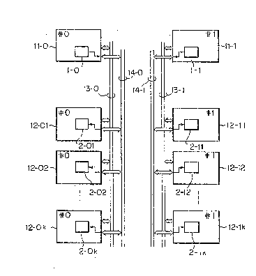
Figure 1 is an explanatory view illustrating a
basic multiprocessor system according to the present
invention. In the Figure, 11-0 is a 0 system main
processor and 11-1 a 1 system main processor, each
governing and managing a plurality of 0 system secondary
processors 12-01 to 12-Ok and a plurality of 1 system
secondary processors 12-11 to 12-lk, respectively.
Among these processors are connected 0 system and 1
system communication buses 13-0 and 13-1 for principally
transferring data. Further, among these processors are
connected 0 system, and 1 system, system-control buses
14-0 and 14-1 principally for the transmission of
~`~
~27~3~3~
control signals. Here, co~,straint is ~pplied so that
all the processors of the O system and all the buses of
the O system send and receive data ~nd control signals
in the O system only, and a]l the p~oces60rs of the 1
system and al] the buses of the 1 system send and
receive data and control signals in the 1 system only.
This is a precondition of the present invention, ~n
other words, communication is only possible among
elements of the same system, By constraining com-
l~ munication to be only among elements of the same system
in this way, the amount of hardware can be considerably
reduced and the software management can be made con-
siderably easier.
Another important precondition is that the secon-
dary processors (12) not be given any system switching
rights and that only the main processors (11) exercise
system switching rights, This can overcome the afore-
mentioned problem of the prior art.
Further, the present invention includes two
means. The first means 1-0, 1-1 for achieving system
switching control are mounted in the O system and 1
system main processors 11-0 and 11-1, respectively. The
second means 2-01 through 2-Ok for executing the system
switching are mounted in the O system secondary pro-
~5 cessors 12-01 through 12-Ok, respectively. Also~ the
second means 2-11 through 2-lk for executing the system
switching are mounted in the 1 system secondary process-
ors 12-11 through 12-lk, respectively. Each of the
second means (2) is activated in response to a command
given from the first means (1).
Figure 2 is an explanatory view of the multi-
processor system according to a first embodiment of the
present invention. In the first embodiment, the first
means 1-0 and 1-1 of Fig. 1 respectively include both O
system and 1 system system switching instruction trans-
mission units 15-0, 15-1 and both O system and 1 system
~, 6
~2~7~33~3
system switc~ing notification units 16-0, 16-1.
The O system and 1 system, system switching
instruction units 15-0 and 15-1 are provided inside the
main processors 11-0 and 11-1, respectively, and unc-
tion to send commands, i.e., system switc'ning instruc-
tions from the main procesjors 11 (0 system and 1
system) to the secondary processors 12. The signals for
the switching instructions are transferred through the
system control buses 14-0 and 14-1 connected to the main
o processors 11 on the other hand, the system switching
notification units 16-0 and 16-1 are also in the main
processors 11-0 and 11-1 and notify the secondary
processors 12 that a system switching instruction has
already been sent from the system switching instruction
units 15-0 and 15-1 It should be understood that the 1
system communication bus 13-1 and the 1 system control
bus 14-1 are not illustrated specifically for simpli-
fication, but these buses are in parallel with the O
system communication bus 13-0 and the O system control
bus 14-0, respectively, as shown in Fig. 1.
Assume now that the O system is the active
system For some reason, (for example, a fault),
the maln processor 11-0 performs switching of the
system. Thereby, the 1 system main processor 11-1
subsequently operates as the active system There-
fore, due to the above preconditions, the 1 system
secondary processors 12-11 to 12-lk and the 1 sys-
tem buses 13-1 and 14-1 become the active system.
At this time, the system switching instruction unit
15-0 sends a system switching instruction signal to
the corresponding O system secondary processors 12-
01 to 12-Ok and the system switching instruction
unit 15-1 sends a system switching instruction
signal to the corresponding 1 system secondary pro-
cessor 12-11 to 12-lk. Next, the O system pro-
cessors (12-01 to 12-Ok)~ display that they should
~27~
become the standby system. conversely, the 1
system processors (12-11 to 12-lk), display that
they should become the active system TheSe
displays are made by the O system, sys~em-switching
display units 17-01 tO 17-Ok and the 1 systeM,
system-switching display units 17-11 to 17-1~ in
Fig. 2, HoWever, these display units need not be
newly provided because use may be made of existing
flag registers or status registers.
Therefore, a system switching instruction is
sent from the main processor 11 side to the secondary
processor 12 side. The secondary processors, however,
cannot immediately detect t'nat their own statuses have
been changed. Therefore, the active system and standby
system on the main processor 11 side and the active
system and standby system on the secondary processor 12
side invert, leading to serious system errors. Gener-
ally, the switching instruction cannot be immediately
detected because the system switching display (17),
includes the above-mentioned flag or status registers,
is not looked at while the secondary processors 12 are
on-llne. They are looked upon at most when the power is
turned on or upon IPL (initial program loading).
Therefore, it is arranged so that the system
switching notification units 16-0 and 16-1 notify
without delay the O system and 1 system secondary
processors 12-01 to 12-Ok and 12-11 to 12-lk that system
switching has occurred and prompt the processors to look
at their internal switching display units (17). At this
point, the active system and standby system of the main
processor 11 side coincide with the active system and
standby system of the secondary processor 12 side.
Figure 3A shows an example of the components
of the system to which the present invention is applied
on the secondary processor 12 side. Figure 3B shows an
example of the components of the system to which the
,~
33~
present invention is applied on the main processor 11
side. Particularly important constituent elements of
the present invention lie ln the blocks shown by CC and
CSC in Fig. 3A and in the blocks shown by CC, MSC, and
ISC in Fig. 3s (discussed in detail late~). Note that
the following explanation is rnade in refe~ence to the
example of an electronic switching system, but the above
main processors 11 are specifically management proces-
sors 12 and the above secondary processors are speci-
lo fically call processors. In the Figures, the former are
illustrated as MPR (management processors) and the
latter by CPR (call processors). In Fig. 3A, the call
processors CP~a to CPRk control the corresponding
networks NWa to NWk. The networks include speech path
memories and other switching system functional units and
set a path route. The existence of a plurality of
networks ~a to ~W~ is based on the so-called ~load
dispersion~ rationale. For this, a plurality of call
processors CPRa to CPRk are provided corresponding to
the networks.
Further, to improve the reliability of commu-
nication, the networks are duplexed and thus include O
system (#O) and l system (#l) pairs. The O system call
processor (CPR) group communicates through the communi-
cation bus 13-0 with the O systern management processor
MPRo. In accordance with need, the O system call pro-
cessors (CPRao to CPRko) can also communicate with each
other through the communication bus 13-0. In the same
way, the active system, i.e., the 1 system call proces-
sor (CPR) group communicates through the communication
bus 13-1 with the 1 system management processor MPRl
and, in accordance with need, the 1 system cal~ pro-
cessors (CPRal to CPRkl) communicate with each other
through the communication bus 13-l. It is assumed here
3s that in any one of the processors CPR, communication
between CPR's within a system is performed (#0~___#1),
~d ~J ~
but communication between systems wit~ ot'ner cPR's is
not performed. This is for simplification of the
hardwaLe and simolification of the software management,
Next, an explanation will be made of the internal
construction of the call processors CPR, All of the
call proc~ssors CPR have the same construction, so t'ne
explanation will be made of CPR as a typical ~xample,
The 0 system and l system of the call processor CPRa
comprised of CC, ISC, CSC, IPC, and M~. The names of
o these parts are shown below:
(l) CC: Central controller
(2) ISC: Interface subsystem controller
(3) CSC: ca]l processor side system recon-
figuration controller
(4) IPC: Inter multiprocessor communicator
(5) MM: Main memory
(6) PBS: Processor bus
Among the above (l) to (6), (1), (5), and (6) are
general elements~ while (2), (3), and (4) are elements
unique to the multiprocessor system. First, looking at
the interface subsystem controller ISC, the controller
interfaces between the 0 system and l system. In pre-
paration for system switching, the controller supplies
to the standby system the data of particular import~nce
contained in the latest data of the active system. when
system switching occurs, it functions so that the stand-
by system can be set up quickly.
The call processor CPR side system reconfiguration
controller CSC is on the call processor MPR side (there
is also one on the management processor side) and trans-
fers control information for control of reconfiguration
through the system control bus (14) when there are
faults making system reconfiguration impossible, upon
power on, etc. on the normal communication route in the
multiprocessor system.
The inter multiprocessor communicator IPC is a
~%7~
control device for performing data communication
operations on the cor~munication bus (13) from the CPR' â
to an MPR, from an MPR to the CPR's, or among cPR's of
the same system. That is, data communication for the
usual call processing is performed through this communi-
cator IPC.
Next, an explanation will be made of the internal
construction of a management processor ~PR in reference
to Fig. 3B. ~owever, no repetition will be made of the
lo explanation of blocks the same as those explained with
reference to Fig. 3A. Note that the buses 13-0, 13-1,
1~-0, and 14-1 of Fig. 3B are completely the same as the
buses 13-0, 13-1, 14-0, and 14-1 of Fig. 3A. The blocks
unique to Fig. 3B are as follows:
(1) MSC: Management processor side system
reconfiguration controller
(2) IBC: Inter multiprocessor bus controller
(3) PBC: Peripheral bus controller
The above-mentioned management processor side
system reconfiguration controller MSC is placed on the
management processor side and functions the same as the
call processor side CSC.
The inter multiprocessor bus controller IBC
controls the right to use of the communication bus (13)
by the inter multiprocessor communicator IPC which, for
example, performs polling. Further, the peripheral bus
controller PBC controls the input-output controller IOC
and functions as an adapter for the external memory
devices (floppy disks etc.) under the IOC. Note that
the block connected with the management processor MPR by
the dotted line is a debug console D-CNS and is used
only during software debugging.
Therefore, the plurality of call processors CPR of
Fig. 3A and the management processors MPR are used to
control the plurality of networks NWa to NWk. In such a
system, the present invention relates to how the system
11
switc~ing is perEormed. For exarnple, "hen t~lere is a
fault in a CPR in t~e active system, i.e , 0 ~stem
(~o)~ control is passed to the standby system, i.e., the
1 system (~1), by the designated p~-ocedure.
Flgure 4 s'nows schematically the met'nod of system
switc~ing of the present invention according to t~le
first embodiment. In the Figure, ~e portion above t'ne
communication buses 13-0 and 13-1 is the 0 systern and
the portion below is the 1 system, the two systems being
lo shown separated. IPC are inter multiprocessor communi-
cators, already explained with reference to Figs. 3A and
3B, an IPC connecting the management processor MPR#0 and
the call processors CPRa#0 to CPRk#0 through the com-
municatlon bus 13-0. Exactly the same construction
applies to the 1 system as shown. In the Figure, CPU is
a central processing unit and a general name for the
elements in the MPR's and CPR's, other than the IPC's,
in Fig. 3A and Fig. 3B (that is, CC, ISC, MM, etc.) and
are grouped together for the sake of simplification of
illustration. The CPU's of the 0 system are connected
by the system control bus 14-0, while the CPU's of the 1
system are connected by the system control bus 14-1. As
with the system control buses 14, there are shown the
system switching instruction signal lines SS (SS-0 and
SS-l) and the system switching notification signal lines
ST (ST-0 and ST-l), which are of particular relevance to
the present invention.
As a precondition of the present invention, it
is considered that the instruction Eor system
switching is given primarily by the management pro-
cessors MPR. Therefore, system switching instruc-
tion signal lines SS are used and the system
switching instruction performed uniformly for the
call processors CPRa to CPRk. In this case, the
system switching instruction is given simultan-
eously not only to the system originating the system
~L~ 3 3 ~ ~3
switching instruction, but alao to the ot~er systern.
Such intersystem liaison is per~ormed tnroug'n
the line Ll. Here, the system switching disp:Lay
units 17 of the CPRis (block referenced by 17 in
Fig. 2) are given new system displays. Tha~ is,
those previously displa~ed as the 1 syatem (0
system) are given a display to the ef~ect that they
are to be changed over to the 0 system (1 system)
Next, a system switching notification signal is
lo sent from the management processor MPR side to the call
processor CPR side For -this, system switching
notirlcation signal lines ST are used. Here, the CPR's
are instructed to look at the corresponding system
switching display units (17). under this instruction,
the CPR'S operate as the new system In this case, the
switching notification is given simultaneously not only
to the system originating the system switching instruc-
tion, but also to the other system, with the intersystem
liaison being performed through the line L2, in a
similar fashion to the above-mentioned system switching
instruction.
Figure 5A shows specific examples of the system
switching instruction units 15 of the present invention
for the MPR side. Figure 5B shows examples of system
switching display units 17 of the CPR side related to
the system switching instruction units 15 of the present
invention The constituent elements of Fig. 5A and Fig.
5B are connected by the 0 system, system-switching ins-
truction signal line SS-0 and the 1 system SS-l. In
Fig. 5A, the side left of the center is the 0 system and
right of the center is the 1 system. That is, the
management processors MPR-0 and MPR-l are arranged to
the left and right. Their constituent central con-
trollers CC-0 and CC-l, interface subsystern controllers
ISC-0 and ISC-l, and system reconfiguration controllers
MSC-0 and MSC-l are shown. The system switching
13
. .
~7~
instruction units (15-0 and 15-l in Fig. 2), which ar-
characteristic features of the present invention, a~e
shown as 15-0 and 15-l in the interface subsystem
controllers ISC-0 and Isc-l. A cross-connection line Ll
is used to form a kind of latch circuit. ~,1 is
equivalent to the line Ll shown in Fig. 4. This cross-
connection makes it possible to ensure that lf one side
is the 0 system, the other side necessarily becomes the
l system The output logics instructing the 0 system
lo and l system, for example, ~0~ and ~l", are sent through
the respective corresponding drivers DRV-O and DRv-l (or
DRV-l and DRV-O ) to the system switching instruction
signal lines SS-O and SS-l (or SS-l and SS-0). The
signal lines SS-0 and SS-l are one of the system control
buses 14-0 and 14-l, respectively. The buses 14-0 and
1~-l are connected by the connectors CN-0 and CN-l to
the MP~-0 and MPR-l.
The system switching instruction units 15-0 and 15-
1 are driven, upon the detection of some fault by the
management processor MPR of the active system. Sup-
posing that MPR-O is the active system, an example of
the events until the driving of the system switching
instruction unit 15-0 is explained below. Note that the
explanation will be only for the 0 system, since the
same events apply equally as well in the case where the
l system MPR-l is the active system. Further, the
system-switching instruction unit 15-l is driven
automatically through the line Ll by the other system
switching instruction unit 15-0. According to this
example, first, the fault detection timer FDT-0
overflows. In general, the timer FDT is managed by
software and is programmed so that the count is cleared
every fixed period of time. That is, so long as no
abnormalities arise, such as a runaway operation of the
software, etc., the timer FDr will be cleared and thus
will not overflow. If it overflows, this means that
14
'~1~
~L%7~3~3
some sort of abnormality has arisen, so t'ne over~lo~
information is set through the gates Gl-o and ~2-C to
the predetermined bit EA of the emergency r gister RG
0. sy this change o~ the bit EA, the 0 system, system-
s-witching ins-truction unit ]5-0 is driven through the
emergency timing circuit EMAT~M and from there a sys~em-
switching instruction signal SssO is output. The signal
SssO is sent to the system-switching instruction signal
line SS-0, as already explained. At the same time, the
1 system, system-switching instruction unit inverts in
status. Furt'ner, the predetermined bit A/S in the mode
register RG2-0 of 0 system switches to S. A of the A/S
bit means the active system and S the standby system.
Therefore, the A/S bit of the mode register RG2-1 in the
1 system is switched frorn S to A. Note t'nat A/S are
differentlated by merely the difference between the
logic ~ or ~0~. Therefore, a switching instruction is
sent from the management processor MPR-0 to the 0 system
call processors CPRa to CPRk. Further, switching is
simultaneously proceeded with in the 1 system MPR-l,
also by the switching information obtained from the line
Ll, and a switching instruction is sent to the 1 system
call processors CPRa to CPRk as well. Note that the
reasons for faults are not limited to the above. Many
reasons exist and other reasons are notified mutually
through the cross-connection line L'l. EMASUP in the
Figure is an ~'emergency-action suppress~ signal The
factor ESE (emergency supervisor equipment), which is to
be set simultaneously in the 0 system and 1 system, is
set in a predetermined bit in the above-mentioned
emergency regis-ter RGl, through the 0 system and ].
system one-shot circuits SHT-0 and SHT-l. However, the
above-mentioned ESE, EMASUP, FDT, etc are not the main
point of the present invention and thus will not be
explained in detail.
The system switching instruction signals SssO and
~7~33813
Sssl rrom the above system s~itc'ning instruction units
15-0 and i5-1 are supplied to the call processor CPE
side, so the explanation will be continued with
reference to Fig. ~3. In Fig. 5B, the C~Ra 0 and CPRa 1
are respectively the 0 system and ~ system call pro-
cessors (CPRa). The same applies ror CPRk. In the
CPRa 0, there are included the central controller CCa 0
and sys~em reconfiguration controller CSCa 0. The game
applies for the CPRa 1~ CPRk_o~ and CPRk 1 C
o in the same system are connected through the connec-
tors (CN) in a series fashion (in the Figure, ~R is a
terminal resistance). In the cen-tral controllers, cc
there are previously established mode registers, pre-
determined bits A/S which include the afore-mentioned
system switching display units 17 (in the Figure, 17a-o,
17a-1 to 17k-o, 17k-1). The meaning of A/S (Act/
Standby) was explained with reference to Fig. 5A. In
the above example, the 0 system functioned as the active
system, so the A/S bits of the system switching display
units 17 of the 0 system and 1 system are, respectively,
'~0~' and "1'~. If a fault is detected by the management
processor MPR-0, the system switching instruction
signals SssO and Sssl become the logic "1" and ~0~,
respectively, by the procedure explained with reference
to Fig. 5A and are taken into the 0 system call pro-
cessor CPR group and 1 system call processor group CPR
to change the logic of the A/S bits. However, it is
impossible with this alone for the call processors CPR
to switch themselves to the other system (active standby
system, standby active system). The reason being is
that when the call processors CPR are on-line, they do
not look at the mode registers. Therefore, the aEore-
mentioned system switching notification units 16-0 and
16-1 are activated. ThiS will be explained below.
Figure 6A shows examples of management processors
MPR provided with system switching notification units 16
16
~27~3~3a~
according tO the present invention Figure 6B shows
examples o' call processor groups ac~ivated ~y the
systern switching notification units of Fig. 6A.
Constituent elements of Fig, 6A and Fig. 6B are con-
nected by the O system, systern-control bus 14-0 an~ the
1 system, system-control bus 14-1. Among these, the O
system and 1 system, system-switching notification
signal lines ST-O, ST-l and ST'-O, ST'-l are the
respective synchronization signal transmission lines.
lo Note that the line L2 in Fig. 4 corresponds to the line
L2 for mutual connection in Fig. 6A. In this Figure,
the system switching notification units 16-0 and 16-1 of
the present invention are in the management processor
MPR side system reconfiguration controllers MSC-O and
MSC-l and specifically are realized as EM bits in the
emergency action designation registers EADR-O and EADR-
1. When ~ stands in an EM bit, it means that an
abnormality has occurred. Note that writing into an EM
bit is performed by software processing. ThiS ~ of an
~0 El~ bit is sent as the system switching notification
signal SsTO (if the 1 system, SsTl) through the driver
gate DG to the system switching notification signal line
ST-O. At this time, the EM bit "1" is supplied through
the line L2 to the opposing system (1 system) as well.
~5 In the 1 system, notification of the occurrence of
system switching is received through the system
switching notification signal line ST-l.
In actuality, not only is the system switching
notification signal (EM bit, S~TO, SsTl) but also a
synchronization clock signal must be sent. This clock
signal is sent as the synchronization signal CLO,
whereby synchronization is established among the system
reconfiguration controllers CSCa 0, CSCa 1 to CSCk 0,
and CSCk 1 which receive said system switching noti-
-
fication signal SsTO, SsTl. Note that if the 1 system
is the active system, the synchronization signal CLl is
17
used. In either case, the siynals are generated by the
synchronizati~n signal generation circuits ~I,G-~ and
CLG-l and transmitted by the synchronization signal
cransmission lines ~T' 0 and ST'-1 to the call processor
CPR side. on the call processor CF~ side of Fig 6B,
the system switching notification signals SsTO, '5s~rl and
the synchronization signal CL0 (Cr,l) are received at the
system reconfiguration controllers CSCa 0, CSCa 1 to
CSCk 0, and CSCk 1 If the 1 system, respectively, had
o been the active system up to then, SsTl and CLl would be
received by the CSC's of -the two systerns. These signals
preferably set predetermined bits MEM (management pro-
cessor emergency), in the existing restart flag regis-
ters (RSFR-O and RSFR-l ) in the central controllers (CC)
to '~ at a predetermined timing. This timing is
defined by the afore-mentioned synchronization signal
CL0.
Notification of system switching in this way to the
CPR 'S through the restart flag registers (RSFR) is
extremely effective. The reason for this is that the
restart flags are for instructing interruption of
highest priority, so the software in the call processors
(CPR ) immediately looks at the predetermined bits. At
that point in time, the system switching display units
(17) of Fig. 5B, that is, the A/S bits, are looked at
and processing started for switching to the other
system, whereupon the active system is switched to the
standby system and the standby system to the active
system. At this point, it is realized that everything
in the 0 system is to be switched to the standby system
and everything in the 1 system is to be switched to the
active system.
Several examples of the operation achieved in the
first embodiment will be given.
(1) power-on IPL (initial program load)
(2) Fault in MPR: PHl
18
3~3~
(3) Fault in IPC in MPR at IPL: PH2
(4) Faul-t in IPC in CPR at IPL: P~2
(5) ESE emergency: PHl
The meanings of tne abo~e symbols, other than PHl
and P~2, have already been explained. p~ means '~phase"
It is usually divided into 0, 1, and 2, tne higher the
number, the higher the degree of fault. That is, PH2
indicates the highest level and requires the highest
priority.
lo In an electronic switching system, in the Prd2 set-
up mode, the exchange processing itself cannot be
maintained. In PHl, there is a sudden switching despite
the system being on-line, but current communication can
be saved while dialing is cut off. In PH0 switching,
current communication can be saved and dialing can be
saved, so t'ne conversing parties will hardly notice
anything in this set-up mode.
Figures 7A to 7D show the system transition in the
case of power-on IPL. The order of transition is, from
the top, 7A -~7B -~7C--~7D. The transition charts are
drawn according to the system construction of Fig. 4.
In the lines connecting the MPR ' s and CPR ' s, no special
operation occurs on the dotted line portions; action
occurs only on the solid line portions. The same is
true for the following Figs. 8 to 11. The solid line in
Fig. 7A is a PH2 activation message, which PH2
activation message is sent from an MPR to all the cPR's.
The solid line in Fig. 7B is a reply to the P~2 activa-
tion message, this reply to the PH2 activation messaye
is received by the MPR from all the CPR ' s, whereby
initial program loading IP~ of the CPR ' s occurs and
restart processing performed. In Fig. 7C, ~ indicates
intersystem data communication and ~ exchange proces-
sing (data communication). At ~ , an MPR begins an M~
copy operation from all the CPR's of the ACT (active)
system to the ssY (standby) system. At ~ , in parallel
19
~7~
wit~ this copy operation, the sys-tem enters exchange
processing (on-line processing) in a parallel rnode
Figures 8A to 8D show the system trans.tion in the
case of an MPR fault. In Fig. 8A ~ indicates exchange
processing and 2 intersystem data communication. The
multiprocessor system is in normal operation (on-line~,
but the A/S (AcT/ssY) bit is rewritten by the emergency
circuit. In Fig. 8B, ~ indicates an MPR side emer-
gency (~EMA) and ~ a P~l ac-tivation message. At ~ ,
o the occurrence oE a fault in an MPR is notified from the
MPR to all the CPR's. At ~ , a PHl activation message
is sent frorn the MPR ~o all the CPR's. The solid line
in Fig. 8C is a reply to PHl activation message, the
reply to PHl activation message reply being received by
the MPR from all the CPR's, whereby restart processing
is performed at the system PHl. In Fig. 8D, at ~ , the
CPR's read a fault hopper of the old ACT system at the
end of the P~l restart processing and, when there is
nothing written there, perform the above copy operation.
At ~ , the MPR reads the CC switching flag of the old
ACT system at the end of the PHl restart processing and,
when there is nothing written there, goes down alone.
Note that ~ indicates exchange processing tdata
communication).
Figures 9A to 9D show the system transition in the
case of an IPC fault in an MPR at IPL. In Fig. 9A, a
PH2 activation message is sent from the MPR to all the
CPR's. Note that ~MC indicates an emergency counter
which counts the number of occurrences of emergencies.
In Fig. 9B, at ~ , the MPR emergency circuit is
activated by -the absence of a PH2 activation message
reply from all the cPR's. At ~ , execution of the
system PHl is attempted (by MPR), but since no program
is loaded, the software runs wild and, as a result, the
FDT again overflows. In Fig. 9C, ~ indicates an MPR
side emergency, wherein the IPC fault in the MP~ under
:.
-
IPL is notified from the MPR to all the CPR's. At ~ ,
a P~2 activation message is sent frorn the MPR to all the
CPR's. In Fig. 9D, at ~ , the MPR emergency circui~ is
activated by the absence of a PH2 activation messaye
reply from all ~he CPR's. ~ indicates a .~PR side
emergency M~MA, wherein an IPC fault in the MP~ is
notified from the MPR to all the cPR's. At ~ , a PH2
activation message is sent from the MPR to all the
CPR's. At ~ , the same process is performed at the
power-on IPL shown in Fig. 7.
Figures 13A to lOD show the system transition in
the case of an IPC fault in a CPR under IPL. The solid
line in Fig. lOA is a P~2 activation message, the P~2
activation message being sent by an MPR to all the
CPR's. In Fig. loB~ at ~ , the MPR receives the P~2
activation message reply from all the CPR'S. At ~ , as
receipt of communication from the CPR is impossible,
the emergency circuit is activated (FDT is made to
overflow). At ~ , the MPR tries to execute the system
PHl, but since no program is loaded, the software runs
wild and the FDT overflows. In Fig. lOC, ~ , indicates
an MPR side emergency MEMA, wherein the IPC fault in the
CPR under IPL is notified from the MPR to all the CPR'S.
At ~ , a PH2 activation message is sent from the MPR to
~5 all the CPR'S. In Fig. lOD, at ~ , the MPR emergency
circuit is activated by the absence of a PH2 activation
message reply from all the CPR's. ~ indicates a MPR
side emergency MEMA, wherein an IPC fault in the CPR is
notified from the ~PR to all the CPR'S. At ~ , a PH2
activation message is sent from the MPR to all the
CPR's. Thereafter, at ~ , the same process is per-
formed at the power-on IPL shown in Fig. 7.
Figures llA to llD show the system transition
in the event of an ESE emergency. In Fig. llA, ~
indicates the occurrence of an ESE emergency (El~A). At
, the MPR emergency circuit is activated, the ESE bit
21
~.`
of the ~PR emergency r~gister ~G turns O~l, and a ~esta~t
is issued. At the same time as the restart, A/S
switching is performed and thus an ESE emergency (EMA)
is issued. Therefore, the ESE bits of the two systems
turn o~. In ~ig. llB, ~ indicates an I~PR side emer-
gency, wherein the occurrence of an ESE emergency in the
CPRa is notified from the MPR to all the CPR'S. ~t
a PHl execution message is sent by the MP~ to all the
CPR's. The solid line in Fig. llC is a reply to a p~l
o execution message, and P~2 is an execution message reply
which is received by the MPR from all the CPR'S. The
solid line in the system of Fig. llD is a p-~l execution
message with an independent down request. First, the
ESE, bit of the MPR register RG is looked at and the
occurrence of ESE ~A discerned. Next, the PHl
execution message with the independent system down
request is sent to all the CPR ' s. Finally, the MPR and
all the CPR's assume system down independently
As explained in detail above, according to the
first embodiment of the present invention, respective
duplexed multiprocessors can execute switching from the
0 system to 1 system or vice versa without the software
management becoming complicated and without the intro-
duction of complicated hardware. Use for an electronic
switching system results in much greater effectiveness
of the system.
The reasons for a system switching are, as
mentioned previously, principally faults, but include
other factors as well. For example, there are periodic
switchings. llPeriodic switchings" are system proces-
sings for ensuring the stability of the standby system,
wherein every fixed period of time (for example, at
night), the active system and standby system are
compulsorily switched to actively discover potential
faults. In this case, system switching is requested
even though there i5 no actual fault. In such system
.~
~7B~
switching, an extremely large amount of data has to be
transferred from the active system to the starld'Dy system
and the problem of a lony time being required is pre-
sent. Further, even if the instruction for system
switching is sent from t'ne main processors 11 to the
secondary processors 12, it ta'~es tirne for the editing
of the data of the instruction and the decoding on the
receiving side, and therefore the resolution of these
problems has become increasingly difficult. The same
lo thing applies in the case of transfer o~ control
information from the secondary processors 12 to the main
processors 11. If the system switching request from the
secondary processors 12 to the main processors ]1 is
control information, it takes a considerable amount of
time for control information to be understood at the
main processors 11. If the system switching from the
secondary processors 12 derives from a serious fault,
there is the problem that the time lag will cause a
major fault in the system. This problem can be overcome
by a second embodiment of the present invention, which
will be explained in detail below.
Figure 12 is an explanatory view of the multi-
processor system according to a second embodiment of the
present invention. In the second embodiment, major
members are identical to those recited in the afore-
mentioned first embodiment. That is, 11-0 is the O
system main processor and 11-1 the 1 system main pro-
cessor, each governing and managing a plurality of O
system secondary processors 12-01 to 12-Ok and a
plurality of 1 system secondary processors 12-11 to 12-
lk, respectively. Among these processors are connected
O system and 1 system communication buses 13-0 and 13-1
for principally receiving data (for simplification, the
1 system communication bus 13-1 is not shown, but is in
parallel with the O system communication bus 13-1).
~,
~7~3~3
Further, among these processors are laid ~ system and 1
system control buses 14-0 and 14-1 principally for the
transmission of control signals (for simplification, ~he
O system control bus 14-0 alone is shown, but the 1
system control bus 14-1 is in parallel r~ith 14-0).
Here, constraint is applied, as in the ~irst embodiment,
so that all the processors of the O system and all the
buses of the O system only receive data and control
signals in the O system and all the processors of the 1
lo system and all the buses of the 1 system only receive
data and control signals in the l system. This is a
coMmon precondition of the present invention. In other
words, communication is only possible among element:, of
the same system. By constraining communication to be
only among elements of the same system in this way, the
amount o~ hardware can be considerably reduced and the
software management can be made considerably easier.
Another precondition is that the secondary processors
(12) not be given system switching rights. In
~O principle, the main processors (ll) exercise system
switching rights. This enables the software management
to be made considerably easier.
Based on the above, in a multiprocessor system
constituted in the second embodiment, a prediction
~5 signal SpO (Spl in the case of the l system being the
active system) is sent from the main processor (11) side
as to predict to the secondary processors 12 that system
switching is going to be executed in the future. The
prediction signal SpO is received via the system control
bus 14-0 and held in the O system, second holding units
22-01 to 22-Ok in the secondary processors 12-01 to 12-
Ok
on the other hand, a request signal Sro is sent
from one of the secondary processors 12-01 to 12-ok to
the main processor 11-0 for execution of system
switching between the active system and standby system.
24
This signal is sent frorn the secondary processo~ 12
which recognizes that a ~ault has occurred the-rein and
indicates communication is impossible. The same applies
for the 1 system. A request signal srl is sent from the
1 system secondary processor with a fault through the
system control bus 14-1 to the main processor li-I.
Assume no~ that the 0 system ia the active sy,tem. For
some reason, for example, due to the afore-rnentioned
periodic switching, the rnain processor 11-0 schedules
lo swltching oE the system to 11-1. This is predictable
since it is a switching defined in the software.
Therefore, the secondary processors 12 of the two
systems are given a prediction to the effect that there
will be system switching. This is the prediction signal
Sp.
This enables system switching work, begin prin-
cipally the transfer of data to the 1 system,
before the periodic switching instruction is sent
to the secondary processors 12 and thus enables the
periodic switching to be made in an extremely short
time. In this case, the secondary processors 12
supervise periodically the second holding units
(22) therein (~look-in~) to read the instruction
status (~status read~
on the other hand, the processor system engages in
system switchings, fundamentally, with the main pro-
cessors (11), so faults in the secondary processors 12
would not allow the secondary processors 12 to change
over the system as a whole without the main processor
11. Therefore, the secondary processors (12~ are made
to send request signals Sr for system switching to the
main processors (11) and thus the main processors 11-0
and 11-1 are provided with a 0 system first holding unit
21-0 and a 1 system first holding unit 21-1 the
same as the above second holding unit (22) so as to
hold the request signals Sr. In this case, the main
.,i
~L~ 3 3 ~
processors 11-0 and 11-1 periodically supervise t~eir
internal first holding units 21-0 and 21-1 (~loo~-in"
to read their instruction statuses (~status read").
Syscem switching is started speedily with just t~e
simple transfer of a signal Sr. Note that it is nct
~nown at the main processors 11 from w'nich secondary
processor 12 the request signal Sr was issued However,
in system switching, no matter where the fault, the
result is the same, i.e a fault has occurred.
lo Therefore, first, the system is switched, then sub-
se~uently, and slo~ly, the appropriate secondary pro-
cessor 12 can be determined by periodic tests etc. Note
that it is not necessary to provide new first and second
holding units (21, 22) because use can be made of exis-
ting flag registers or status registers.
Comparing Fig. 12 (second embodiment) with Fig. 1
(basic structure), the first means 1-0 and 1-1 (Fig. 1
for achieving system switching control corresponds to
the O system and 1 system, first holding units 21-0 and
~0 21-1, respectively. The second means 2-0 and 2-1 (Fig.
1) for executing system switching correspond to the O
system and 1 system, second holding units 22-0 and 22-1.
For a detailed example of the elements on the
secondary processor 12 side of the second embodiment,
see Fig. 3~, relating to the first embodiment. For a
detailed example of the elements on the main processor
11 of the second embodiment, see Fig. 3B, relating to
the first embodiment.
Figure 13 shows schematically the method of system
switching of the present invention according to the
second embodiment. In the Figure, major parts are
identical to Fig. 4. The portion above the communica-
tion buses 13-0 and 13-1 is the O system and the portion
below is the 1 system, the two systems being shown
separated, IPC indicates the inter multiprocessor
communicator, already explained with reference to Figs.
y:,
-s ~,
3A and 3B, the IPC connecting the management processor
MPR~0 and the call processors CPRa#0 to CPRk~0 throuyn
the communication bus 13-0. Exactly the same construc-
tion applies to the 1 system as shown In th~ Figure,
the cen~ral processing units CPU's are general names for
the portions in the MPR's and CPR's, other than the
IPC's, in Fig. 3~ and Fig. 3B (that is, CC, ISC, ~M,
etc.) and are grouped together for the sake OL' simpli-
fication of illustration. The CPU's of the 0 system are
lo connected by the system control bus 14-0, while the
CP~'s of the 1 system are connected by the system
control bus 14-1. As with the system control buses,
there are shown the system switching predic-tion signal
lines SP (SP-o and SP-l) and the system switching
request signal lines SR (SR-0 and SR-l), which are of
particular relevance to the second embodiment.
As a precondition of the first and second
embodiment, it is considered that the instructions for
system switching are performed primarily by the manage-
ment processors MPR. Therefore, a system switching
prediction signal line SP is used and the system swit-
ching prediction is performed uniformly for the call
processors CPRa to CPRk. Here, the second holding units
(blocks referenced by 22 in Fig. 12) of each CPR are
given a new system display. That is, those previously
indicated as the 1 system (0 system) are given a display
to the effect that they should be switched to the 0
system (1 system). After this, the required system
switching is begun at the CPR'S.
on the other hand, when system switching is
requested due to a fault in the call processors CPR,
s1nce as a precondition of the present invention the
instruction for system switching is handled primarily by
the management processors MPR, the request is made by
the transmission of tne request signal Sr through the
system switching request signal line SR to the main
r~ 27
,~L~
processors ~PR. In this case, the first holding units
of the MPR's (blocks referenced by 21 in Fig. 12) are
given a new system display. That is, those previously
indicated as the 1 system (o system) are given a disp1ay
requesting a switching to the 0 system (1 system).
After this, the requir~d system switching is begun for
the whole system.
Figure 14A shows an example of the flow of
operation of the system switching prediction in
lo the second embodiment. Figure 14B shows an example
of the operational flow of a system switching
request in the second embodiment. First, looking
at Fig. 14A, the central controller CC in the mana-
gement processor MPR of the active system (for
example, before periodic switching) transfers a
system switching prediction signal Sp to the mana-
gement processor side system reconfiguration con-
troller MSC of the MPR. Next, the signal Sp is
transferred on the system control bus and reaches
the call processor side system reconfiguration
controller CSC of the CPR's. Next, it is held by
the second holding units 22 therein. Next, the
CPR's supervise the second holding units 22 by
'llook-in'~ to read the status display by ~status
~5 read~. In this case, this is a prediction of a
system switching and the previously explained
corresponding operation is started. According
to an example of the second embodiment, a ~phase zero,
PH0" instruction is used as the prediction signal Sp.
This is convenient in use. Phases are usually
classiEied into 0, 1, and 2, the greater the number
indicating the greater the degree of fault. That is,
PH2 is the highest level and requires processing of
highest priority.
In an electronic switching system, in the PH2 set
up mode, the exchange processing itself cannot be
~;7B3~
maintained. In PHl~ there is a sudden switching despite
the system being on-line, but current communication can
be saved while dialing is cut off. In a PH0 switching,
current communication can be saved and dialiny can 'oe
saved, so the conversing parties will hardly notice
any.hing in this set up mode However~ in the PH0
switching, a large amount oE data must be transferred in
a short time, in advance, to the standby system, which
is crucial to a switching operation. A typical example
o of this PH0 switching is the aforementioned periodic
switching.
Looking now at Fig. 14B, first, when a central
co~troller CC in a call processor CPR of the active
system detects by itself a fault in a portion other than
the CC, since communication is impossible, it quicl~ly
gives a system switching reques~ signal Sr to its
internal call processor side system reconfiguration
controller CSC and transfers it to the management
processor side system reconfiguration controller MSC of
the MPR through the system control bus 14. However, it
is assumed that there is no abnormality on the transfer
bus of the signal Sr in the CPR. (The case where the
signal Sr itself cannot be transferred is not touched
upon by the present invention, but sooner or later the
fault of the CPR would be detected by the MPR due to the
lack of a reply signal, e-tc.) The request signal Sr,
upon reaching the MSC of the MPR, is held by the first
holding unit 21 therein. Next, the MPR supervises the
first holding unit 21 by ~look-in~ to read the status
display by ~status read~ In this case, there is a
request for system switching. The MPR recognizes that a
fault has occurred in one of the group of CPR's of the
active system and changes over the system as a whole.
Note that, in an example of the second embodiment, an
IPSL bit is newly defined as corresponding to the
request signal Sr and this used in the CPR. IPSL is a
29
notation derived from ~communication impossible".
Figure liA shows examples of manage~nent pro-
cessors MPR provided with first holding units 21
according to the second embodiment. Figure 15B sho~s
examples of call processors CPR provided with second
holding units 22 according to the second embodiment.
The portions of the two Figures are connected by the
system control bus 14-0 of the 0 system and the system
control bus 14-1 of the 1 system. Among these, the
o system switching prediction signal lines SP-O and SP-l
of the 0 system and the 1 system and the system swit-
ching request signal lines SR-O and SR-l of the 0 system
and the 1 system are especially important. SC-O and SC-
1 are both synchroni~ation signal transmission lines.
First, assume that a system switching prediction
signal SP is sent from the management processor MPR-O.
The origin of this prediction signal Sp, i.e., the
prediction bit, is, for example, set in the driver MSD-O
(MSC signal driver) as the PHO bit of Fig. 14A. From
~O the corresponding driver gate DG, the signal is sent as
the prediction signal SpO on the predication signal line
SP-O to reach the call processor (CPR-O) of the 0
system.
on the call processor CPR side of Fig. 15B, the
~5 prediction signal SpO is taken in from the prediction
signal line SP-O to the system reconfiguration
controllers CSCa 0 to CSCk 0. Through the respective
driver gates DG, the prediction bits in the status
registers MDS-O, for example, PHO, are turned ON ("1").
The central controllers (CCa 0 to CCk 0), as shown in
Fig. 14A, perform '~status read~ by ~look-in~. The call
processors CPR of the ACT system get ready for the
coming of a system switching instruction.
Further, the system switching request shown in Fig
14B is also performed from the call processor CPR side
of Fig. 15B. For example, if the occurrence of a fault
~`.4`.~' 30
x~
in the call processor CPR 0 is detected by the central
controller CCa 0, the IPSL bit (communication impossible
bit) of the status register STR'-O is turned ON ~
immediately. This IPSL bit is sent from the corres-
ponding driver gate DG as the request signal Sro on the
request signal line SR-O. The same thing happens when a
fault occurs in another call processor CPR (other than
CPRa 0). This request signal Sro is sent to the
processor ~PR-O, but at that time the synchronization
signal CLO from the clock generator CLG 0 is also sent
through the synchronization signal transmission line SC-
O.
The management processor MPR-O of Fig. 15A
sets the synchronization signal CLO and the request
signal Sro in the status register STR'-O and turns
the IPSL bit ON "1~.
In Fig. 15B, CN-O and CN-l are connectors and CLGO
and CLGl are clock generators of the MPR system. In
Fig. 15B, RSFRa-0, RSFRl-l, RSFRX0, etc. are restart
flag registers and are used, in the occurrence of a
fault, to receive a system switching instruction SSTO
from an MPR. MEM is a bit indicating ~'emergency" of the
MPR. The clock used at this time is CL.
Finally, several examples of the operation of the
second embodiment will be given.
(1) PHO restart ~periodic switching,
switching by command)
(2) Fault in IPC Of CPR: PHO
(3) Fault in IPC of MPR: PHO
(4) Fault in CPR: PHl
Figures 16A to 16D show the system transition upon
PHO restart. The order of transition is, from the top,
16A -~16B -~16C - ~6D. The transition charts are drawn
according to the system construction of Fig. 13. In the
lines connectlng the MPR ' S and CPR's, no special opera-
tion occurs on the dotted line portions; action occurs
31
. ~
~7~
only on the solid line portions. The sarn~ is true for
the following Figs. 17A to l9D. In Fig. 16~, a PHO
switching request is made from an MPR to all the CPR'S
t~rough the system control bus 14. Howe~er, the PH~
switching request is performed only for the CPRIS of the
ACT system In Fig. 16B~ 1 indicates notification of
the completion of the data transfer. CPR performs the
data transfer processing and, upon the completion of the
data transfer, turns the PHO execution flag of the SB~
lo (standby) system ON and notifies the MPR through the IPC
OL the completion ~f the data transfer. Further, the
data transfer operation is achieved, and when the data
transfer operation is completed, the PHO switching flag
is turned ON ("1"). At 2 , when the MPR receives the
data transfer completion message from all the CPR'S, it
executes the A/S (Active/Standby) switching upon the
overflow of the FDT (fault detection timer) with a
timing-out (1 second). In Fig. 16C, 1 is an MPR side
emergency (MEMA) . The MPR notifies all CPR 'S of the
emergency and, at 2 , performs PHO restart by the PHO
switching flag turning ON. 3 shows a periodic test
which periodic test is performed by the communication
bus 13. In Fig. 16D, 1 indicates intersystem data
communication and 2 exchange processing (data
communication). If the periodic test shows the system
is normal, the system enters on-line processing.
Figures 17A to 17D show the system transition
in the case of a fault in the IPC of a CPR. In
Fig. 17A, at 1 , the MPR enters a periodic test
by the reception of communication impossible data
(IPSL) from a CPR . 2 shows a periodic test. When
this test is impossible for CPRa, a judgement is
made that there is a fault in the CPRa. In Fig.
17B, the MPR makes a PHO switching request to all
the CPR'S of the ACT system through the system
control bus 14. -~n Fig. 17C, 1 indicates a data
~L~ ~7 8 3 ~
transfer completion message. The CPR cannot send a
data transfer completion message to the MPR, In
2 , the MPR activates the emergency (MEMA) by a
software timing of 1 second and performs A/S
switching, The solid line in Fig, 17D is the MP~
side emergency (~EMA), The MPR notifies all CPR's
of the emergency and performs periodic tests,
Figures 18A to 18D show the system transition in
the case of a fault in the IPC of the MP~, In Fig. 18A~
o at l , the MPR performs a periodic test through the
communication bus 13 by reception of communication
impossible data (IPSL) from a CPR, At 2 , it is
recognized that there is a fault in the IPC of the MPR
since the MPR cannot test all CPR'S. Note that there
are cases where the MPR itself detects a fault, In Fiy,
18B~ MPR makes a PHO switching request to all the CPR's
in the ACT system via the system control bus 14, In
Fig. 18C, l is a data transfer completion message,
Transmission of a data transfer completion message from
the CPR to the MPR is not possible, At 2 , the MPR
activates the emergency MEMA by a software timing of 1
second and performs the A/S switching. In this case,
the communication bus 13 cannot be used, so the MPR
sends the PHO instruction to all the CPR ' s, then
performs the A/S switching using a timing of its own
software timer. In Fig. 18D, l is an MPR side emergency
(MEMA) and 2 is a periodic test. At 1 , the MPR
notifies all CPR'S of the emergency and the CPR ' s
perform the PHO restart by the PHO switching flag
turning ON. At 2 , a periodic test is performed
through the communication bus 13.
Figures l9A to l9D are views of system transitions
in the case of a fault in a CPR. The solid line in Fig.
l9A is a PHl activation message. Flrst, when an over-
flow of the FDT (fault detection timer) occurs at the
CPRa (0 system)~ the reason for the fault is written in
33~3~3
the fault hopper oE the CPR~ ( O system). The CPRa sends
to the MPR, a PHl execution message, At t'ne MPR, an A/S
bit is rewri-tten by the emergency circuit. In pi~, l9B
at 1 , at the MPR, the E~A circuit is activated by FDT
overflow upon reception of a p~l execution message, 2
is an MPR side emergency (~EMA). The MPR notifies all
the CPR ' s of the emergency. At 3 , the MPR sends to
all the CPR ' S a P~l execution message, ~he solid line
in Fig. l9C is a reply to the PHl execution message,
lo The MPR performs PHl restart processing by the receipt
from all CPR's of a PHl execution message reply, In
Fig, l9D, at 1 , the CPRa goes down alone since the
reason for the fault is written in the fault hopper, At
~ 2 , on the other hand, the CPRk engages in a copy
operation since nothing is written in the fault hopper,
At 3 , the MPR engages in a copy operation since the
CC switching flag is written. At 4 , exchange pro-
cessing (data communication) is executed.
As explained in detail above, according to the
second embodiment of the present invention, respective
duplexed multiprocessors can execute switching from the
0 system to the 1 system or vice versa without the
software management becoming complicated and without the
introduction of complicated hardware. use of an
electronic switching system results in much greater
effectiveness of the overall system.
Although certain preferred embodiments have
been shown and described, it should be understood
that many changes and modifications may be made
therein without departing from the scope of the
appended claims.
34