Note: Descriptions are shown in the official language in which they were submitted.
~Z7852~ ~8045-4
CIRCUIT ARRANGEMENTS FOR MODIFYING
DYNAMIC RANGE USING ACTION SUBSTITUTION AND
SUPERPOSITION TECHNIQUES
Inventor: RAY ~. DOLBY
Backqround of the Invention
The present invention is concerned in general with
circuit arrangements which alter the dynamic range of
signals, namely compressors which compress the dynamic
range and expanders which expand the dynamic range.
While the invention is useful for treatiny various
types of signals, including audio signals and video
(television) signals, the description of the invention
is primarily in the context of the processing of audio
signals. The principles of the invention may be
applied to the processing of other signals by ~odifying
the disclosed embodiments by applying known techniques.
For example, compressors and expanders for video
signals can act instantaneously and do not require
syllabic control circuitry.
~L~27~26
--2--
Compressors and expanders are normally used
together (a compander system) to effect noise reduc-
tion; the signal is compressed before transmission or
recording and expanded after reception or playback from
the transmission channel. However, compressors may be
used alone to reduce the dynamic range, e.g., to suit
the capacity of a transmission channel, without sub-
sequent expansion when the compressed signal is
adequate for the end purpose. In addition, compressors
alone are used in certain products, especially audio
products which are intended only to transmit or record
compressed broadcast or pre-recorded signals. Expan-
ders alone are used in certain products, especially
audio products which are intended only to receive or
play back already compressed broadcast or pre-recorded
signals. In certain products, a single device is often
configured for switchable mode operation as a
compressor to record signals and as an expander to play
back compressed broadcast or pre-recorded signals.
One long sought after goal in the design of
compressors, expanders and companding type noise reduc-
tion systems is a high degree of adaptiveness of the
compressor and expander to applied signals. That is,
the compressor, for example, ideally should provide
constant gain throughout its frequency spectrum of
operation except at the frequency of a dominant signal
component where it would provide dynamic action accord-
ing to a predetermined compression law. This yoal was
referred to as "conformal equalization" in V.K. Pro-
visional Specification 43136 filed 11 October 1965 by
this inventor. Accordingly, that document (along with
two other U.K. Provisional Specifications of this
~L~7B52G
inventor, Nos. 34394 and 02368, filed 11 August 1965
and 18 January 1966, respectively) and subsequent
patents derived therefrom (including US-PS 3,846,719
and US-PS 3,903,485) employed several techniques
directed to achieving that goal, including, among
others, techniques now commonly known as "bana-
splitting" and "sliding band".
According to the bandsplitting approach, the
spectrum is divided into a plurality of frequency
bands, each of which is acted upon independently. In
that way a dominant signal component affects dynamic
action (compression or expansion) only within a portion
of the overall spectrum, in contrast to a wideband
approach in which dynamic action throughout the entire
spectrum is affected by a dominant signal component.
Thus, a bandsplitting system provides a greater degree
of adaptiveness or conformance than a wideband system.
In theory, a highly adaptive or conformal system could
be provided by dividing the overall spectrum into a
very large number of frequency bands; however, the
complexity and cost of such an arrangement makes it
impractical Consequently, a design compromise is made
by selecting a reasonable number o~ frequency bands
capable of providing satisfactory performance. In one
well known commercially successful bandsplitting
companding type audio noise reduction system (commonly
known as A-type noise reduction) four bands are
employed ("An Audio Noise ReductiOn System", by Ray
Dolby, J. Audio Eng. Soc., October 1967, Vol. 15, No.
4, pp. 383-388). However, such systems suffer from the
same problems as does a wideband noise reduction
system, although to a lesser degree because the band is
2~
--4--
divided up and the problems tend to be confined to the
individual bands. These problems are well known in the
design of noise reduction systems and include loss of
noise reduction effect and the related problems of
noise modulation and signal modulation at frequencies
not masked by the dominant signal component when a
change of gain takes place in response to a dominant
signal component. Such problems are chiefly a result
of a system failing to be perfectly conformant to the
dominant signal. The degree to which such problems are
audible also depends on how far the system departs from
perfect complementarity. If, for example, the trans-
mission channel response is irregular or unpredictable
within the passband of the compressor and expander,
then signal modulation effects will not be compensated
in the expander.
A dominant signal component is a signal component
having a substantial enough level so as to effect
dynamic action within the frequency band under con-
sideration. ~nder complex signal conditions there maybe more than one dominant signal component or a
dominant signal component and sub-dominant signal
components. In a compander system which relies on
complementarity of the compressor and expander, all of
the signal components must be compressed and expanded
in accordance with a defined compression/expansion law
in order that the signal spectrum including the
dominant signal component (and other signals affected
by dynamic action) can be restored to their correct
levels in the expander. This requirement excludes the
usefulness in compander systems of various known
adaptive and tracking filter techniques and so-called
~ S~ ~3
--5--
"single ended" noise reduction systems (which operate
only on a reproduced signal) in which the filter action
is not subject to predetermined compression/expansion
laws and whose action may be unpre~ictable in the
presence of multiple signals.
Another approach useful in working toward the goal
of increased adaptiveness or conformance is the sliding
band technique, which employs signal dependent variable
filtering to achieve lilniting. Generally, a dominant
signal component causes the cutoff or turnover
frequency (or frequencies) of one or more variable
filters (e.g., high pass, low pass, shelf, notch, etc.)
to shift so as to compress or expand the dominant
signal component.
A sliding band system operating only in a single
high frequency band is described in US-PS Re 28,426 and
US-PS 4,490,691. This system, which forms the basis
for the well known consumer companding type audio noise
reduction system known as B-type noise reduction,
includes, in a dual path arrangement, a side path
having a fixed high pass ~ilter in series with a
variable filter.
A "dual path" arrangement is one in which a
compression or expansion characteristic is achieved
through the use of a main path which is essentially
free of dynamic action and one or more secondary or
side paths having dynamic action. The side path or
paths take their input from the input or output of the
main path and their output or outputs are additively or
subtractively combined with the main path in order to
~7~26
--6--
provide compression or expansion. Generally, a side
path provides a type of limiting or variable attenua-
tion and the manner in which it is connected to the
main path determines if it boosts (to provide
compression) or bucks (to provide expansion) the main
path signal components. Such dual path arrangements
are described in detail in US-PS 3,846,719; US-PS
3,903,485; US-PS 4,490,691 and US-PS Re 28,426.
A high frequency variable shelving filter in a
single path arrangement (e.g., the dynamic action is
accomplished in a single signal path) for a companding
auaio noise reduction system is set forth in US-PS
3,911,371. In the embodiments of Figures 1 and 2 of
US-PS 3,665,345 a dual path arrangement is set forth in
which the side path comprises a variable shelving
filter having an all-pass characteristic in its
quiescent condition. ~nother approach for providing a
variable shelving response for compander systems is set
forth in US-PS 3,934,190.
One drawback of these sliding band arrangements is
that in the presence of a dominant high frequency
signal component the variable Eilter turnover frequency
shifts to a frequency above that signal component
thereby restricting the frequency area at lower
frequencies in which noise reduction is provided. The
loss of noise reduction may be more noticeable audibly
than in bandsplitting systems and the related side
effects (noise modulation and signal modulation) may be
more severe than in fixed band arrangements because of
a multiplication effect that is inherent in sliding
band systems. This effect resuLts from the way in
--7--
which sliding band systems provide compression. If,
for example, there is a dominant high frequency signal
and 2 dB of gain reduction is required at that
frequency, the variable filter cutoff frequency should
shift to the extent necessary to provide that amount of
attenuation along the filter slope. However, for lower
frequencies, further removed from the new filter cutoff
frequency, the effect may be 5 or 10 dB of dynamic
action, for example, with a consequent loss of all or
most of the noise reduction effect along with possible
audible signal or noise modulation. In other words, in
this example, a 2 dB change in a dominant signal can
cause a 5 or 10 dB change in gain at frequencies
removed from the dominant signal. Figure 1 is an
idealized compressor characteristic response curve
illustrating this effect. (Throughout this document
the characteristic response curves illustrated in the
various Figures are those of compressors, it being
understood that the respective expander characteristic
is the complement of the compressor characteristic.)
Under relatively rare conditions, when very high
frequency ~ominant siynal components (cymbals, for
example) control the sliding band filter, there may be
audible modulation of non-dominant mid-band signal
components that are also present if the expander does
not properly track the compressor. This problem is
called the "mid-band modulation effect". One approach
in solvin~ the problem is set forth in said US-PS
4,490,691.
In a fixed band arrangement the same amount of
gain reduction would occur throughout the frequency
band ~whether wide band or one frequency ban~ of a
~2.,7~S~6
--8--
bandsplitting system) in response to a dominant signal
component. Thus, while signal or noise modulation may
occur, there is no multiplication of the effect: a 2
dB change in the level of a dominant signal component
would cause no more than a 2 dB change in gain at
frequencies removed from the dominant signal component.
However, viewed from the standpoint of noise reduction
effect this is a disadvantage of a fixed band
arrangement--the full noise reduction effect is not
obtained anywhere within the frequency band of
operation when limiting occurs in response to a
dominant siynal component. Figure 2 is an idealized
compressor characteristic response curve illustrating
this effect. Although it is not multiplied, there is
also the potential for noise and signal modulation
throughout the entire frequency band in which the fixed
band action occurs.
Despite the disadvantages mentioned, an advantage
of a sliding band arrangement is that the full noise
reduction effect is obtained at frequencies above the
dominant signaL component (or below the dominant signal
component in the case of a sliding band system acting
downward in frequency). ThUS an arrangement that
achieves the advantages of fixed band and sliding band
systems (e.g., the advantage of fixed band is that
there is no multiplication of modulation effects and
the advantage of sliding band is that there is minimum
signal or noise modulation above the dominant signal
frequency) without the disadvantages of each (e.g., the
disadvantage of fixed band is noise and signal modula-
tion throughout its operating range--although not
multiplied and the disadvantage of sliding band is the
mid-band modulation effect) would be desirable. The
invention provides this combination.
:~2~
The invention is not limited to arrangements in
which the advantages of fixed band and sliding band
systems are obtained withou~ their disadvantages, but
it is also applicable in general to arrangements where
the advantages of various dynamic and passive
characteristics are obtained in order to achieve
compressor, expander and compander systems havin~ a
hiyh degree of conformance or adaptation to dominant
signals without undue circuit complexity.
Summary of the Invention
The present invention is based on the recognition
that the ideal of conformal equalization can be more
closely approached by compressor, expander and
compander type noise reduction arrangements in which a
plurality of compression/expansion/equalization charac-
teristics are superposed or overlaid upon one another
in such a way that one or more of the characteristics
is hidden or concealed until, as dominant signal
components appear, the hidden characteristics are
revealed and become active. Thus, according to the
invention, the quiescent characteristic, which provides
a defining umbrella or envelope that conceals one or
more latent characteristics, is modified so that the
latent characteristic or characteristics emerge in
response to don,inant signal components in order to
provide a more effective adaptive equalization than
provided by prior art circuit arrangements.
-10-
This unveiling of characteristics can be described
as "action substitution" in the sense that the action
resulting from one (or perhaps more than one~
characteristic is substituted for one or more other
characteristic actions that have the potential to
operate in the same frequency and level regions when
the level and spectral content of the input signal
components change. Preferably, the substitution is
such that, with respect to any non-dominant signal
components, the transmission is maximimized in the
compressor and minimized in the expander. The
invention allows the designer of compressors, expanders
and companding noise reduction systems greater
flexibility in building up response characteristics
without resorting to impractical circuit complexity.
The invention provides compressors, expanders and noise
reduction compander systems having improved abilities
to discriminate among dominant and non-dominant signal
components and to confine dynamic action to dominant
signal components only. By providing a noise reduction
encoder (compressor) which essentially maintains a
constant boost except where there is a dominant signal
component, the noise reduction decoder (expander) has a
very stable noise Eloor, which is essential to a high
quality noise reduction system.
In order to best implement superposition according
to this invention an arrangement is required such that
substantially full "action substitution" is obtained.
In an action substitution arrangement, characteristics
dynamically emerge and appear throughout all or part of
the spectrum depending on the level and spectral
content of dominant signal components. Action
S26
--11--
substitution provides for the revealing of latent
characteristics. Ideally, in a superposition arrange-
ment, a characteristic appears only if it can provide
an optimal effect within all or part of the spectrum;
that characteristic is then fully effective within that
region. For example, in the case of a compressor, for
non-dominant signal components, the ideal character-
istic is that which provides the highest signal output;
or, in the case of an expander, the lowest signal
output. Each characteristic is substantially fully
effective for non-dominant signal components except in
the crossover region of effectiveness of the
characteristics; in the crossover region, the overall
combined characteristic does not exceed the maximum
action of any of the characteristics acting alone. The
maximum overall output is not greater than the maximum
output of any single characteristic. The character-
istics are hidden by one another, the one or ones
exposed depending on which has the greatest effect at
any particular frequency under the signal conditions at
that instant.
For discussion purposes let the gains in a
compressor syst:em be arranged such that extremely low
level signals pass through the apparatus without
attenuation. That is, the maximum possible action is
that of providing a gain of unity; somehow to achieve
this gain over as broad a range of frequencies as
possible, in the presence of highee level (dominant)
signals, is the task of the system.
Thus, in a superposed action compressor, the
output of the first filter and compressor element is
J~
-12-
noted. The output represents the completed part of the
total potential action. The uncompleted part of the
action is the input minus the completed part. The
uncompleted part is therefore derived and fed into the
next element to see what it can contribute (it would be
wrong to feed the whole input signal into the second
element, because this might result in double action).
The output of the second element is the contribution of
this particular element to the total action; its action
(hopefully, more successful) augments the partially
inadequate action of the first element. In an extreme
case, in which the output of the first element may be
negligible at a particular frequency, the action of the
second element is effectively substituted for that of
the first.
Any remaining potential action is then the input
signal minus the outputs of the first two elements.
Thus this difference signal is fed to the third
element, etc. If there are enough elements, at least
some of which have sufficient discrimination against
the dominant signal(s) present, then at non-dominant
frequencies th~e total of all the element gains will
approach the desired sum of unity
At the dominant frequency the gain of the overall
compressor cannot be allowed to be unity but must obey
a specified compression law in order to avoid channel
overload and to permit restoration of the signal by the
expander.
Superposition effects in accordance with the
invention are achieved by various circuit arrangements,
~Z~7~S~;
-13-
the most basic being those which follow directly from
the above presentation~-that is, particularly those in
which the effective result is to feed the inputs to a
plurality of elements differentially and to sum the
element outputs. For example, if each element has an
input terminal, a re~erence potential (e.g., ground)
terminal, and an output terminal, then the input to the
first element is the input signal with respect to the
reference potential, the input to the second element is
the input signal with respect to the output of the
first element (e.g., the difference between ~he input
signal and the output of the first element~, the input
to the third element (if there is a third element) is
the input signal with respect to the sum of the outputs
of the first and second elements (e.g., the difference
between the input signal and the sum of the outputs of
the first and second elements), and so on if there are
more elements. The outputs of the elements are summed
to provide the overall output. This can be implemented
in a number of substantially equivalent ways including
a circuit topology such as in Figure 3 in whi~h the
inputs and outputs are literally taken as just
described.
However, there is a simpler way, shown in Figure
4, in which the three~terminal network elements are
linked together with less complexity and yet achieve
the same results as the arrangement of Figure 3. The
input signal is applied to the input terminal of each
element. The first element input is with respect to a
reference potential (e.g., its second terminal is
connected to a reference potential); the second element
input is with respect to the output of the first
~78~
1~ 2804~-4
element ~e.g., lts second terminal is connected to the output
terminal of the first element rather than to the reference
potential); the third element input (if there is a third elemenk)
is with respect to ~he output of ~he second element (e.g., its
second terminal is connected to the output element of the second
element rather than to the reference potential); and so on if
there are more elements. The overall outpu~ is taken at the
output terminal o~ the last element. This latter arrangement,
which may be referred to as a "stack" of elements, is the
preferred way in which to practice the invention because of its
simplicity. However, other circuit topologies can provide the
same or similar results, although with greater complexity and cost
of lmplementation. For example, Figure 5 shows another
arrangement which is useful in demonstrating the transition from
the Figure ~ topology to the Figure 4 topology. Figures 3, 4 and
5 are equivalent to each other: Figure 5 is a transition between
~igures 3 and 4, retaining the summed outputs while removing the
second terminals of all but one element from the reference
potential.
According to a broad aspect of the lnventlon there is
provided a circuit fvr modifying the dynamic range of input signal
components within a frequency band, comprislng
a plurallty of circuit elements, each having its own passive
or dynamic characteristic action, at least one having a dynamic
characteristic action, the characteristic actions operatin~ at
least partially within substantially the same frequency and level
region, and
~7~S26
14a 28045-4
means for ~nterconnecting the circuit elements such that for
some level and spectral content of the input signal components the
characteristic action of one circuit element substitutes for the
characteristic action of another circuit element in at least a
por~ion of the frequency band.
According to another broad aspect of the invention there
is provided a method for conformally equalizing input signal
components within a frequency band, comprising
providing a plurality of characteristic actions, at least one
having a dynamic characteristic action, the characteristic actions
operating at least partially within substantially the same
frequency and level region, and
substituting one characteristic action with another
characteristic action in at least a portion of the frequency band
for some level and spectral content of the input signal
components.
According to another broad aspect of the invention there
is provided a method for modifying the dynamic range of lnput
signal components within a frequency band, comprising
selecting two circuit characteristic actions represented by
the voltage transfer functions t1(s) and t2(s), respectively, at
least one characteristic action being dynamic, the characteristic
actlons operating at least partially within substantially the same
frequency and level region, and
operating the circuit characteristics such that when input
signal components are applied, represented by the voltage Vin, the
output voltage VOUt is represented by
~27~
14b
28045-4
Vout Vin~tl~s)+t2~s)-tl(s)t2(s)J.
According to another brcad aspect of the invention there
is provided a method for modifying the dynamic range of input
signal components within a frequency band, comprisiny
selecting three circuit characteristic actions represented by
the voltage transfer functions t1(s), t2(s), and t3(s),
respectively, at least one characteristic action beinq dynamic,
the characteristic actions operating at least partially within
0 substantially the same frequency and level region, and
operating the circuit characteristics such that when input
signal components are applied, represented by the voltage Vin, the
output voltage VOUt is represented by
Vout=Vin[tl(S~+t2(S)~t3(s)
-t1(s)t2~ B ~ - t1(s)t3(s)-t2(s)t3(~s)
+tl(S)t2(S)t3(S)].
According to another broad aspect of the lnvention there
i8 provided a circ~lit for modifying the dynamic range of input
0 slgnal components within a frequency band, comprising
two circuit elements, each having i~s own passlve or dynamic
characterlstlc action represented by the voltage transfer
functions t1(s) and t2(s), respectlvely, at least one having a
dynamic characteristic action, the characteristic actions
operating at least partially within substantlally the same
frequency and level region, and
~Z~8~;26
14c
28045-4
means for interconnec~ing the circui~ elements such that when
input signal components are applied, represented by the voltage
Vin, the output voltage VOUt is represented by
Vout Vin[tl(s)+t;~(s)-tl~s)t2(s)].
According to another broad aspect of the invention there
is provided a circuit for modifying the dynamic range of input
signal components within a frequency band, comprising
three circuit elements~ each having its own passive or
dynamic characteristic action represented by the voltage transfer
functions t1(s), t2(s), and t3(s), respectively, at least one
having a dynamic characteristic action, the characteristic actions
operating at least partially within subs~antially the same
frequency and level region, and
means for interconnecting the circuit elements such that when
input signal components are applied, represented by the voltage
Vin, the output voltage VOUt is represented by
Vout3Vin[tl(S)+t2(9)~t3(s)
-tl(8)t2(S)-tl(S)t3(8)-t2(S)t3(S)
+t1(5)t2(s)t3(s)].
According to another broad aspect of the invention there
is provided a circuit selectably switchable as a compressor or an
expander for modlfying the dynamic range of input signal
components within a frequency band, comprising
a circuit path including a plurality of series dual-path
stages, forming a compressor or expander, each of sald dual-path
stages including a main path which is linear with respect to
~Z7~ 6
14d 280~5-4
dynamic range, a combining circuit in the main path, and a further
path which has its input coupled to the inpu~ or output of the
main path and i~.s output coupled to the combining circuit, ~he
further path providing a signal which at least in a part of the
frequency band, boosts the main path signal in the compressor
means and bucks the main path signal in the expander means, by way
of combining circui~, but which in each case is so limited that,
in the upper part of the input dynamic range, the further path
signal is limited to a value smaller than the main path signal,
means in parallel with said circuit path for inverting the
input slgnal to said circuit path, and
an overa].l dual-path circuit, including a further main path
which is linear with respect to dynamic range, and means including
a single pole switch for selectively applying the output of said
circuit path summed with the inverted input to said circuit path
to boost or buck the further main path signal.
According to another hroad aspect of the invention there
is provided a circuit for modifying the dynamic range of input
signal components wlthln a frequency band, comprlslng
a plurality of dynamic action stages connected in series, the
stages having staggered thresholds, at least two of said stages
including first and second substages, the first and second
substages each having a single pole band determining filter, the
band determining filter in each of said first substages having
substantially the same high pass frequency characteristic and
corner frequency, and the band determining filter in each of said
second substages having substantially the same low pass frequency
~2~ 26
l~e
~8045-~
characteristic and corner frequency, all of said corner
frequencies being substantially the same, whereby the overall
effect of the series stages provides a quasi-multi-pole effect.
According to another broad aspec~ of the invention there
is provided a circuit for modifying the dynamic range of input
signal components within a frequency band, comprisiny
an active circuit element producing undesired noise, said
active circuit element having a characteristic dynamic action
operating in accordance with a predetermined compression or
expansion law, when the input signal components are above a
threshold, the circuit further comprising means for removing the
element from the circuit when the input signal components are
below said threshold so that ~he element does not contribute noise
to the circuit output.
Although the invention is applicable generally to
combinati~ns of elements having various dynamic and pa~sive
characteristics, a very useful combination of characteristics in
practice and for the purposes of explanation is the superposition
of a fixed band dynamic characteristic and a sliding hand dynamic
characteristic. By applying the teachings of the present
invention the advantages of both characteristics can be obtained
while avoiding their disadvantages. Thus, if a sliding band
characteristic
~,
~Z7~5i2~
-15-
and a fixed band chaeacteristic are superposed in
substantially the same frequency range (wide band or a
defined band) and level range, the quiescent
characteristic of the superposed combination appears
the same as the quiescent characteristic of either one
taken alone because the two quiescent characteristics
are the same. When a dominant signal component appears
within their frequency range each characteristic
reacts--the fixed band characteristic drops uniformly
in level across the frequency range similar to the way
it would if acting by itself and the sliding band
characteristic slides similarly to the way it would if
acting by itself.
However, the two actions are no longer
independent: to some extent each acts with reference
to the other. When these chanqes occur the two
characteristics, which appeared as one characteristic
in the quiescent condition (Figure 6A), are now
revealed: the combined characteristic appears as that
of a sliding band characteristic above (or below,
depending on whether the sliding band acts upwardly or
downwardly in frequency) the frequency of the dominant
signal and it appears as a fixed band characteristic
below (or above) the frequency of the dominant signal.
Figure 6B shows an example in which the sliding band is
above the dominant signal and Figure 6C shows an
example in which the sliding band is below the dominant
siynal. Two regimes of operation are revealed, divided
at the frequency of the dominant signal. Thus, the
region which the sliding band characteristic would have
left "uncovered" is supplemented by the fixed band
characteristic which, in effect, provides a floor or
~7~
-16-
foundation level. In other words, there is a
substitution of action in response to the donlinant
signal component. The result is to obtain the
advantages of both fixed band and sliding band
arrangements while avoiding their disadvantages.
Maximum noise reduction effect and minimum modulation
effects are obtained above (or below) the dominant
signal where the sliding band characteristic operates
while avoiding the loss of noise reduction and the mid-
band modulation effect below (or above) the dominantsignal by the presence of the fixed band
characteristic. Thus, there is no multiplication
effect below (or above) the dominant frequency as would
occur if the sliding band characteristic were operating
alone, while obtaining the advantages of the sliding
band characteristic above (or below) the dominant
frequency.
An even more adaptive arrangement can ~e achieved
by providing a bandsplitting arrangement in which the
high frequency band and low frequency band each
comprise superposed fixed band/slidiny band charac-
teristics. In the high frequency band the sliding band
acts upwardly in frequency while in the low frequency
band the sliding band acts downwardly in frequency. In
the quiescent condition the characteristics overlap so
as to provide a flat overall characteristic. By
choosing gentle filter slopes (say, 6 dB/octave) and a
common quiescent corner frequency in the middle of the
frequency band (say, 800 Hz for an audio system)l
excellent tracking of a dominant signal by both the
high and low frequency bands throughout a substantial
portion of the band under processing is possible. The
1~27~i2~i
-17-
quiescent response of such an arrangement, in which the
high frequency and low frequency bands have the same
low level gain, is flat as shown in Figure 7A.
Figure 7B shows the tracking of a single high-
level dominant signal at various frequencies for a
multi-stage compressor arrangement such as described in
greater detail below in connection with the description
of Figures 22, 23, and 24 (in each case, without the
respective spectral skewing and antisaturation
networks). Because the compressor arrangements of
Figures 22, 23, and 24 employ two low-frequency stages
having a low level gain of 16 dB and three high-
frequency stages having a low level gain of 24 dB, the
quiescent response, as shown in Figure 7B, is 16 dB at
low frequencies, rising to 24 dB at high frequencies.
In the example of Figure 7B, for each high-level (0 dB
relative to a reference level which is taken to be
about 20 dB below the maximum level in the system) ~one
(a dominant signal) at various frequencies (100 Hz, 200
Hz, 400 Hz, 800 Hz, 1.6 kHz, 3 kHz, and 6 kHz), a low-
level tone (-60 dB to -70 dB) is swept through the
spectrum to show the overall response in the presence
of the dominant signal. A sliding band response
appears above and below the dominant signal. The
presence of two dominant signals results in a fixed
band response between the dominant signals and sliding
band response at frequencies above and below their
frequencies where maximum noise reduction is most
critical (Figure 7C; in Figure 7C as in Figure 7A, the
high frequency and low frequency bands have the same
low level gain).
;26
-18-
The good tracking behavior exhibited in Figures 7B
and 7C is made possible by the use of both fixed and
sliding band characteristics in each of the two bands
of the bandsplitting arrangement. For example, in
Figure 7C there would clearly be a serious deficiency
of non-dominant signals (poor noise reduction effect)
in the region between the two major dominant signals if
the two fixed bands were not used. If desired, a mid-
band (a pass band, 400 H~ to 1.6 kHz, for example),
overlapping in part the high and low frequency bands,
could also be incorporated to improve the noise
reduction in the mid-frequency range when both
extremely low frequency and extremely high frequency
dominant signals are simultaneously present. The
output of the mid-band element could be fed to the
bottom of both high and low frequency stacks. This
latter refinement does not appear to be necessary in
practical audio noise reduction circuits.
Note that action substitution makes good signal
tracking possible. Consider the use of conventional
high slope (12 dB/octave or more) high and low pass
variable filters. Firstly, the filter outputs would
not combine to a flat characteristic in the quiescent
condition; using a similar attenuation shape for both
the low and high frequencies, this is possible only
with single pole filters (Figure 7A). Secondly, as
soon as one or both filters slide, a non-dominant
signal deficiency would appear (poor noise reduction).
In the present invention the filters defining the
stage boundaries are single pole filters for optimal
low-level response. In the presence of signals,
~2~
-19-
additional single pole sliding band shelving filters
are used, whereby a quasi-two-pole result is achieved
without the excessive phase shift (phase reversalJ
inherent in two-pole filters. The intervention of the
fixed band, via action substitution, further tailors
the response. The use of several staggered-level
stages then provides a further quasi-multi-pole effect
to compound the resultant responses--i.e., the
effective network steepness or ability of the system to
discriminate between dominant and non-dominant signal
components.
Regarding dynamic recovery characteristics of the
overall compressor or expander, action substitution can
further contribute to improved performance. A fixed
band will have a recovery time that is essentially
independent of frequency, at least in the pass band. A
sliding band circuit has a fast recovery time for non-
dominant signals at the pass band end of the spectrum,
and a slow recovery time for non-dominant siynals at
the stop band end of the spectrum. The choice of
control circuit recovery times is therefore a matter of
compromise between this recovery time situation and the
amount of steady state and modulation distortion
obtained. The compromise is much easier, however, with
the use of the action substitution technique. In
particular, the fixed band provides a definite and
rapid recovery time for the overall system, so that the
sliding band can employ longer time constants than
would otherwise be desirable. This results both in low
modulation distortion and a fast recovery time.
~7B~
-20-
Brief Description of the Drawin~s
Figure l is an idealized compressor characteristic
response curve illustrating the prior art sliding band
multiplication effect.
Figure 2 is an idealized compressor characteristic
response curve illustrating the prior art fixed band
limiting effect.
Fiyure 3 is a block diagram illustrating generally
a circuit topology useful in practicing the invention.
Figure 4 is a block diagram illustrating generally
a circuit topology equivalent to the topology of Figure
3 and preferred for practicing the invention.
Figure 5 is a block diagram of a further circuit
topology and one which is useful in demonstrating the
transition from the topology of Figure 3 to that of
Figure 4.
Figure 6A is an idealized compressor charac-
teristic response curve showing the quiescent response
of fixed band and sliding band elements superposed in
accordance with the invention.
Figure 6B is an idealized compressor charac-
teristic response curve showing the response slightly
above their thresholds of fixed band and sliding band
elements SUperposed in accordance with the invention,
the sliding band acting upward in frequency.
~7~3~2~
-21-
Figure 6C is an idealized compressor chacacter-
istic response curve showing the response slightly
above their thresholds of fixed band and sliding band
elements superposed in accordance with the invention,
the sliding band acting downward in frequency.
Figure 7A is an idealized compressor charac-
teristic response curve showing the quiescent response
of high frequency and low frequency circuits, each
having fixed band and sliding band elements superposed
in accordance with the invention, the circuits having a
common corner frequency of ~00 Hz.
Figure 7B is an idealized compressor charac-
teristic response curve showing the tracking response
of the same high frequency and low frequency circuits
referred to in connection with Figure 7A in the
presence of a dominant signal at various frequencies.
Figure 7C is an idealized compressor character-
istic response curve showing the response of the same
high frequency and low frequency circuits referred to
in connection with Figure 7A in the presence of two
dominant signals.
Figure 8 is a schematic circuit diagram useful in
explaining the basic operation of the preferred
embodiment of the invention.
Figure 9 is a block diagram showing an equivalent
arrangement for practicing the invention.
Figure 10 is a block diagram illustrating a
modified arrangement for practicing the invention.
~'7~.~215
-22-
Figure 11 is a partially schematic block diageam
demonstrating the way in which multiple characteristic
actions may be linked together in accordance with the
invention.
Figure 12A is an idealized compressor character-
istic response curve useful in understanding the
operation of the arrangement of Figure 11.
Figure 12B is a further idealized compressor
characteristic response curve useful in understanding
the operation of the arrangement of Figure 11.
Figure 13 is a partially schematic block diagram
showing an embodiment of the invention in which a fixed
band element and a sliding band element are stacked
together, each having separate control circuits, with
an optional cross-coupling from the control circuit of
one element to another element.
Figure 14 is a modification of the embodiment of
Figure 13 in which a filter i8 included in the coupling
provided from the control circuit of one element to
another element.
Figure 15 is a modification of the embodiment of
Figure 13 in which a common control circuit is provided
for the two elements.
Figure 16A is modification of the embodiment of
Figuee 14 in which the fixed band element is parked at
a level other than its normal quiescent level.
S2~
-23-
Figure 16B is further modification of the
embodiment of Figure 14 in which the fixed band element
is parked at a level other than its normal quiescent
level and in which a type of cross-coupling is provided
such that the corner frequency of the sliding band
element is parked at a frequency other than its normal
quiescent frequency. The figure also shows another
aspect of the invention, a shunt for the gyrator
inductor element.
Figure 17A is an idealized compressor character-
istic response curve showing the quiescent response of
a circuit of the type shown in the arrangements of
Figures 13 through 16.
Figure 17B is an idealized compressor character-
istic response curve showing the response slightlyabove the thresholds of the elements of a circuit of
the type shown in the arrangements of Figures 13
through 16.
Figure 17C is an idealized compressor character-
2~ istic response curve showing the response at an evengreater level above the thresholds of the elements of a
circuit of the type shown in the arrangements of
Figures 13 through 16.
Figure 18 is a partially schematic block diagram
of an embodiment of a high frequency fixed band/sliding
band stage according to the invention.
Figure 19 is a partially schematic block diagram
of an embodiment of a low frequency fixed band/sliding
band stage according to the invention.
~2'~ 2~
-24-
Figure 20 is a block diagram showing a Type I dual
path arrangement employing high frequency and low
frequency stages of the type described in connection
with Figures 18 and 19.
Figure 21 is a block diagram showing a Type II
dual path arrangement employing high frequency and low
frequency stages of the type described in connection
with Figures 18 and 19.
Figure 22 is a block diagram of a compander system
having series staggered stages employing high frequency
and low frequency circuits of the type described in
connection with Figures 18 and 19.
Figure 23 is a partially schematic block diagram
of a switchable compressor/expander employing high
frequency and low frequency circuits of the type
described in connection with Figures 18 and 19 and
illustrating the use of a secondary main path in order
to simplify switching.
Figure 24 is a partially schematic block diagram
of a switchable compressor/expander employing high
frequency and low frequency circuits of the type
described in connection with Figures 18 and 19 and
illustrating the use of an inverting amplifier in
parallel with the compressor portion of the arrangment
of Figure 22 in order to simplify switching.
Figure 25 is a block diagram of a prior art
switching arrangement useful in explaining the
operation of Figure 24.
i26
-25-
Figure 26 is a characteristic compression response
curve relating to the arrangements of Fiyures 22, 23,
and 24.
Detailed Descript~on of the Invention
In order to better understand the operation of the
basic topology of the preferred emdodiment of the
present invention it is useful first to simplify the
arrangement so that there are only two elements, each
of which is a wideband (frequency independent)
resistive attenuator as in Figure 8. The maximum
possible action of each element is to provide a gain of
unity. Rl and R2 comprise the first attenuator (R2
being variable), a three-terminal network, receiving
Vi at its input, having its second terminal connected
to ground and its output applied to the second terminal
of the other attenuator via a unity-gain buffer B. The
second attenuator, another three-terminal network,
receiving Vi at its input and providing the overall
combination output at its output, is comprised by R3
and R4, the latter being variable.
First, assume that R2 and R4 are very large; then
neither network provides any attenuation (viewed from
their common input~ to Rl and R3) and Vi is present at
nodes nl and n2 (the junctions of Rl/R2 and R3/R4,
respectively). It follows that VOUt must equal Vin
because the potential across R4 is zero and no current
flows in R4. It is known that in a passive three
terminal network~ if there is no internal connection to
ground, the voltage transfer function of one input to
the output is the complement of the other input to the
output (e.g., if the transfer function with respect to
~Z~ ;i2~;
-26-
one input is "t", the transfer function with respect to
the other output is "1-t", its complement). Thus, the
transfer function of the top network is l with respect
to the signal applied to R3 and its complementary
transfer function with respect to the signal applied to
R4 is zero. The sum of the voltages resulting from the
two transfer functions is therefore V
ln
Next, assume that R2 is very large but that R4 is
very small. Thus the lower element has no attenuation
and the upper element has maximum attenuation (viewed
from their common inputs to R1 and R3). Thus, Vi is
present at node n1 and must also be present at node n2
because R4 is very small. There is no contribution
from the input via R3 because the attenuation of the
upper network is maximum. Thus the output is Vi . Or,
viewed from the standpoint of transfer functions, the
transfer function of the top network is zero with
respect to the signal applied to R3 and its
complementary transfer function with respect to the
signal applied to R4 is one~ The sum of the voltages
resulting from the two transfer function is therefore
Vin .
It i5 useful to demonstrate that for this general
case that the reverse positioning of the elements is
immaterial to the result. Thus assume that R4 is very
large but that R2 is very small. Thus the upper
element has no attenuation and the lower element has
maximum attenuation (viewed from their common inputs to
R1 and R3). Therefore, the voltage at node n2 is Vi
and must also be the output voltage VOUt because R4 is
larye and no current flows through it. Considering
27-
transfer functions, the transfer function of the top
network is one with respect to the signal applied to R3
and its complementary transfer function with respect to
the signal applied to R4 is zero. The sum of the
voltages resulting from the two transfer function is
therefor V
ln
Thus, if both of the elements have no attenuation
(as viewed from the inputs to R1 and R3), then the
output is Vi . It can be observed from the above that
the output is also Vi if either of the elements has no
attenuation (as viewed from the inputs to Rl and R3)
regardless of the attenuation, if any, of the other
element.
This analysis extends on a steady-state basis to
the more complex cases as described hereinafter where
attenuation is provided using field effect transistors
(FETs) as the variable resistance elements and the
attenuation is effective only in a portion of the
frequency band of the input signal.
Several general observations can be drawn
regarding the operation of the present invention.
These observations are believed to be valid not only
for the simple circuit arrangements discussed above,
but also under most signal conditions in more complex
circuit arrangements contemplated by the invention.
First, the highest transmission of any element is the
output. Second, the characteristics of the elements do
not produce an output characteristic any greater in
magnitude than the greatest magnitude of either element
(e.g., the characteristics cannot provide too much
-28-
effect) and third, the characteristic of one element is
hidden by that of another, depending on which is
greater in magnitude. While it is possible to achieve
such results using othee circuit arrangements, the
circuit arrangements according to the present invention
are preferred because they are simple to implement and
they provide the desired results.
In practice, the first observation is particularly
useful in the case where all but one element is knocked
out in response to signal conditions, leaving only one
element to provide compression or expansion. In that
situation, the remaining element provides its full
effect (which may be less than its maximum possible
effect, depending on how it is affected by the dominant
signal). An example of this would be an arrangement of
a sliding band element and a fixed band element
operating in the same frequency range (having responses
as, for example, in Figures 6B or 6C). A dominant
signal could cause the sliding band element to slide
upward ~or downward) so as to totally knock out its
effect at or near the frequency of the dominant signal.
However, the fixed band element would remain fully
effective (although perhaps less than its maximum
effect as a result of the presence of the dominant
signal). This is the case at frequencies well below
the dominant signal in Figure 6B and well above the
dominant signal in Figure 6C. However, it will be
noted that in the crossover region (at the frequency of
the dominant signal in Figures 6B and 6C), where the
overall response changes from the fixed band to the
sliding band response, there is a slight augmentation
in the response such that the overall response is
lX~S~
-29-
somewhat greater than the response of either element.
This augmentation effect occurs in general where the
operating regimes of characteristics operating at less
than their maximum effect crossover. The effect is
reflected in the presence of the product term of
Equation 1.
The second observation is fundamental to the
"defining umbrella" effect of the invention. That is,
the maximum possible effect of the combination of
characteristics is no greater than the greatest effect
of each characteristic. However, when characteristics
operate at less than their maximum effect, the above
noted augmentation of responses occurs in crossover
regions.
The third observation is also basic to the
invention, permitting the substitution of character-
istic actions in response to changes in signal
conditions.
The invention thus provides a circuit for
modifying the dynamic range of input signal components
within a freq~ency band, in which a plurality of
circuit elemenl:s are interconnected, each having its
own passive or dynamic characteristic action, at least
one having a dynamic characteristic action, the
characteristic actions operating at least partially
within substantially the same frequency and level
region, the circuit elements being interconnected such
that for some level and spectral content of the input
signal components the characteristic action of one
circuit element substitutes for the characteristic
~Z'7~52~;
-30-
action of another circuit element in at least a portion
of the frequency band. The interconnection of the
circuit elements provides for characteristic action
substitution by superposition of characteristics
wherein an overall circuit characteristic action is
derived Erom the individual characteristic actions of
the plurality of circuit elements such that for any
combination of level and spectral content of the input
signal components an individual characteristic action
defines the overall frequency band or individual
characteristic actions each define portions of the
overall frequency band, the individual characteristic
action or characteristic actions which define all or a
portion of the overall frequency band suppressing the
effect of any other individual characteristic action or
characteristic actions having less effect within the
same frequency range. The overall characteristic
action for any combination of level and spectral
content of input signal components has substantially no
greater an eEfect at any frequency than any individual
characteristic operable at that frequency.
It can be shown that the overall voltage transEer
function of the combination of two elements
interconnected as described is of the form
out inl l(S)+t2(s)-tl(s)t2(s)] (Eqn l)
where Vi is the applied voltage, VOut is the output
voltage, tl(s) and t2(s) are the transfer functions of
each element.
This equation confir~ls the operation as described
above. Namely, the overall output is the sum of the
~2~3S2~
-31-
transfer functions but subtracted therefrom is their
product. In other words, to the extent that the
transfer functions may overlap, a factor is subtracted
from the sum of the transfer functions. The presence
of this third term is essential to the action
substitution and superposition effects of the
invention.
In terms of the fixed band/sliding band example,
the fixed band and sliding band responses maintain
their respective characteristics where they do not
overlap; within the area of overlapping (e.g., their
crossover region of effectiveness) they affect each
other so that the overall result in the area of overlap
is substantially no greater than either of the elements
acting alone.
The same basic principles apply to larger numbers
of elements connected generally in the same manner as
described, as set forth in connection with Figures 3
through 5 and 8 through 11, although the transfer
function equations become more complex. Larger
combinations of elements can be analyzed by an
iterative process, extrapolating from the above two
element analysis: for example, for a combination of
three elements firs~ consider the first two elements,
applying their output as though it were the output of a
single element in a two element combination. It can be
shown that the overall transfer function of the
combination of three elements interconnected in the
manner described is of the form
-32-
out Vin[tl(s)+t2(s)+t3(5)
tl(s)t2(s~-tl(s)t3(s)-t2(s)t3(s)
1 2 3( )] (Eqn- 2),
where Vi is the applied voltage, V t is the output
voltage, t1(s), t2(s) and t3(s) are the transfer
functions o~ each element. The same general pattern is
present as with two elements with the exception of the
presence of a further term, which is a product of the
three transfer functions.
As a practical matter, the circuits may include
both gains and attenuations. The unity gain buffer
between elements is symbolic and can be omitted if the
impedances are suitable, provided that loading effects
are avoided. In the simplest case of the Figure 8
arrangement the buffer B might be omitted and a direct
connection made between node n1 and variable resistor
R4 if the impedances are appropriate. While the
resulting circuit may have interactions between the
elements that may not occur when a buffer is used, the
circuit performance may be acceptable for certain
applications.
The above equation number 1 describing the circuit
of Figure 8 suggests an e~uivalent arrangement shown in
block diagram form in Figure 9. The input signal is
applied to three paths whose outputs are summed. The
first path contains the transfer function t1(s) in
block 2, the second path the transfer function t2(s) in
block 4, and the third path the series combination of
transfer functions t1(s) and t2(s), shown in blocks 6
and 8, respectively. The product of the transfer
~71~
-33-
functions in the third path is inverted by inverter 10
so as to subtract when summed in block 12. While such
a configuration would be impractical because of its
additional complexity, it nevertheless illustrates that
the same results can be achieved using alternative
circuit arrangements. Equation 2 suggests a similar
modified configuration for three elements. The
teachings of the present invention could also be
practiced by a special purpose or general purpose
digital computer controlled by custom software
programming which implements an algorithm practicing
the action substitution and superposition principles of
the invention.
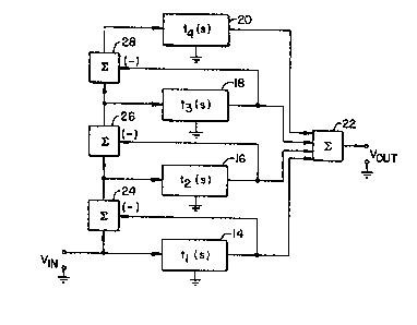
Figure 3 illustrates the equivalent arrangement
described in the summary of the invention. Four three-
terminal elements 14, 16l 18 and 20 are shown having
transfer functions tl(s)! t2(s), t3(s), and t4(s),
respectively. Each element has its second terminal
connected to ground and has its third terminal output
connected to a summing means 22. The input signal V
is applied to the first terminal of element 14 with
respect to ground and to a first summing meAns 24. The
input to element 16 is the output of element 14
subtracted by summing means 24 from the input Vi . The
input to element 18 is the output of element 16
subtracted by summing means 26 from the input to
element 16. The input to element 20 is the output of
element 18 subtracted by summing means 28 from the
input to element 18.
Figure 4, also referred to in the summary of the
invention, illustrates more generally the preferred
~2~7~
-34-
embodiment discussed in connection with Figure 8. In
the arrangement of Figure 4 four three-terminal
elements 30, 32, 34, and 36 are shown having transfer
functions t1(s), t2(s), t3(s), and t4(s), respectively.
The input signal Vi is applied to the first terminal
of elements 30, 32, 34, and 36 with respect to the
reference potential (shown as ground). Only the second
terminal of element 30 is connected to a reference
potential. The input to the second terminal of element
32 is the output of element 30 (from its third
terminal). The input to the second terminal of element
34 is the output of element 32 (from its third
terminal). The input to the second terminal of element
36 is the output of element ~ (from its third
terminal). The overall output is taken between the
third terminal of element 36 and the reference
potential. This general arrangement can be described
as "stacking" of elements and is believed to be the
simplest and most effective way in which to implement
the invention.
Figure 5, the transition between the arrangements
of Figures 3 and 4 referred to in the summary of the
invention, illustrates another possible circuit
topology that :is equivalent. Four elements are used
solely for the purposes of illustration in Figures 3,
4, and 5. Superposition effects in accordance with the
teachings of this invention can be achieved using two
or more elements, at least one being dynamic, as is
explained further below. In the arrangement of Figure
5 four three-terminal elements 38, 40, 42, and 44 are
shown having transfer functions tl(s), t2(s), t3~s),
and t4(s), respectively. The input si~nal Vi is
~z~
-35-
apylied to the first terminal of elements 38, 40, 42,
and 44 with respect to the reference potential lshown
as ground). Only the second terminal of element 38 is
connected to the reference potential. The input to the
second terminal of element 40 is the output of element
38 (from its third terminal). The input to the second
terminal of element 42 is the summation (from summing
means 46) of the output of element 38 and the the
output of element 38 subtracted from the output of
element 40 (derived in summing means 48). The input to
the second terminal of element 44 is the summation
(from summing means 50) of the output of summing means
46 and the output of summing means 46 subtracted from
the output of element 42 (derived in summing means 52).
The overall output is taken from summming means 54
which combines the output from element 38, summing
means 48, summing means 52, and summing means 56, which
subtracts the output of summing means 50 from the
output of element 44.
The stacking arrangement of Figure 4 can be
further modified by introduciny branching such as shown
in Figure 10. Such arrangements may be useful in
creating more complex superposition effects than are
possible with a direct or straight linkage such as in
Figure 4. In the Figure l0 modification the second
"level" in the stack has two elements rather than one.
Thus, the input Vi is applied to the first terminal of
blocks 58, 60, 62 and 66 having respective transfer
functions tl(s), t2(s), t3(s) and t4(s). The second
terminal of the three-terminal network of block 58 is
connected to a reference potential ~e.g., ground) and
its third terminal feeds the second terminals of blocks
~27135;~6
-36-
60 and 62. The outputs from the third terminals of
blocks 60 and 62 are added in summing means 64 and
applied to the second terminal of block 66. The
overall output is taken from the third terminal of
block 66. Other branching arrangements are possible:
the arrangement of Figure 10 is only one example of the
manner in which elements may be configured in
accordance with the invention.
Although not shown in Figures 3, 4, 5, and lQ, the
linkages between elements may be buffered or
unbuffered, but preferably are buffered, as discussed
above. In addition, while the general arrangements
thus far shown employ three-terminal networks,
equivalent circuit arrangements are possible based on
these teachings in which some or all of the elements
are three or four terminal networks each of which
"floats" or is connected to a reference potential. For
example, transformers and various isolation techniques
could be employed to achieve the basic "differential
feed, summed output" arrangement inherent in Figures 3
through 5 and 8 through 10.
With respect to any combination of elements in
accordance with the teachings of the invention, in
order to provide an overall compressor or expander
action, at least one element must have a transfer
function that is a compressor or expander function.
All of the elements which are active (e.g., have
characteristics that vary dynamically in response to
signal conditions) generally must act in the same sense
(e.g., provide compressor or expander action). One or
more elements may have a passive characteristic (e.g.,
~2~ G
-37-
the characteristic does not vary dynamically in
response to signal conditions). It may be useful to
have more than one passive element provided that the
active element has a dynamic characteristic such that
as it varies different aspects of the passive
characteristics are revealed.
Although arrangements of elements in accordance
with the invention can function as stand alone
compressors and expanders, it is preferred to e~ploy
them in one or more side paths of dual path compressor
and expander arrangements of the type generally
described in US-PS 3,846,719, US-PS 3,903,485, US-PS
4,490,691; and US-PS Re 28,426.
Active elements each preferably have their
variable conditions controlled by their own control
circuits, although for certain purposes it may be
acceptable to control more than one active element with
a single control circuit. hhere individual control
circuits are employed, although it is possible for
these control circuits to operate independently only in
response to the signals in each element, in practice
the overall circuit performance may be impeoved by
applying additional signals to the control ciecuits, as
described further below. It will be apparent that the
simple analysis based on steady-state attenuator
elements may not fully apply in practice under dynamic
conditions where the elements have control circuits and
where those control circuits can have interconnections
to other elements and portions of the overall system
environment.
~:7~
~38-
It will also be appreciated that some active
elements may have thresholds at which dynamic action
will begin in response to a dominant signal. In
designing a stack of elements, the selection of
different threshold levels among the active elements
may be advantageous so as to influence the sequence in
which the characteristics of the various elements
emerge in response to various dominant signal
conditions. In general, however, in order to achieve
superposition effects, the active or dynamic elements
must be active in generally the same level range. That
is, the range of input signal levels that cause dynamic
action should be substantially the same, subject to
variations of a few decibels.
The arrangement of Figure 11 is useful in
illustrating the way in which multiple elements with
various characteristics may be usefully combined and in
describing the setting of relative thresholds arnong
elements in a stack. For simplicity and ease of
understanding only the principal components necessary
to illustrate the concept are shown in this Figure (and
the Eollowing Figures 13 through 16). The arrangernent
may form the noise reduction side path in a dual path
compressor or expander or, alternatively, it may form a
stand alone compressor. This arrangement is but one
example of the way in which multiple elements with
different characteristics can be combined. Another
useful combination of elements is to provide for
elements with upward acting and downward acting sliding
band characteristics within the same frequency band.
~7~3526
~39-
A five element stack is sho~n in Figure 11 having
a wideband attenuator element 68, a fixed band
attenuator element 70, a sliding band element 72, a
first spot frequency attenuator element 74 and a second
spot frequency attenuator element 76. Each element
receives the input signal. High pass filters 78 and
80f each having an 800 Hz corner frequency, form a part
of the transfer functions of elements 70 and 72. Band
pass filters 82 and 84, centered at 960 Hz (an audio
interference frequency related to head rotation in
quadruplex videotape recorders) and at 15.75 kHz (an
audio interference frequency at the horizontal sweep
frequency in 525 line television systemsJ form a part
of the transfer functions of elements 74 and 76,
respectively. Each element has its own independent
control circuit 86, 88, 90, 92, and 94, essentially a
rectifier and smoothing circuit including an amplifier
which can have frequency weighted or wideband gain, as
may be necessary. Preferably, each control circuit
responds only to the output of its respective element;
that is, the control signal is derived differentially
using combining means 89, g1, 93, and 95 (note
subtractive feed from bottom of each element). The
control circuits control the variable resistance
elements 96, 98, 100, 102, and 10~, which, in practice
may be FETs, the control voltage being applied applied
to their gate input. The fixed band attenuator
elements 68, 70, 74 and 76 have series resistors (106,
108, 110, and 112, respectively) to form a variable
voltage divider in conjunction with the FETs. The
sliding band element 72 has a series capacitor 114 to
form a variable high pass filter in conjunction with
the FET. In the manner of the preferred stack
-40-
arrangement of Figure 4, element 68 is driven with
respect to a reference, shown as ground and each of the
other elements is driven through a buffer (unity gain
buffers 116, 118, 120, and 122) with respect to the
output of the element below it. Note that each filter,
if included, also has its reference terminal connected
to the output of the element below it. Each element
has a threshold level such that when the signal level
rises in the element and reaches that level a change in
the variable element begins. ~ach element is assumed
to provide a maximum of 10 dB of dynamic action. The
overall output of the arrangement is from the output of
the top element through a unity gain buffer 124.
In the quiescent state, the defining envelope of
the arrangement of Figure 11 is a total dynamic action
of 10 dB, wideband. As signal components appear, the
characteristics of the various elements emerge in
response to the frequencies and levels of the
components. ~he sequence in which the characteristics
of elements emerge in response to those signal
components will depend on the operating frequency range
of the respective elements and their relative threshold
levels.
Consider first two examples. If a 200 Hz tone
appears, starting at a sub-threshold level and
gradually rising in level, the wideband element is
eventually defeated, but the others remain fully
effective. Thus the overall characteristic, shown in
Figure 12A, is that of the 800 Hz fixed and sliding
bands, which are coincident and partly hide the two
spot frequency characteristics: the tip of the 960 Hz
i2~
-41-
spot frequency characteristic and the sliding band
characteristic, the high pass filter of the sliding
band having moved upwardly in response to the 2 kHz
tone. The sliding band characteristic hides the 15.75
kHz spot frequency characteristic~
In the arrangement of Figure 11, each element has
its own control circuit which operates entirely in
response to signals within the respective element as a
result of the differential derivation of the control
signals. Elements may have each have a totally
independent control circuit, with or without
differential derivation, and various cross connections
are possible. The cross connections illustrated in
Figures 13 and 14 are useful in permitting different
thresholds to be set in the elements while retaining
adequate control circuit gain in the sliding band
element at frequency extremes. Another type of cross
connection, referred to as "parking" is described below
in connection with Figures 16A and 16B.
Referring to Figure 13, a fixed band element 126,
a wideband attenuator, is shown stacked with a sliding
band element 128, a sliding shelf acting upwardly in
frequency and having a wideband quiescent character-
istic: substitution of an inductive element instead of
the capacitor would result in a sliding shelf acting
downwardly in frequency. As a practical matter, a
gyrator circuit would be used to simulate an inductor.
The fixed band element has a series resistor 130 and a
shunt FET 132, connected to a reference potential,
which form a variable attenuator as the resistance of
the source-drain path of the FET is controlled in
i2~
-42-
response to a control voltage applied to its gate. The -
output of the fixed band element is applied through a
buffer amplifier 134 to a rectifier and smoothing
circuit 136. The sliding band element 128 includes
parallel capacitor 138 and resistor 140 shunted by FET
142 which is connected to the output of the fixed band
element, at the output of buffer 134. The output of
the sliding band element is applied to a buffer
amplifier 144, an optional combining means 150, and a
rectifier and smoothing circuit 146 which provides a
control voltage to the FET 142. The output of the
combination of elements is taken from buffer amplifier
144.
As noted in connection with the arrangement of
Figure 11, it is possible to use the output of one
element in a stack to buck the output of the next
element in generating the control voltage of that next
element. This is shown not only in Figure 11 but also
in Figure 13 where the output of the sliding band
element from buffer 134 is subtracted from the output
of the fixed band element from buffer 144 in the
combining means 150. The bucking signal ~rom the fixed
band element can be treated so as to be more or less
than the sliding band element output (by amplification
or attenuation) and the sense of the bucking signal can
be inverted so that as the fixed band element output
increases the bucking signal decreases. These
principles apply generally to successive active
elements in any arrangement according to the invention.
A further alternative is shown in Figure 14 in
which the bucking signal from the fixed band element is
7~
-43-
first conditioned by a filter 152 located in the
control circuit loop for the fixed band element.
Typically~ the filter would be a high pass or low pass
filter located within the operating band of the overall
circuit. An unfiltered bucking signal, shown as a
dashed line, may simultaneously be applied in the
manner of the alternative version of Figure 13 (e.g.,
with optional combining means 150). The filtered
bucking signal can be treated as mentioned in
connection with the unfiltered bucking signal of Figure
13.
In a further control circuit coupling variation,
it is possible to feed the rectified signal in the
control circuit of one element into the DC portion of
the control circuit of another element. For example,
in Figure 13, the summing means 150 would be located
between the output of rectifier and smoothing circuit
146 and the gate of FET 142, and the bucking signal
from element 126 would be taken from the output of
rectifier and smoothing circuit 136. This alternative
is advantageous where the signal phase relations may
not be correct for AC combining/bucking as in the
method discussed above. However, a disadvantage is
that it is not possible to apply selective filtering of
the coupled component, as in Figure 14.
In some applications it may be possible to
eliminate one control circuit and use a common control
circuit for two elements as is shown in Figure 15,
although the use of individual control circuits for
each element is preferred to produce a more conformal
effect. (The same reference numerals are used for
1~7~352~
-44-
common components in Figures 13 through 15.) In Figure
15, the output of the fixed band control circuit from
the rectifier and smoothing circuit 136 is applied
through a buffer 148 in order also to control the
sliding band FET 142.
Figure 16A shows a modification of Figure 14 in
which an additional feature referred to as "parking" is
incorporated in the circuit. The concept of parking is
based on the observation that it is often advantageous
to pre-set or "park" a response characteristic at some
level and/or frequency other than its quiescent level
and/or frequency when the element is below its
threshold. In the case of the fixed band element, the
fixed band control circuit is parked at a level just
below its threshold so that the circuit reacts more
quickly in response to changes in the input signal. A
detector 153 senses the fixed band control signal,
develops an appropriate signal and applies it to
summing means 155 where it is added to, or takes over
from, the control signal to provide the fixed band
parking signal. In operation, the parking signal level
preferably is set just below the fixed band threshold.
Above the threshold, the fixed band control circuit
takes over to the exclusion of the parking detector.
Thus, the detector 153 is required to sense the fixed
band control signal and to provide, only when the fixed
band element is below its threshold, the correct signal
level for parking the fixed band control circuit at the
desired level. A detector providing these functions
may be implemented in various ways: one suitable
arrangement is to sense the fixed band control voltage
with a "perfect diode" circuit. Such circuits are well
78526
27332-34
known and employ an operational amplifier biased so that the
circuit switches its output from positive to negative when the
signal being sensed rises to the bias voltage. The perfect
diode circuit output, suitably adjusted in level as may be
necessary, acts as a maximum selector circuit which takes over
from the fixed band control signal to provide the desired parking
signal.
Figure 16B shows generally another arrangement of
stacked fixed band and sliding band elements employing parkiny.
In this case the sliding band element 129 has and inductor 139
(simulated by a gyrator circuit in practical embodiments) so
that the sliding band circuit operates downwardly. In the
arrangement of Figure 16s, parking is provided not only in the
fixed band circuit but also in the sliding band circuit. As
applied to the sliding band circuit, the concept of parking is
based on the observation that as long as the fixed band umbrella
characteristic is present, then it is possible to pre-slide
the sliding band ("park" it) to the frequency region where the
action is likely to be when a signal is applied. This improves
response time and reduces modulation distortion. In its
quiescent state the downwardIy acting sliding band would normally
be in its wideband state (in the absence of any parking circuit)--
that is, the high frequency cutoff would be infinity, i.e., well
into the low frequency stop-band if the circuit were employed in
an arrangement such as described below in connection with
Figure 19. Referring again to Figure 16B, when a signal appears
-45-
~ 5~6 27332-34
the band slides down to attenuate the dominant signal, which
with speech and music very likely will be in the range 100 Hz -
1 kHz. Therefore, it is useful to park the low frequency
sliding band at a cutoff frequency of about 400 Hz, just into
the low frequency pass-band of the Figure 19 arrangement.
Referring again to Figure 16B, the parking influence is
remGved as soon as the signal rises above the fixed band threshold
as this marks the imminent reduction or disappearance of the fixed
band umbrella. Detector 153 senses the fixed band control signal
in relation to a reference voltage and develops the parking
signal wh`ich is applied to the sliding band FET 142 via combining
means/maximum selector 151. After the signal has risen above
the fixed band threshold, if the applied frequency is lower
than 400 Hz, the sliding band control circuit takes over and
slides the band down further. If the frequency is above 400 Hz,
the sliding band control circuit still takes over but allows the
cutoff frequency to slide up. The detector 153 is required to
sense the fixed band control signal and to provide, only when
the fixed band element is below its threshold, the correct signal
level for parking the sliding band circuit at the desired
frequency. The detector described in connection with the
arrangement of Figure 16A is also suitable for the arrangement
of Figure 16B.
While sliding band parking arrangements can be used in
connection with high frequency sliding band circuits as well, the
advantages are less because the likely applied signal frequencies
-46-
~27~3S~
27332-34
are in the high frequency stop band frequency range (referring
to arrangements such as in Figuresl9 and 20), which is already
the right way around, in contrast with the low frequency
situation.
-46a-
3l2~1~5~
-47-
Figure 16B shows an additional feature, related to
the parking circuits described above, for reducing
noise generated by the gyrator simulated inductance
139. A shunt shown as switch 157 is connected across
the inductor 139. The switch is controlled by the
signal from detector 153. Eelow the thresholds of the
fixed band and sliding band circuits, as sensed by
detector 153, there is no need for the sliding band
circuit 129 and the inductor 139 to be active. Thus,
the gyrator simulated inductance is shorted out by the
shunt when the circuits are below their threshold. In
a practical circuit, the shunt can be implemented using
an FET, the signal from detector 153 being applied to
the FET gate. Alternatively, the shunt could be
located across any input point to an appropriate output
point, the two points having the same signal levels.
The use of a shunt to eliminate noise in an active
element could be used in any bi-linear or uni-linear
compressor or expander circuits because in such
circuits there is a range of input signal levels in
which the circuit provides no dynamic action. Such a
shunt is not necessarily related to parking circuits.
In the arrangement of Figure 16B the parking signal
derived from detector 153 merely happens to be suitable
for control of the shunt.
The parking and the gyrator shunt features of the
embodiments of Figures 16A and 16B need not be employed
in the context of the Figure 14 arrangement. For
example, the use of a filter 152 is not essential. The
parking feature could be applied to a general
arrangement such as that of Figure 11.
~æ~,
-48-
The cross coupling arrangements of Figures 13
through 16B thus provide considerable flexibility for
the circuit designer in determining the manner in which
the thresholds of the two elements will interact.
In principle, where the stacked elements each have
separate and independent control circuits with full
differential control, such as in the arrangement of
Figure 13, the order of the elements in the stack is
immaterial: the same results should be obtained with
the elements arranged in any order. However, where
there is no cross coupling in the control circuitry, or
a cross coupling that provides only a partial
differential control (as in Figure 14 when the only
bucking signal is from filter 152J, the order in which
the elements are stacked may affect the overall result.
In order to understand the operation of a two
element stack made up of fixed band and sliding band
elements (such as in Figures 13 through 16), assume
that a fixed single pole high pass filter with a corner
frequency of 800 Hz, for example, is placed in series
to the inputs to the two elements and that the
effective threshold of the fixed band element is -62 dB
and that of the sliding band element is -66 dB. Each
element is assumed to provide a maximum of 10 dB of
attenuation. If, for example, a 12 kHz signal is
applied at a level of -66 dB, the corner frequency of
the sliding band characteristic begins to slide but
nothing happens to the overall characteristic envelope
because the fixed band is still inactive and supports
the envelope. The altered sliding band characteristic
is hidden. This situation, shown in Figure 17A, which
~7~ 6
-49-
has the same envelope as the quiescent condition, but
showing the altered sliding band characteristic in
phantom, continues until the signal reaches the -62 dB
threshold of the fixed band element. As the signal
rises above the fixed band threshold (by a few dB), the
fixed band begins to attenuate revealing the top of the
sliding band characteristic, which continues to slide
upward as the siynal level rises. This situation is
shown in Figure 17B. As the signal level increases
several more dB above the fixed band threshold, the
fixed band continues to attenuate and the sliding band
continues to move upward as shown in Figure 17C.
As discussed in US-PS ~e 28,426, in order to
obtain full attenuation of the sliding band FET, it is
necessary to have a sufficiently high gain in the
control signal loop at high levels. The solution set
forth in that patent is to provide high frequency
weighted amplification in the loop. However, a
drawback to that approach is that the loop gain is too
high at lower levels (thus causing the band to slide
farther than necessaey) and it is also difficult to
maintain a sufficiently high sliding band threshold.
By employing the cross coupling techniques
described in connection with Figures 13 and 14 it is
possible to achieve the desired sliding band threshold
with the desired loop gains at high and low signal
level conditions. If the arrangement of Figure 13 with
the optional combining means 150 is used (i.e., full
bucking effect), then below the fixed band threshold
there would be no control signal drive at all to the
sliding band FET and under very high level conditions
-50-
when the fixed band is defeated (e.g., full
attenuation), no further bucking is provided and full
gain is provided in the sliding band contzol signal
loop.
In practice, the full bucking approach provides
more bucking effect than is necessary and improved
performance is achieved if the bucking action is
allowed to be less. For example, the effective high
frequency gain of the sliding band control signal loop
may be reduced by about 5 dB as long as the fixed band
is not attenuated and then as it attenuates the bucking
action is decreased until it reaches 0 dB when the
fixed band is fully attenuated. In critical
applications, where a high sliding band threshold is
desired, the arrangement of Figure :L4 allows the use of
both wideband and frequency selective bucking action.
In the case of a high frequency sliding band element,
the frequency selective bucking signal is derived using
a high pass filter (filter 152, Figure 14) since the
bucking action is most desirable at the high frequency
extreme, where the equalized control amplifier provides
the highest gain. In one practical embodiment
described further below a cutoff frequency of 1.6 kHz
is employed. E'or a low frequency sliding band element,
the requirement is to provide high loop gain at high
level low frequencies. In that case, the filter 152 in
the arrangement of Figure 14 is a low pass filter. In
one practical embodiment described further below a
cutoff frequency of 400 Hz is employed.
As mentioned above, a very useful arrangement is
to provide a compressor or expander configured in the
-51-
nature of bandsplitting high frequency and low
frequency stages, each stage made up of sliding band
and fixed band elements. The parallel stages can
operate as stand alone dynamic range modification
devices or as side paths in Type I or Type II dual path
arrangements such as described in US-PS 3,846,719; US-
PS 3,903,485; US-PS Re 28,426; and US-PS 4,490,691.
Preferably, single pole filters with the same corner
frequency in each are employed so that the cornbined
quiescent response of the two stages is flat. An
advantageous corner frequency for the high and low
frequency stages is about 800 Hz for an audio system.
With the gently sloping 6 dB/octave slope of the
filters, if the high frequency stage has a corner
frequency of 800 Hz, the stage provides significant
action as low as 100 or 200 Hz. If the low frequency
stage also has a corner frequency of 800 Hz, it
provides significant action as high as 3 kHz to 6 kHz.
Thus, for signals lying in the range of, say 100 Hz to
~ kHz, which is the band having most of the energy in
typical music, both stages are effective and provide a
signal tracking effect. For example, as explained
further below, for a single dominant signal in that
ranye, the overall response is that of two sliding
bands, above and below the dominant signal. For more
than one dominant signal the resulting characteristic
is a fixed band response between the most upper and
most lower dominant signals and sliding band responses
above and below the most upper and most lower dominant
signals, respectively.
In Figure 18, an embodiment of a high frequency
stage is shown. A single pole high pass filter 154
521~
-52-
with a cutoff frequency of 800 Hz is located in its
input. In practice the filter includes an operational
amplifier so as to buffer the filter from the following
circuitry. The high pass filtered input signal is
applied tc a fixed band element 156 and to a sliding
band element 158. The fixed band element includes an
input resistor 160, a shunt FET 162 operated as a
variable resistor, and a control circuit 164 that
generates a DC control signal which is applied to the
gate of the FET 162. The FET resistance drops as the
DC control signal level increases. ~ixed band control
circuit 164 includes in its loop a buffer amplifier
166, a single pole high pass filter 168 having about a
400 Hz cutoff frequency, a rectifier 172 (preferably
full-wave), and a smoothing circuit 174 (which also is
employed to adjust the attack and release time
constants of the control loop~. The sliding band
element 158 includes parallel input resistor 178 and
capacitor 180 which are shunted by FET 182. The
sliding band element has a control circuit 184 which
includes a buffer amplifier 186, a summing means 188, a
high frequency emphasis circuit 190, a rectifier 192
(preferably full-wave), and a smoothing circuit 194.
The summing circuit also receives as inputs bucking
signals taken before and after a high pass filter 170
having about a 1.6 kHz cutoff frequency. The bucking
signals are suitably buffered to avoid undesired
interaction between the control circuits. The input to
filter 170 is taken between filter 168 and rectifier
30 172. The output of the fixed band element 156 is
applied to the sliding band element through buffer 198.
The overall output is taken from buffer 186 of the
sliding band element 158.
~;271~2~
-53-
In operation, the stacked fixed band and sliding
band elements operate generally in the manner described
above. The coupling of bucking signal components from
the fixed band element to the control circuit of the
sliding band element are for the reasons set forth in
connection with the description of Figure 14, a~ove. A
corner frequency of about 1.6 kHz was chosen for filter
170 because differential control of the sliding band is
needed only at high frequencies. Filter 168 is
employed in order to reduce the sensitivity of the
fixed band circuit to very low frequency components.
In Figure 19, an embodiment of a low frequency
stage is shown. The input signal is applied to a fixed
band element 200 and to a sliding band element 202.
The fixed band element includes an input resistor 204,
a shunt FET 206 operated as a variable resistor, and a
control circuit 208 that generates a DC control signal
which is applied to the gate of the FET 206. The FET
resistance drops as the DC control signal level
increases. Control circuit 208 includes in its loop a
buffer amplifier 210, a first single pole low pass
filter 212 having a corner frequency of about 800 Hz, a
second low pass filter 214 having a corner frequency of
about 1.6 kHz, a rectifier 218 (preferably full-wave),
and a smoothing circuit 220 (which also is employed to
adjust the attack and release time constants of the
control loop).
The sliding band element 202 includes parallel
input resistor 224 and inductor 226 which are shunted
by FET 228. In practice, the inductor 226 is simulated
by a gyrator circuit which includes operational
7~ 6
-54-
amplifiers (such circuits are well known and is not
shown). The sliding band element has a control circuit
230 which includes a buffer amplifier 232, a single
pole low pass filter 234 having a corner frequency of
about 800 Hz, a summing circuit 236, a low frequency
emphasis circuit 238, a rectifier 240 (preferably full-
wave), and a smoothing circuit 242. Low pass filter
234 is preferably located in the position shown in
order to assist in suppressing undesired noise
generated in the low frequency stage. Alternatively,
the filter may be located in the input to the
arrangement as is done in the high frequency circuit of
Figure 18. The summing circuit 236 also receives as
inputs bucking signals taken before and after a low
pass filter 216 having a corner frequency of about 400
Hz. The bucking signals are suitably buffered to avoid
undesired interaction between the control circuits.
The input to filter 216 is taken between filter 214 and
rectifier 218. The output of the fixed band element
200 is applied to the sliding band element through
buffer ~. The overall output is taken from filter
234 of the sliding band element 202.
In operation, the low frequency stacked fixed band
and sliding band elements operate generally in the
manner described above except that the sliding band
elelnent operates downwardly in frequency. One
difference in the low frequency stage, as noted above,
is that the band defining filter is located in the
stage output rather than in the input as in the high
frequency stage~ The coupling of bucking signal
components from the fixed band element to the control
circuit of the sliding band element are for the reasons
~l~7~6
-55-
set forth in connection with the description of Figure
14, above. A corner frequency of about 400 Hz was
chosen for filter 216 because differential control of
the sliding band is needed only at low frequencies.
Filters 212 and 214 are employed in order to reduce the
sensitivity of the fixed band circuit to very high
frequency components.
High frequency and low frequency stages of the
type set ~orth in Figures 18 and 19 can be used as
building blocks in creating eompressors, expanders and
noise reduction eompanders. For example, high
frequency and low frequency stages of the type
described in Figures 18 and 19 may be employed as side
paths in dual path arrangements in the manner shown in
Figures 20 and 21.
In Figure 20 a Type I dual path arrangement (of
the type generally described in US-PS 3,846,719) is
shown having a compressor 248 in which the input signal
is applied to the high frequency stage 250, to the low
frequency stage 252 and to the main path 254. The
outputs of stages 250 and 252 are summed in summing
means 256 and l:hen sumnled with the main path signal
eomponents in summing means 258 to provide the
eompressor output for applieation to a transmission
ehannel. The side path signal eomponents thus boost
the main path signal eomponents eausing eompressor
aetion. The transmission channel output is applied to
the expander 260, configured in a complementary manner
to the compressor 248, which has an input summing means
262 which receives the transmission channel output and
~78S26
27332-34
subtracts the sum of the high frequency stage 250 and low
frequency stage 252 ou-tputs, which are added in summing means
263. The main path 264 receives the output of summing means
262 and couples the signal components from that means to the
output and to the inputs of stages 250 and 252. The side path
signal components thus buck the main path signal components caus-
ing expander action.
In Figure 21 a Type II dual path arrangement (of
the type generally described in US-PS 3,903,485) is shown having
a compressor 268 which has an input summing means 270 receiving
the input signal and the sum of the high frequency stage 250
and low frequency stage 252 outputs, which are combined in
summing means 272. The summing means 272 has its output
applied to the main path 274 which provides the compressor
output to the transmission channel and the input to the stages
250 and 252 of the compressor. The side path signal components
thus boost the main path signal components causing compressor
action. The transmission channel output is applied to the
expander 276, configured in a complementary mannèr to the
compressor 268. The input signal is applied to the high
frequency stage 250, to the low frequency stage 252 and to the
main path 278. The outputs of stages 250 and 252 are summed
in summing means 280 and then subtracted from the main path
signal components in summing means 282 to provide the expander
output. The side path signal components thus buck the main
path signal components causing expander action.
-56-
. ~
1~78~2~ 27332-34
In Figures 20 and 21 the main path of each compressor
and expander is linear with respect to dynamic range and the
level of the sum of the side path high frequency and low
frequency stages is less than the maximum level of the main
path. The transmission
-56a-
~7~5~i
57
channel in those Figures and in Figures 22 and 23,
below, may include any type of storage or transmission
medium and may also include means for converting or
encoding the analog sighal components from the
compressor into a different form (digital, for
example), the storage or transmission of the encoded
signals, and means for re-converting or decoding the
encoded signals back into analog signal components.
In arrangements such as in Figures 20 and 21 where
only one high frequency stage and one low frequency
stage is used in each compressor and expander it is
practical to provide a maximum of about 10 to 12 dB of
noise reduction without reaching excessive maximum
compression or expansion ratios. Although the
arrangements of Figures 20 and 21 will be adequate in
certain applications, it is useful to employ the
teachings of US-PS 4,490,691 to achieve a greater
amount of overall noise reduction without placiny an
undue burden on any one stage or creating excessive
compression or expansion ratios.
In Figure 22 one possible arranyement is shown in
which there are three series Type I dual path stages in
the compressor and three complementary stages in the
expander. The threshold levels of the series bi-linear
circuits are staggered, employing the staggering
aspects of US-PS 4,490,691. Alternatively, a Type II
configuration could be employed. The embodiment of
Figure 22 also employs the spectral skewing and
antisaturation aspects of US-PS 4,490,691, although
these aspects are not essential to a multi-stage
arrangement employing high frequency and low frequency
stages.
-~:27~6
58
The compressor portion of the system of Figure 22
has three stages: a high level stage 284, which has
the highest threshold level; a mid-leveL stage 286; and
a low level stage 288, which has the lowest threshold
level. As discussed in US-PS 4,490,691 this is the
preferred order of arrangement of staggered stages,
although the reverse order is possible. The expander
portion of the system of Figure 22 also has three
stages arranged complementary to the compressor: the
low level stage 290, the mid-level stage 292, and the
high level stage 294. Each high level and mid-level
stage has both a high frequency stage 250 and a low
frequency stage 252. The low level stage has only a
high frequency stage 250 and no low frequency stage.
Each high frequency stage 250 and each low frequency
stage 252 is of the type described in connection with
Figures 18 and 19. In practical circuits there may be
some diffeeences between or among high frequency and
low frequency stages depending on whether it is located
in the high level, mid-level or low level stage.
If each compressor stage (284, 286, 288) and each
expander stage (290, 292, 292) has, for example, 8 dB
of compression or expansion, respectively, then the
overall compander system will provide 24 dB of noise
reduction in the high frequency band (above 800 ~z, if
the high frequency stages have an 800 Hz cutoff
frequency) and 16 dB of noise reduction in the low
frequency band (below 800 Hz, if the low frequency
stages have an 800 Hz cutoff frequency). Such an
arrangement is useful, for example, in a high quality
audio noise reduction system of the type used in
professional applications.
~2~ 2~
59
The cascading of staggered stages as in the
embodiment of Figure 22 is useful not only to increase
the amount of compression and expansion but also to
create a ~uasi-multi-pole effect (with respect to the
band of the high frequency stages) and a quasi-two-pole
effect (with respect to the band of the low frequency
stages). Thus, while each circuit itself has only a
single pole band determining filter, in order to allow
for broad frequency overlap of the circuits and a flat
overall frequency response when the bands are combined,
the overall effect when two or three circuits are
cascaded is to provide a steepness compounding or stage
ganging effect: in effect, a two or three pole filter.
The additional sharpness of a two or three pole filter
is desirable in that it allows the system to track
dominant signal components more effectively. That is,
with steep filter slopes, frequencies adjacent to a
dominant signal con,ponent are affected as little as
possible by dynamic action. The quasi-two-pole and
three-pole filter effect brings about that result while
retaininy the advantages of single pole filters in each
individual circuit, namely that the outputs of the high
and low frequency circuits combine perfectly in both
amplitude and phase. The overall result is that the
filter action becomes more complex as signals are
applied by virtue of the multi-stage steepness
compounding effect taken in combination with the quasi-
two-pole filter effect in the noise reduction side
paths of each circuit. The latter effect results from
the use of a single pole fixeâ filter in series with a
variable shelf characteristic in the sliding band
portion of the circuits which has a single pole
characteristlc in its quiescent condition but which
~2~8526
tends toward a two-pole characteristic in the presence
of a dominant signal or signals. The intervention of
the fixed bands, via action substitution, further
tailors the response.
The input to the compressor portion of the system
is applied to low frequency and high frequency spectral
skewing networks shown as block 296. In a practical
embodiment there are two networks in series: a two
section low frequency network made up of a 50 ~z high
pass single pole shelving section and a 2Ct Hz high pass
single pole filter section; and a 12 kE~z Eutterworth
(maximally flat) low pass filter network. Both
networks may be implemented using well known
operational amplifier active filter techniques.
Complementary de-skewing networks are located in block
304 at the output of the expander.
The n,ain path of each stage 284, 286, and 288 in
the compressor portion includes low frequency and high
frequency antisaturation networks 298, 300, and 302,
respectively. Complementary antisaturation networks
304, 306, and tO8 are located in the main path of each
stage 290, 292, and 294, respectively, in the expander
portion. As discussed in US-PS 4,490,691, it is
possible to locate such networks in the main path of
only one stage in the compressor and in the
complementary location in one stage in the expander
portion of a series of cascaded staggered stages.
The Type I stages of Figure 22 also include
summing means 310, 312, 314 and 316 that combine the
outputs of the high frequency and low frequency
~z~S~6
~1
circuits in stages 284, 286, 292, and 294l
respectively. The stages each include summing means
318, 320, 322, 324, 326, and 328 in the main paths
which couple to the main path the side path output, in
the case of stages 288 and 290, or the outputs of the
side paths, in the case of the other stages.
The arrangement of Figure 22 is only one example
of compressor, expander or compander systems that can
be constructed using the high frequency circuits and/or
the low frequency circuits of the type described in
connection with Figures 18 and 19. Other possibilities
include, but are not limited to, (1) a single high
frequency circuit in the compressor and expander; (2)
one high frequency circuit and one low frequency
circuit each in the compressor and expander (as in the
examples of Figures 20 and 21); and (3) two high
frequency circuits and one low frequency circuit each
in the compressor and expander (e.g., an arrangement
such as in Figure 22, but omitting the high level
stages 284 and 294). Alternative (1) would provide a
degree of compatibility with widely used B-type
consumer noise reduction systems licensed by Dolby
Laboratories and alternative (3) would provide a degree
of compatibility with the widely used A-type
professional noise reduction systems manufactured by
Dolby Laboratories. Other configurations are possible
depending on the goals of the system designer. For
example, a fourth stage could be added to the
compressor and expander portions of the example of
Figure 22 and/or the low level stage of that example
could additionally include a low frequency circuit.
62
In a practical embodiment of a system generally in
accordance with the example of Figure 22 it is possible
to employ only one set of high level, mid-level and low
level stages by using a unique circuit and switching
arrangement. Figure 23 is a block diagram of such a
practical embodiment. The circuit and switching
arrangement is applicable to all types of compander
systems having series dual path stages in which
simultaneous encoding and decoding is not required. A
single pole double throw switch provides switching of
the system from its compression mode to its expansion
mode. In order to provide this simplicity in
switching, the arrangement employs a supplemental main
path in each stage except the last.
Referriny to Figure 23, the input to the system is
through a bandpass filter 330 which is intended to
remove subsonic and supersonic signals (for example,
the filter may be comprised of a two pole high pass
filter with about a 10 Hz cutoff frequency and a two
pole low pass filter with about a 50 kHz cutoff
frequency). The filtered input signal passes through
first and second inverting buffer amplifiers 332 and
334 (configured as summing operational amplifiers with
appropriate resistors 332a, 332b, 332c, 334a, 334b, and
334c) to the system output. The main path of the
system is between amplifiers 332 and 334. At a point
between buffers 332 and 334 the input to three paths is
derived; the three paths include a first path 336
including a low frequency and high frequency spectral
skewing network 338 feeding three stages (340, 342,
344), the first two (340, 342) having supplemental main
paths (346, 348), a second path 350 which includes a
~278S26
27332-34
low frequency and high frequency antisaturation network 352 and
generates an antisaturation bucking signal, and a gain trimming
path 354. The effect of network 352 is to create sir~lilar
characteristics described in connection with network 296 of
Figure 22. The effect of network 352 is to create similar
characteristics as networks 298, 300, and 302 of Figure 22,
but further includes amplification means as may be necessary to
generate a bucking signal of the proper level and polarity.
Signal components from the three paths are combined in summing
means 356, the output of which is applied to the switching
arrangement 358. That is, network 352 has a low frequency and a
high frequency boost characteristic so that when the signal is
combined in a bucking sense the overall low frequency and high
frequency antisaturation characteristics are obtained.
The first stage 340 is preferably the high level
stage which includes a high frequency circuit 250 and a low
frequency circuit 252, as in Figure 22. The input to stage
340 is fed to circuits 250, 252 and the secondary main path 346.
The output of each (e.g., 250, 252, 346) are combined in summing
means 364. The second stage 342, the mid-level stage, receives
the output of summing means 364 and applies that to further
high frequency and low frequency stages, 250 and 252, respectively,
and to secondary main path 348. The output of circuits 250,
252 and path 348 are combined in summing means 366 which applies
its output to the low level stage 344 which consists of a high
frequency circuit 250. The noise reduction outputs of the five
circuits in stages 340, 342 and 344 are applied to combining
means 356 along with the anti-saturation
-63-
i2~
64
buckiny si~nal from block 352 and the level trimming
path 354. The level trimming is in the order of a
fraction of a decibel.
The switching arrangement includes a single pole
single throw noise reduction on~off switch 360 which
grounds the output from summing means 356 in its
closed, noise reduction "off", position and which is
open in the noise reduction "on" position. The summing
means 356 output is further applied to the common
position of a single pole doubie throw switch 362. In
the "compress" position, the summing means output is
applied to a point between buffers 332 and 334. In the
"expand" position, the summing means output is applied
to the input of buffer 332.
In operation, closure of switch 360 to the noise
reduction "off" position prevents the output of summing
means 356 from being coupled to buffer 334 because it
grounds one of its two summing inputs. As to the
compeess/expand mode switch 362, in the "compress"
position the overall arrangement is essentially
equivalent to that of a Type I compressor as shown in a
portion of Figure 22. That is, the input signal via
buffer 332 is applied to the three paths 336r 350 and
354 and their sum is applied to the output via switch~ 25 362 and buffer ~3~. In the expand position of switch
362, the output of combining means 356 is fed back and
is of opposite polarity to the input to the three
paths, thus replicating the Type I expander
configuration of Figure 22. In either switch position,
the output of combiner 356 is added to the input signal
by amplifier 332 or amplifier 334. The same principles
can be applied to a Type II compander system.
In addition to simplifying compressor/expander
switching, the arrangement of Figure 23 only requiees a
single spectral skewing network and a single anti-
saturation network. The use of a single spectral
skewing network in the arrangement of Figure 23 does
result in one minor difference from the configuration
of Figure 22, namely that in Figure 23 the network 338
affects only the side paths and does not affect the
primary main path whereas in Figure 22 the network 296
affects both the main and side paths. However, as set
forth in US-PS 4,490,691, both locations are acceptable
alternatives.
In a further practical embodiment of a system
generally in accordance with the example of Figure 22
it is also possible to employ only one set of high
level, mid-level and low level stages by using a unique
circuit and switching arrangement. Figure 24 is a
block diagram of such a practical embodiment. The
circuit and switching arrangement is applicable to all
types of compander systems having series dual path
stages in which simultaneous encoding and decoding is
not required. A single pole double throw switch
provides switching of the system From its compression
mode to its expansion mode. A further switch provides
a noise reduction off position. Even greater
simplicity is provided than in the embodiment of Figure
23 in that no supplemental main paths are required.
The amount of antisaturation required may be provided
by only one low frequency and one high frequency
antisaturation network as shown. The arrangement of
Figure 24 utilizes the encoder portion of Figure 22 in
parallel with an inverting amplifier such that the
~85~
66
parallel combination when summed provides a derived
noise reduction side path signal, e.g., the parallel
combination effectively subtracts the main path signal
from the rnain path plus noise reduction signal to
S provide the noise reduction signal by itself. By
deriving the noise reduction signal in isolation, the
overall system is easily switched from an encoding mode
to a decoding mode as explained in connection with
Figures 24 and 25.
Refereing to Figure 24, in which the same
reference numerals are used as for like elements in
Figures 22 and 23, the input to the system is Ihrough
bandpass filter 330. The filtered input signal passes
through first and second inverting buffer amplifiers
362 and 364 (configured as summing operational
amplifiers with appropriate resistors 362a, 332b, 364a,
and 364b) to the system output. At a point between
buffers 362 and 364 the input to the encoder
(compressor~ portion of the system of Figure 22 in
parallel with the inverting amplifier 370 is derived.
The main path of the system is provided between
amplifier 362 and amplifier 364. The encoder output is
applied to a summing resistor 368. The invertin~
amplifiee path includes inverting operational amplifier
370, an input resistor 370a, feedback resistor 370b,
and summing resistor 372. Resistors 370a and 370b are
selected to provide unity gain. Summing resistors 368
and 372 have the same value so that when the encoder
and inverting amplifier paths are summed in either
amplifier 362 or 364 the resulting signal is the
derived noise reduction signal.
6`
Compress/expand switching is provided by a single
pole two position switch 374 that has its common point
connected to the junction of resistors 368 and 372. In
the "compress" position, the summing resistors 368 and
372 are connected to the input of summing amplifier
364. The amplifier therefore sums the noise reduction
signal wi~h the main path signal to provide
compression. In the "expand" position, the summing
resistors 368 and 372 are connected to the input of
summing amplifier 362. The amplifier therefor
subtracts the noise reduction signal from the main path
signal to provide expansion. In the "off" position of
switch 375, the noise reduction signal is not connected
and the output is simply the input.
The operation of the switching arrangement of
Figure 24 may be better understood by reference to
Figure 25 which shows the prior art switching
arrangement for a single stage type I dual path
compander system as described in US-PS Re 28,426. The
input signal is applied to a first summing means 374.
The main path 376 extends from summing means 374 to a
second summing means 378. The noise reduction side
path 380 (heretofore a single sub-circuit) derives its
input from the main path and has its output switchable
by switch 380 so as to sum with the main path in
summing means 378 for compression and to subtract from
or buck the main path by inversion in inverter 384 and
summation in summing means 374. Switch 383 opens the
NR side path for the off condition. The arrangement of
Figure 24 is based on the recognition that it is
possible to simply deri~e a noise reduction side path
signal representative of the overall noise reduction
signal in a complex ~lulti-stage system.
~2~
68
The arrangement of Figure 24 can be modified by
employing the decoder portion of Figure 22 in place of
the encoder portion. In addition, these principles are
equally applicable to type II arrangements.
It will be noted that there is a further advantage
of the arrangement of Figure 24 over the arrangement of
Figure 23: the effect of the spectral skewing network
in the arrangement of Figure 24 is that same as in the
configuration of Figure 22; it affects both the main
paths and the side paths. In this way, the spectral
skewing nework also provises an antisaturation effect
at the extreme ends of the audio spectrum. This effect
is over and above that provided by the antisaturation
networks themselves.
Figure 26 is a representation of the quiescent
characteristics of the five circuits and the overall
arrangement for a system configured such as the
compressor portion of Figure 22 or the systems of
Figure 23 and 24 operated in their compressor mode, in
each case without the respective spectral skewing and
anti-saturation networks. Each circuit 250 and 252
provides a maximum of 8 dB of compression for low level
signal conditions below threshold. Thus, the curves
show the additive effect of the two low frequency
circuits and of the three high frequency circuits,
providing an overall compression of 24 dB at high
frequencies dropping to 16 dB at low frequencies. The
curves also illustrate the substantial overlap of the 6
dB/octave skirts of the single pole filters. Reference
should also be made to Figure 7B described above, which
illustrates the low level response of the same
arrangement in the presence of of dominant signals.