Note: Descriptions are shown in the official language in which they were submitted.
725.2
~ ~t~ 7
_ 1 _
FIELD OF THE INVENTTON
The present invention relates to electronic
radiation sensing devices, and more particularly to
solid-state integrated arrays of electronic radiation
sensing elements suitable for sensing spatial patterns
of varying radiation intensity, such as those
associated with light images, for example, images of
documents, x-ray i~ages, or images produced by high
energy radiation.
BACKGROUND OF THE INVENTION
_ _
Electronic radiation sensors have been used
in the past for many purposes. They have been
commonly used for image sensing in television and
video tape cameras, in robotic vision, in aerial
reconnaissance, and in document scanning, such as that
performed in facsimile machines.
Systems are known for converting an image,
such as characters of a document into electrical
signals which can be stored in a memory for later
recall or transmitted to a remote location over, for
example, telephone communication or similar systems.
Systems of this type have generally been referred to
as line scanners. In one type of line scanner, the
documen is held stationary and a photodetector or
detectors are scanned across each line of the document
along with a localized light source. In another type
of scanner, the photodetector and light source are
held stationary and the documen is moved. In both
types of systems, as the document is scanne~d, the high
optical density or dark portions of the document
reflect less lgiht from the light source into the
detector than the low optical density or light
portions. As a result, the high and low optical
` ~~`` 725.2
density portions can be contrasted by the
photodetector for generating electrical signals
representative of the character images of the document.
While systems of the type above have been
generally successful in fulfilling their intended
purposes and have found commercial acceptance, these
systems have exhibited several deficiencies. For
example, line scanner systems are rather complex.
They require mechanical drive and servo systems to
precisely control the movement of the photosensor and
light source relative to the document being scanned to
enable accurate data storage or transmission of the
electrical signals for the ultimate faithful
reproduction of the document.
Another important type of prior art image
sensing devices includes television camera tubes, such
as the well known vidicon and plumbicon tubes.
Unfortunately, however, although vidicon and plumbicon
tubes produce excellent images, they ten~ to be
relatively bulky, fragile, and expensive since they
are glass vacuum tubes. Thus, there has been a demand
for a solid-state sensing device.
One such solid state device provided ~y the
prior art is the charged-coupled device, or CCD.
CCD's have many advantages. They are relatively small
and rugged. They also have the advantage of having
the position of their photosensitive elements
determined in a fixed manner by the location of their
imaging electrodes, rather than being determined in a
less reliable dynamic manner by the electronic
deflection circuitry used in video tubes of the type
described above. But CCD technology does not appear
suited for all applications. For example, the signal
produced in its individual photosensitive elements is
not randomly addressable, since the signal contained
in a given line of such photosensitive elements is
725.2
.lL ~ t~ , f 7
--3--
read out serially in a shift register. Additionally,
charge-coupled devices have traditionally been made on
crystalline substrates. Because of the present
limitations on the size in which such crystalline
substrates can be manufactured, and because of the
large cost of such crystalline substrates,
charge-coupled device technology is not suited for
large area arrays of image sensors, such as those
which might be used in contact type document copiers.
SUMMARY OF THE INVENTION
The invention provides a new and improved
solid-state apparatus and method for providing
electrical signals representative of an image.
According to one embodiment, the present
invention provides an apparatus for providing
electrical signals representative of an image thereon
which includes an array of spaced apart, light
sensitive elements formed from deposited semiconductor
material and arranged for receiving said image. The
elements are capable of effecting a detectable
electrical characteristic responsive to the intensity
of light received thereon from the image. The
apparatus further includes isolation means, such as
diodes, for enabling the selective detection of the
electrical characteristics of each element.
In one preferred embodiment, the invention
provides an apparatus in the form of a contact-type
page scanner for providing electrical signals
representative of an image having light and dark
portions carried by an image-forming member. The
apparatus includes a transparent substrate, a first
set of address lines, and a second set of address
lines spaced from and crossing at an angle to the
first set of address lines to form a plurality of
~L2 ~ ~ ~7
crossover points. The apparatus further include a
plurality of light sensitive elements formed and
distributed on the substrate and in spaced apart
relation, each light sensitive element being
- associated with a given one of the crossover points
and arranged to effect a detectable change in
electrical conductivity in response to receipt of
incident light, and an isolation device associated
with each light sensitive element to facilitate the
selective addressing and detection of the electrical
conductivity of each light sensitive element by the
application of read potentials to respect;ve pairs of
the first and second sets of address lines. The
apparatus further includes transparent cover means
overlying the light sensitive elements and including a
substantially planar surface opposite the light
sensitive elements for receiving the image-bearing
member thereon in close juxtaposed relation to the
light sensistive elements.
The light sensitive elements can comprise,
for example, photovoltaic cells or photoresistors.
The light sensitive elements can be formed from
deposited semiconductor material, and preferably from
an amorphous semiconductor alloy.
The isolation devices can comprise diodes or
field effect transistors, for example. The isolation
devices can also be formed from deposited
semiconductor material and preferably an amorphous
semiconductor alloy.
~L~79~7
-- 5 --
BRIEF DESCRIPTION OF THE DRAWlNG5
In the drawings, which form an integral part
of the specification and which are to be read in
conjunction therewith, and in which like reference
numerals are employed to designate similar components
in various views:
Figure 1 is a partial side view, partly ;n
cross section, of a contact-type document scanner
system and apparatus embodying the present invention
with a document to be scanned disposed over the
apparatus;
Figure 2 is a top plan view of the
contact-type scanner of Figure 1 with the document
removed;
Figure 3 is a partial cross-sectional side
view illustrating a light sensitive element and an
isolating device associated therewith embodying the
present invention;
Figure ~ is a top plan view of the light
: 20 sensitive element and isolating device of Figure 3;
i
:
725.2 ~ 27
(J)
Figure 5 is an equivalent circuit diagram of
the light sensitive element and isolating device of
Figure 3;
Figure 6 is a partial cross-sectional side
view of another light sensitive element and isolating
device embodying the present invention; and
Figure 7 is the equivalent circuit diagram of
the light sensitive element and isolating device of
Figure 6;
Figure 8 is a partial cross-sectional side
view illustrating a light sensitive element similar to
that shown in Figure 3, except that an energy
conversion means has been placed over its
photosensitive elements;
Figure 9 is a partial cross-sectional side
view of another light sensitive element similar to
that shown in Figure 6, except that an energy
conversion means has been placed over its
photosensitive elements;
Figure 10 is a schematic circuit diagram of
an integrating radiation sensing apparatus according
to another embodiment of the present invention;
Figures lla through 17a are schematic
representations indicating the voltages applied to the
row and column address lines of the integrating
radiation sensing apparatus shown in Figure 10, and
Figures llb through 17b are schematic circuit diagrams
of the photosensitive element contained in the upper
left hand corner of the array shown in Figure 10,
indicating the voltages of its various elements during
the various phases of t~e scanning sequence shown in
the corresponding Figures lla through 17a;
Figure 18 is a partial top plan view of an
integrated circuit in which an array of photosensitive
elements have been formed according to an embodiment
of the present invention;
725.2 z,~ ~ 7
Figure 19 is a partial cross-sectional side
view of the integrated circuit shown in Figure 18
taken along the line of l9-lg in that figure;
Figure 20 is a partial cross-sectional side
view of the integrated circuit shown in Figure 18
taken along the line 20-20 shown in that figure;
Figure 21 is a partial cross-sectional side
view of an integrated circuit similar to that shown in
Figure 20 except that the diocle formed by its
semiconductor layer is a Schottky diode formed by the
contact of that semiconductor layer with its bottom
metal layer, rather than a PIN diode as in Figure 20;
Figure 22 is a partial cross-sectional side
view of an integrated circuit similar to that shown in
Figure 20, except that the semiconductor region
associated with its photosensitive element does not
form a diode, but instead acts as a photoresistor;
Figure 23 is a partial cross-sectional side
view of an integrated circuit substantially identical
to that shown in Figure 20 except that it is covered
with a layer of fluorescent material,
Figure 24 is a cross-sectional side view of
an incident radiation sensing apparatus according to
the present invention for use in forming an image of a
document placed in close proximity to its array of
photosensitive elements, with a portion of such a
document being shown;
Figure 25 is a cross-sectional side view of
an incident radiation sensing apparatus according to
the present invention which includes focusing means
for focusing a light image upon its array of
photosensitive elements.
725.2
~79~2~
DETAILED DESCRIPTION OF THE PREFERRED EMBODIMENTS
Figures 1 and 2 illustrate a contact-type
document scanner system and apparatus embodying the
present invention. The system 10 illustrated in
Figure 1 generally includes an apparatus 12 capable of
providing electrical signals representative of an
image carried by an image-bearing member such as a
document 14 disposed thereover, and a light source 16.
The apparatus 12 includes a transparent
substrate 18, a first set of X address lines including
address lines 20, 22, and 24, a second set of Y
address lines including address lines 26, 28, and 30,
and a plurality of light sensitive elements 32, 34,
36, 38, 40, 42, 44, 46, and 48. The apparatus 12
further includes an isolation device 50, 52, 54, 56,
58, 60, 62, 64, and 66 associated with each light
sensitive element, and, a transparent cover means 68.
As can be noted in Figure 29 the X address
2Q lines 20, 22, and 24 and the Y address lines 26, 28,
and 30 cross at an angle, and, as will be more
apparent hereinafter, are spaced from one another to
form a plurality of crossover points 70~ 72, 74, 76,
78, 80, 82, 84, and 86. Associated with each of the
crossover points is a respective one of the light
sensitive elements. The light sensitive elements
32-48 are formed on the substrate 18 and are
distributed thereover in spaced apart relation to form
spaces 88 between the light sensitive elements. The
light sensitive elements 32-48 are further of the type
which effects a detectable electrical characteristic
in response to the receipt of light thereon. As will
be more fully described hereinafter, the light
senstive elements 32-48 can comprise photovoltaic
cells or photoresistors which effect a detectable
change in electrical conductivity in response to the
2~
g
receipt of incident light thereon. The light
sensitive elements are preferable formed from a
deposited se~iconductor material, such as, an
amorphous semiconductor alloy. Preferably, the
amorphous se~iconductor alloy includes silicon and
hydrogen and/or fluorine. Such alloys can be
deposited by plasma-assisted chemical vapor
deposition, i.e., glow discharge, as disclosed7 for
example, in U.S. Patent No. 4,226,898 which issued on
October 7, 1980 in the names of Stanford R. Ovshinsky
and Arun Madan for "Amorphous Semiconductors
Equivalent To Crystalline Semiconductors Produced By A
Glow Discharge Process".
Each of the isolating devices 50-66 is
associated with a respective one of the light
sensitive elements 32-48. The isolation devices are
also preferably formed from a deposited semiconductor
material, and most preferably, an amorphous
semiconductor alloy including silicon. The amorphous
silicon alloy can also include hydrogen and/or
fluorine and can be deposited by plasma-assisted
chemical vapor deposition as disclosed in the
aforementioned U.S. Patent No. 4,226,8g8. As can be
noted in Figure 2, each of the isolat-ion devices 50-66
is coupled in series relation with its associated
light sensitive element 32-48 between respective pairs
of the X address lines 20, 22, and 24 and the Y
address lines 26, 28, and 30. As a result, the
isolation devices facilitate the selective addressing
and detection of the electrical conductivity of each
of the light sensitive elements by the application of
read potentials to respective pairs of the X and Y
address lines.
725.2
~7~ 7
1~
,,,~
Referring now more particularly to Figure 1,
as can there be noted, the light source 16 comprises a
plurality of individual light sources 90, 92, and 94.
Associated with each of the sources 90, 92, and 94 is
a reflector 96, 98, and 100. The light sources 90,
92, and 94 and the reflectors 96, 98; and 100 are
arranged to provide diffuse light indicated by the
arrows 102 which is projected onto the apparatus 12 on
the side of the substrate 18 opposite the light
sensitive elements and the document 14 to be scanned.
The document 14 is disposed over the transparent cover
68 which includes a substantially planar surface 104.
The document 14 includes at lPast one portion 106 of
high optical density, hereinafter referred to as the
dark portions of the document, and portions 108 which
are of low optical density, and are hereinafter
referred to as the light portions of the document.
The cover 68 is preferably relatively thin so that the
document 1~ is closely spaced in juxtaposed relation
to the light sensitive elements, such as, light
sensitive elements 44, 46, and 48 illustrated in
Figure 1. The thickness of the cover 68 is chosen to
give maximum useable signal consistent with a number
of other variable parameters. These parameters
include the angular distribution of the diffuse light
intensity, the width of the light sensitive elements,
and the spacing between the light sensitive elements.
Preferably, the thickness of the cover 68, the width
of the light sensitive elements~ and the spacing
between the light sensitive elements are all of
comparable dimension.
The cover 68 is adhered to the substrate 18
by a transparent adhesive 110. The adhesive 110 is
preferably a material having an index of refraction
725.2 ~z7~27
I~
which matches the index of refraction of the substrate
18 to that of the cover 68 to miximize the reflection
from the surface boundaries bordered by the ~atching
material.
When the document 14 is to be scanned, it is
first placed over the apparatus 12 in substantial
contact with the planar surfac~e 104 of the transparent ~~
cover 68 so that the document is disposed in closely
spaced juxtaposed relation to the light sensitive
elements. Then, the light source 16 is energized for
projecting the diffuse light 102 onto the back side of
the apparatus 12. The diffuse light is thereby
projected onto the surface of the document 14 adjacent
the planar surface 14. In the dark protions 106 of
the document 14, the light will be substantially
absorbed so that very little of the light impinging
upon the dark portions 106 will be reflected back onto
the light sensitive elements adjacent thereto, for
example, light sensitive elements 44 and 46. However,
the light striking the light portions 108 will not be
substantially absorbed and a substantially greater
portion of the light impinging upon the light portions
108 of the document will be reflected back onto the
light sensitive elements adjacent thereto, such as
light sensitive element 48. The light sensitive
elements adjacent the light portions 108 of the
document will thereby effect a detectable change in
their electrical conductivity. When the light
sensitive elements are formed from photovoltaic cells,
they will not only effect a change in electrical
conductivity, but will also generate current. When
the light sensitive elements are photoresistors, they
will effect an increased electrical conductivity which
can be detected by the application of read potentials
to the respective pairs of the X address lines 20, 22,
and 24, and the Y address lines 26, 28, and 30.
7 2 5 ~ 2 ~ 7~
I ,r~l~
Electrical signals representing a faithful
reproduction of the document 14 can be obtained
because the light sensitive elements 32-48 can be made
very small. For example, the light sensitive elements
can be made to have dimensions of approximately 90
microns on a side. The isolating devices 50-66 can be
formed to have a dimension of about 10-40 microns on a
side and preferably 20 microns on a side. Also, the
light sensitive elemen~s 32-48 can be spaced apart so
that they cover only a portion of the substrate 12 to
permit the light to be projected onto the document to
be scanned. For example, the light sensitive elements
can be spaced so that they cover about 2~-50% of the
overall surface area of the substrate 18. Also, the
light sensitive elements can be arranged in
substantially coplanar relation so that each will be
equally spaced from the document to be scanned.
Although Figure 2 illustrates a 3 x 3 matrix of light
sensitive elements, it can be appreciated that a much
larger array of elements would be required in actual
practice for scanning a document.
The electrical characteristiG, and, in
accordance with this preferred embodiment, the
electrical conductivity of the light sensitive
elements can be detected by applying read potentials
to respective pairs of the X and Y address lines in
series, and one at a time. However, and most
preferably, the light sensitive elements can be
divided into groups of elements and the read
potentials can be applied to each group of elements in
parallel to facilitate more rapid scanning of the
document. Within each group of elements, the elements
can be scanned in series.
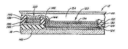
Referring now to Figures 3 and 4, they
illustrate in greater detail a configuration of light
sensitive element 120 and isolation device 122 in
725.2
~7~
`3
-J-8-
accordance with the present invention. Here, the
apparatus 12 includes the transparent or glass
substrate 18. Formed on the substrate 18 is a metal
pad which is electrically connected to a Y address
line 126. The metal pad 124 can be formed from
aluminum, chromium, or molybdenum, for example.
Formed on the metal pad 124 is the light
sensitive element 120 which can take the form of a
photovoltaic cell. The photovoltaic cell or light
sensitive elements 120 can include an amorphous
silicon alloy body having a first doped region 128, an
intrinsic region 130, and a second doped region 132.
The regions 128 and 132 are preferably opposite in
conductivity wherein the region 128 is p-tye and the
region 132 is n-type. Overlying the n-type regions
132 is a layer of a transparent conductor 134.
Photovoltaic cells of this type are fully disclosed,
for example, in the aforementioned U.S. Patent No.
4,226,898 and therefor need not be described in detail
herein.
The metal pad 124 not only forms an ohmic
contact with the light sensitive element 120 but in
addition~ serves to block light from reaching the back
side of the light sensitive element. This function of
the metai pad 124 is particularly important when the
scanning system is to be used in accordance with the
embodiment illustrated in Figure 1.
The isolation device 122, in accordance with
this embodiment, comprises a diode, also formed from
an amorphous silicon alloy having a p-type region 136,
an intrinsic region 138, and an n-type region 140.
The diode 122 is also formed on a metal pad 148 which
``` 725.2
_~9
is formed on a layer of a deposited insulator 142
which can be formed from, for example, silicon oxide
or silicon nitride. The diode 122 can be formed
during the same deposition as the photovoltaic device
120.
The diode 122 is coupled to the photovoltaic
cell 120 by an interconnect lead 144. Separating the
diode 122 from the photovoltaic cell 120 is a
deposited insulator 146 which can also be formed from
silicon oxide or silicon nitride.
The metal pad 148 is coupled to an X address
line 150. As can be noted in Figure 3, the X address
line 150 and the Y address line 126 are spaced apart
by the insulating layer 142. Because the address
lines cross at an angle and are separated from one
another, an insulated crossover point 152 is thereby
formed.
The structure of Figure 3 is completed by the
transparent cover member 68 which can be formed from
~0 glass. It is disposed over the diode and light
sensitive element and is adhered thereto by a
transparent adhesive which can fill the space 154. As
previously mentioned, the transparent adhesive
preferably has an index of refraction which matches
the index of refraction of the glass substrate 18 to
that of the cover member 68.
Referring now to Figure 5, it illustrates the
equivalent circuit diagram of the light sensitive
element 120, the isolating diode 122, and the address
lines 126 and 150. It can be noted that the
interconnect lead 144 connects the cathodes of the
photovoltaic cell 120 and diode 122 together. The
anode of the diode 122 is coupled to the X address
line 150 and the anode of the photovoltaic cell 120 is
coupled to the Y address line 126. It is to be
understood that the diodes formed by the isolation
725.2
Z7
~s
device 122 and the photovoltaic cell 120 can be
connected in an opposite polarity so that their anodes
rather than their cathodes touch.
In order to read the electrical
character,,tic of the photovoltaic cell 120, a
positive potential is applied to the X address line
150 and a negative potential is applied to the Y
address line 126. This forward biases the isolating
diode 122. If light is being reflected off of a light
portion of the document being scanned onto the
photovoltaic cell 120, a photogenerated current will
be produced within the cell 120 and will be detected
through the forward biased diode 122. However, if the
cell 120 is adjacent one of the dark portions of the
document, substantially no photogenerated current will
be produced by the cell 120. The difference between
- the two current levels can therefor be contrasted for
deriving an electrical signal representative of the
image adjacent the cell 120.
Referring now to Figure 6, it illustrates a
further configuration of light sensitive element 190
and isolation device 192. Here, the light sensitive
element takes the form of a photoresistor and the
isolating device 192 takes the form of a thin film
field effect transistor.
The apparatus 12 illustrated in Figure 6
includes a transparent substrate 18, which can be
formed from glass, for example. The gate of the thin
film field effect transistor 192 is first formed on
30 the substrate 18. A layer of insulating material 196
is then deposited over the gate 194 and the substrate
18. A metallic pad 198 is then formed over the
insulator 196 to form one contact of the light
sensitive element or photoresistor 190.
-~ 725.2
lZ7~ 1~7
~.
-2-~-
A substantially intrinsic amorphous silicon
alloy layer 200 is then deposited as shown for forming
the semiconductor of the thin film field effect
transistor 192 and the semiconductor of the
photoresistor 190. A layer 202 of n-type amorphous
silicon can then be formed over the intrinsic
amorphous silicon alloy 200 to enhance the ohmic
contact between the source and drain electrodes 204
and 206 with the amorphous silicon alloy 200. A layer
of a transparent conductor 20~ can be formed over the
amorphous silicon alloy 200 in contact with the
transistor electrode 26 and in a corresponding
configuration to the metal pad 198 to form the top
contact of the photoresistor 190. The structure of
Figure 6 is completed with the transparent cover 68
which can be formed from glass and a transparent
adhesive filling the space 210 as previously described.
As will be noted in Figure 6, the gate 194,
the electrode 204, and the bottom contact 198 of the
photoresistor 190 are all vertically separated from
one another. As a result, each of these elements can
be connected to respective address lines while being
insulated from one another. Figure 7 shows the
equivalent circuit diagram of the structure of Figure
6.
- In Figure 7, it can be noted that the
electrode 104 of the thin film field effect transistor
192 is coupled to an X address line 212. The gate 194
of the transistor 192 is coupled to a Y address line
240. The bottom contact 198 of the photoresistor 190
is coupled to a common potential such as ground by a
lead 216. As a result, the electrical conductivity of
the photoresistor 190 can be sensed by the application
of suitable potentials to the electrode 204 and gate
194 for turning the transistor 192 on. If light is
being reflected off of a light portion of a document
725.2
1L,2 7a3~LZ~
1,l
onto the photoresistor 190, a current will flow
between the transistor electrodes 204 and 206 which
can be sensed on the X address lead 212. However, if
the photoresistor 190 is immediately adjacent a dark
portion of the document, very little light will be
projected onto the photoresistor 190 so that
substantially no current will flow from the electro9de
204 to the electrode 206. In this manner, the
condition of the photoresistor 190 can be detected.
In accordance with the present invention,
electrical signals can be provided which represent the
color hues of an image. For example, each of the
light sources 96, 98, and 100 can include three
separate light sources each being arranged to e~it
light of a different primary color of red, green, and
blue. To generate the electrical signals
representative of the color hues of the image, the
image-bearing member 14 can be sequentially exposed to
the red, green, and blue light. During each exposure,
the light sensitive elements can be addressed. For
example, when the document 1~ is exposed to the red
light, those image portions thereof which include a
red color component will reflect red light onto the
light sensitive elements adjacent thereto. These
elements will effect a greater change in electrical
conductivity than those elements adjacent image
portions which do not include a red color component.
After this procedure is performed for each of the red,
green, and blue primary colors, the three electrical
signals provided from each light sensitive element
can be combined to derive both intensity and color hue
of the image.
Figures 8 and 9 are similar to Figures 3 and
6 discussed above respectively, except that tne
photosensors shown in Figures 8 and 9 are covered by
energy converting means 121 and 191, respecitively.
725.2
3~'X7~L'77
1~
-~2~-
These energy conversion means, when they are struck by
radiant energy of a first energy range, such as X-rays
or particle beams, emit radiation of a second energy
level which can be sensed by the energy sensitive
elements 120 and 190 of Figures 8 and 9, respectively.
The converter of energy 121 show;n in Figure
8 includes a continuous, transparent, insulating layer
121a formed of silicon dioxide. The layer 121a can
have a thickness on the order of 500 angstroms to 1
I0 micron. The converter 121 also includes
phosphorescent layer 121b forrnable of zinc sulfide
with a thickness between 1 micron and 100 microns with
20 microns preferred. The converter 121 also includes
a layer 121c of deposited metal such as aluminum that
is grounded at 121d. The thickness of the metal layer
121c is between 100 angstroms and lOnO angstroms with
300 angstr~ms being the preferred thickness. The
energy converter 121 converts X-rays, a form of
electromagnetic radiation with an intensity in a first
20 energy range into visible light, also a form of
electromagnetic energy, with an intensity in a second
energy range.
The structure of Figure 8 is completed by the
cover member 68 which is transparent to X-rays. It is
disposed over the energy converter 121 and is adhered
thereto by an adhesive which is transparent to X-rays
and preferably opaque to visible light.
The converter of energy 191 shown in Figure 9
is similar to the converter 121 just described. It
30 includes a silicon dioxide insulating layer l91a, a
phosphorescent layer l91b overlying the insulator l91a
and a grounded conductive layer l91c overlying the
phosphorescent layer l91b. A cover 68 can be affixed
to the conductive layer l91c.
725.2 ~ 7~27
c~
-2-~-
An alternate embodiment of the invention uses
an accelerated beam of electrons in place of the
X-rays disclosed above. In this alternate embodiment,
the electron beam can be deflected as in a raster
scanning system. As the deflected beam of electrons
impinges upon the sensor elements, such as the sensor
element of Figure 8, the energy of the electrons
excites the phosphorescent layer l91b causing it to
emit visible light as do the X-rays. The visible
light is detected by the element 190. Hence, as in
the embodiments of Figure 1-9, there is a conversion
from a first form of energy with an intensity in a
first range, that of the moving electrons, to a second
form of energy with an intensity in a second energy
range, that of emitted light.
In other embodiments of the invention, the
energy converting layer can be made by placing a
simple layer of fluorescent material over the
photosensors of the array, as is described below with
regard to an X-ray sensor used with the embodiment of
the present invention that integrates the radiation
incident upon its photosensors.
Now referring to Figure 10, the circuitry of
another embodiment of the present invention is shown
in schematic form. This embodiment of the invention
is designed to integrate the radiation which falls
upon its sensors, so as to greatly increase its
sensitivity. The apparatus 310 comprises an array of
photosensitive elements 312 formed as an integrated
circuit on a substrate, as shown in Figures 18 through
20~ below. For purposes of simplification, the array
of photosensitive elements 312 shown in Figure 10 is a
3 x 3 array. However, in most embodiments of the
invention much larger arrays are used.
` 725.2
~LZ7g~
2_o
The photosensitive elements 312 are formed at
the crossings of x lines 314 and y lines 316, with one
such photosensitive element connected between one x
line and one y line near the intersection of those two
lines. Each of the photosensitive elements includes
two back-to-back diodes, a photoresponsive diode 318
and a blocking diode 320. Each of these diodes has
associated with it a capacitance formed by its
electrodes. The two electrodes of the photodio~e 318
- 10 form a capacitor 322, and the two electrodes of the
blocking diode 320 form a capacitor 324. Since the
rectifying junctions of the diodes 318 and 320 are
located between the electrodes of the capacitors 322
and 324, respectively, those diodes operate as if they
were connected electrically in parallel with those
capacitors, as is illustrated schematically in Figure
10.
The y lines 316 are driven by column select
and drive circuitry 326. This circuitry provides 7ero
volts to all of the y lines except for a selected one,
to which it supplies +5 volts . The x lines 314 are
each connected through a pull-up resistor 328 to a +5
volt power supply 330. Each of the x lines 314 are
also connected to one input of a multiplexer 332. The
multiplexer 332 connects a selected one of the x lines
314 to its output 334, wnich is supplied to the input
of an amplifier 336. As is described below in greater
detail, the output 338 of the amplifier 336 provides a
signal which successively indicates the amount of
light incident upon each of the photosensitive
elements 312. The voltages to which the selected y
line 316 and the pull-up resistors 328 are connected
725.2
~;~Z~
.' \
~_
are both selected to be +5 volts in the embodiment
illustrated, since it is a convenient voltage commonly
associated with electronic circuitry. Of course,
other voltage values could be used without materially
affect~ g the invention's principles of operation.
Referring now to Figures lla through 17a and
Figures llb through 17b~ the operation of the
circuitry shown in Figure 10 will be described.
Figures llb through 17b show the voltages and current
10 flows in the photosensitive element 312a in the upper
left hand corner of the 3 x 3 array shown in Figure
10. The location of this element is indicated
schematically in Figures lla through 17a by the circle
surrounding the intersection between the upper most x
line 314a and the left most y line 316a.
The amplifier 336 is constructed so that it
drives its input to zero volts. As is well known in
the electronic arts, this can be accomplished by the
use of an operational amplifier with a resistive
20 feedback loop connected between its output and its
input. Such an amplifier is a current to voltage
converter, often called a transconductance amplifier.
The input voltage to such an amplifier typically
varies by less than .001 volts, and thus such voltage
variations can be ignored in this discussion. As a
result of the operation of amplifier 336, the
individual x line 314 which is connected at any given
moment by the multiplexer 332 to the input of that
amplifier has its voltage level driven to 0 volts.
30 All the other x lines 314 have their voltage level
pulled up to +5 volts by the pull-up resistors 328
connected to the +5 voltage supply 330.
Figures lla and llb show the state of the
photosensitive element 312a before any voltages have
been applied . In this initial state both the x line
314a and the y line 316a are at 0 volts, and thus the
`' 725.2
;27
-2-~-
two capacitors 322 and 324 are not yet charged, and
the connection 340 which joins them is at 0 volts.
When the column select and drive circuitry
326 and the multiplexer 332 select element 312a, the
select and drive circuitry 326 provides +5 volts to y
line 316a and 0 volts to all other y lines. During
the selection of element 312a, the amplifier 336
causes x line 314a to be driven to 0 volts, while all
the other x lines 314 are pulled to +5 volts through
the resistors 328. This is shown schematically in
Figure 12a. As is shown in Figure 12b, when this
voltage scheme is first applied to the element 312a,
current flows down the address line 316a and through
the blocking diode 320 and the connection 340 to
charge up the capacitor 322. The capacitive coupling
through capacitor 322 to the x line 314a, causes a
corresponding flow of current in line 314a toward the
input of the operational amplifier 336. As can be
seen from Figure 12b, the diode 320 is forward-biased
with regard to the flow of current from the y line
316a toward th~ capacitor 322. Thus it provides
relatively little impedance to such current. The
diode 320 is designed so that the capacitance 324 of
its electrodes is relatively small and thus can be
substantially neglected for purposes of determining
the operation of an element 312. However, as can be
seen from Figure 12b, the diode 318 is reverse-biased
relative to the current flowing from the y line 316a
toward the x line 314a. As a result, the diode 318
offers a high impedance to the flow of such current
across it, and thus the voltage drop across the diode
318 and the resulting charge across capacitor 322 is
substantially equal to the +5 volt difference applied
between lines 316a and 314a.
`~ 725.2
~27~ ~ ~7
~3
-2-3-
As is shown in Figures 13a and 13b, by the
end of its select period, the element 312a has its
capacitor 322 charged to ~5 volts, preventing any
further current from flowing from line 316a to line
314a other than a relatively small instantaneous
reverse leakage current across diode 313. This
discussion assumes for simplicity that the diodes have
no voltage drop when conducting in the forward
direction. The diodes actually do have a small
I0 voltage drop, but this fact does not materially affect
the principles of operation taught here.
In the embodiment of the invention shown in
- Figure 10, the column select and drive circuitry 326
and the multiplexer 332 are normally controlled to
select each of the photosensitive elements 312 in a
sequential scanning method in which each row, and each
elements within each row, are successively selected.
Figure 12a shows the state of the element 312a during
the period in which subsequent elements in its row
314a are being selected. During this period the x
line 314a is still held to 0 volts by the amplifier
336, but the select and drive circuitry 326 holds the
y line 316a to 0 volts, instead of the +5 volts to
which it is held when element 312a is selected.
However, the charge on the capacitor 322 is not
altered by this state of affairs, since the blocking
diode 320 is reverse-biased by the voltage applied
between contact 340 and line 316a, and thus it
substantially prevents the discharge of capacitor
322. Of course, there will be a small change in the
voltage on contact 340 when y line 316a changes
--- 725.2
-2~9-
voltage, due to the capacity divider effect between
capacitors 322 and 324. However, since the
capacitance 324 is much smaller than the capacitance
322, this change can be ignored in this discussion.
Tn any case, this change is compensated for when line
136a goes to ~5 volts on the next readout cycle.
The blocking diode 320 also prevents the
voltage on capacitor 322 from being discharged when
other rows are selected by multiplexer 332. As is
indicated in Figures lSa and 15b, when multiplexer 332
selects an x line other than the line 314a, the line
314a is pulled-up to +5 volts by one of the pull-up
resistors 328. It also shows that when the column
select and drive circuitry 326 selects a y line other
than the line 316a, the line 316a is supplied with 0
volts. This means that capactor 322 has +5 volts
connected to its side which was formerly at 0 volts,
driving the other side of the capacitor 322, connected
to contact 340, to ~10 volts, provided that the +5
volt charge previously placed on capacitor 322 has not
been lost. During this state the blocking diode 320
inhibits charge on capacitor 322 from being lost to
the y line 316a, which is at 0 volts.
Figures 16a and 16b show what happens when
the y line 316a is selected during a period when an x
line other than line 314a is selected. In this case
both the x and y lines of the element 312a are
supplied with a positive ~5 volts. As a result, the
contact 340 is driven +10 volts, provided capacitor
3Q 322 still has the ~5 volts charge initially supplied
it. During this state the blocking diode 320
continues to inhibit the charge on capacitor 322 from
being lost to the y line 316a.
Figure 17 shows what happens when the element
312a is again selected by both the multiplexer 332 and
the select and drive circuit 326. In this case
725.
~ z~7~ ~ ~t~
~ .,
voltages are again applied to the element 312a which
are identical to those shown in Figure 12b. However,
no current flows to capacitor 322 unless that
capacitor has lost charge since the last time it was
selected, because unless such charge has been lost,
the capacitor 322 already has a voltage equal to the
voltage difference between y line 316a and x line 314a.
However, if light hits the diode 318 between
the successive rechargings of its associated
capacitance 322, something will be done to discharge
that capacitance. This is because the diodes 318 are
photoresponsive diodes, in which the reverse leakage
current is greatly increased in the presence of
light. When light hits the semiconductor material of
such a ~iode, it generates electron-hole pairs which
are swept by the field across such a diode in a
direction that discharges the voltage generating that
field. The more the light strikes a diode 318
between the recharging of its associated capacitor
322, the more the charge on that capacitor is lost.
As a result of this lost charge, the voltage left on
capacitor 322 is less than the voltage applied across
it when the capacitor is next recharged, causing
current to flow onto the capacitor 322 during its
recharging. Because of capacitive coupling across
capacitor 322, current flow to capacitor during its
recharging causes current to flow in the capacitor's x
line 314 to the amplifier 336, creating an signal at
the output of that amplifier. The amount of such
current is in proportion to the amount by which the
capacitor 322 has been discharged by incident
radiation since its previous recharging.
All of the photoresponsive elements 312
function in a manner similar to that of the element
312a just described. Thus the signal at the output of
amplifier 336 varies in correspondence to the
-` 725. 2
~ k,
-~3~-
magnitude and time incidence of radiation incident
upon the semiconductor material of each diode 31
during the entire period between its successive
rechargings. In other words, the signal which results
when a given photodiode is selected is not an
instantaneous function of the amount of light falling
on that photodiode during its selection, but rather is
a function of all the radiation incident upon that
photodiode during the entire period since its previous
recharging. As a result, the apparatus of the present
invention provides a much greater sensitivity and a
much greater immunity to noise.
The current flow during the recharging of a
given capacitor 322 is not constant. Instead it
varies during the recharging period, with the amount
of such current increasing rapidly to a maximum value
at the beginning of each recharging period and then
decreasing more slowly as the voltage on the capacitor
approaches the voltage applied across it. Once the
capacjtor is completely charged, the current is
limited to the relatively small instantaneous value of
the reverse leakage current across its associated
diode 318. Thus, the output signal produced by
amplifier 336 in association with the selection of a
given picture element is not a constant value, but
rather a current pulse starting with a relatively
rapid increase and ending with a relatively slow
decrease. The actual rates of the increase and
decrease depend upon many parameters, among them, the
impedance of the driving circuitry, stray capacitance,
and the time response characteristic of the diodes.
This output is used in different ways in
different embodiments of the invention to indicate the
amount of light whicn has hit each of the
photosensitive elements. In some embodiments the
output of amplifier 336 is integrated over the
r
` 725.2
~7~1~
~,1
recharging period of each photosensitive element by
means of an integrating amplifier. This is perhaps
the most accurate method. In other embodiments, a
sample and hold circuit i5 used to sample the
magnitude of the output of amplifier 336 at a
specified time during the recharging period of each
picture element, such as the time at which that signal
is at its maximum value. The resulting sampled value
is then used as the indication of the amount of light
which has hit the associated photoresponsive element
since its last recharging. In other embodiments, the
output of amplifier 336 is fed as a video signal to a
cathode-ray-tube having a scanning pattern and rate
similar to the array of photosensors 312. In such an
embodiment, even though the amplitude of the video
signal varies over the portion of a video line
associated with a given photosensitive element, this
is normally of little concern since the corresponding
picture elements are close together on the CRT screen,
and since such high frequency variations in the video
signal can be reduced by the use of a low pass filter.
Referring now to Figures 18, 19 and 20, a
radiation sensing appartus formed as an integrated
circuit according to the present invention is shown.
The radiation sensing apparatus shown in those figures
comprises a substrate 341 formed of glass. In
alternate embodiments of the invention other
insulating substrates can be used, such as substrates
formed of conductive materials, for example, stainless
steel, coated with an insulator to provide the
necessary electrical isolation for devices formed
their surface. A layer 342 formed of molybdenum or
another metal which forms a good ohmic contact with P~
type amorphous silicon alloys is deposited upon the
substrate 341 by means such as sputtering, and then is
patterned by photolithographic techniques to form the
3L `'-~t~
- ~3 -
y address lines 316, the bottom electrodes 344 of the
photoresponsive diode 318, and an extension of that
bottom electrode which forms part of the address lines
314. Once the metal layer 342 has been patterned,
three successive layers of amorphous semiconductor
material are deposited upon the substrate 340, first a
P+ layer 346 having a thickness of approximately 250
angstroms, then a substantially intrinsic, or I layer 348
having a thickness of approximately 3,500 angstroms, and
then an N+ layer 350 having a thickness of approximately
250 angstroms. The deposited semiconductor material is
preferably an amorphous semiconductor alloy including
silicon. The amorphous silicon alloy can also include
hydrogen and/or fluorine and can be deposited by plasma
assisted chemical vapor deposition.
Amorphous silicon alloys can be deposited in
multiple layers over large area substrates to form
structures such as the integrated circuit shown in
Figures 18,- 19 and 20 in high volume, continuous
20 processing systems. Continuous processing systems of
this kind are disclosed, for example, in U.S. Patent
No. 4,400,409, issued August 23, 1983 for "A Method of
Making P-Doped Silicon Films and Devices Made Therefrom";
U.S. Patent No. 4,410,558, issued October 18, 1983 for
"Continuous Amorphous Solar Cell Production Systems";
U.S.Patent No. 4,438,723 issued March 27, 1984 for
"Multiple Chamber Deposition and Isolation System and
Method". As disclosed in these patents, a substrate may
be continuously advanced through a succession of deposition
jb/ye
27
chambers, wherein each chamber is dedicated to the
deposition of a specific material.
For example, in making the P-I-N layers 346,
348 and 350 shown in Figures 19 and 20, a single
deposition chamber can be usecl for batch processing, or
preferably, a multiple chamber system can be used
wherein a first chamber is used for depositing a P+
type amorphous silicon alloy, a second chamber is used
for depositing an intrinsic amorphous silicon alloy,
and a third chamber is used for depositing a N+ type
of amorphous silicon alloy. Since each deposited alloy,
and especially the intrinsic alloy, must be of high
purity, the deposition environment in the intrinsic
deposition chamber is preferably isolated from
undesirable doping constituents within the other
chambers to provide the diffusion of doping constituents
into the intrinsic chamber. Where the systems are
primarily concerned with the production of photovoltaic
cells, isolation between the chambers is accomplished
by gas gates through which unidirectional gas flow is
established and through which an inert gas may be swept
about the web of substrate material. In the previously
mentioned patents, deposition of the amorphous silicon
alloy material onto the large area continuous substrate
is accomplished by glow discharge decomposition process
gases. Among these processes, radio frequency energy
glow discharge processes have been found to be suitable
for the continuous production of amorphous semiconductor
jb/ye
-- 3~ ~z~7g~,~7
- ~3~ -
An Improved process for making amorphous semiconductor
alloys and devices is disclosed in applicant's U.S. Patent
No. 4,517,223, issued May 14, 1985 for "A Method of Making
Amorphous Semiconductor Alloys and Devices Using Microwave
Energy". This process utilizes microwave energy to decompose
the reaction gases to cause deposition of improved amorphous
semiconductor materials. This process provides substantially
increased deposition rates and reaction gas feed stock
utilization. MicrowaYe glow discharge processes can also
be utilized in high volume mass production of devices.
After the P-I-N layers 346, 348 and 350 have
been deposited across the entire surface of the sub-
strate 341, a thin layer 352 of a transparent conductor
such as indium tin oxide is deposited on top of the N+
layer 350. Such a layer is preverably between 200 and
500 angstroms thick. Once the multilayered structure
comprised of the P+ layer 346, the intrinsic layer 348
the N+ layer 350 and the indium tin oxide layer 352
- has been formed over the entire surface of the
substrate 340, photolithographic techniques are used
to etch that combined layer into an array of diode
pairs with one such diode pair for each photosensitive
element 312 to be formed. Each of the diode pairs
includes a large diode forming the photodiode 318 of
its photosensitive element and having an area of
approximately 200 microns by 200 microns. Each of
the diode pairs also includes a much
jb/ye
r~
. "
~ .
~~`- 725.2
-36-
smaller diode forming the blocking diode 320 and
having an area of approximately 30 microns by 30
microns. The bottom electrode of the photodiode 318
is formed by the molybdenum electrode 344, and the top
electrode of that diode is formed by the ITO layer
352. Similarly, the bottom electrode of the blocking
diode 320 is formed by a portion of the address line
316 and the top electrode of that diode is formed by a
portion of the ITO layer 352. The relatively large
overlapping area of the electrodes of photodiode 318
p ovide that diode with a relatively large
capacitance. The much smaller area of the blocking
diode 320 causes the capacitance 324 associated with
its top and bottom electrodes to be much less.
Once the diodes 318 and 320 have been formed,
the entire substrate 340 is covered with a thin
transparent insulating layer 354. Preferably this
insulating layer 354 is formed of polyimide, which can
be placed over the substrate 340 and the structures
formed upon it by roller, extrusion, or spin-coating.
Alternatively, the insulating material in layer 354
could be formed from a deposited insulating material,
such as silicon oxide or silicon nitride. Once the
transparent layer 354 has been deposited,
photolithographic techniques are used to form a
contact opening 356 through a portion of layer 354 on
top of photodiode 318 and a similar contact opening
358 through a portion of layer 354 on top of blocking
diode 320. Similarly, a contact opening 360 is formed
over the bottom right hand corner (as shown in Figure
18~ of the bottom electrode 344 of photodiode 318, and
another contact opening 362 is formed in the leftmost
extension (as shown in Figure 18) of the bottom
electrode 344 which forms part of its associated x
line 314. When these contact openings have been
formed, a layer of metal such as aluminum is deposited
., .
' ' ' ' ~
` 725.2
lZ'7~'7
-~z
-~7-
and patterned to form the connection 340 between
openings 356 and 358 of each diode pair, connecting
the cathodes of diodes 318 and 320. This top metal
layer is also patterned to form a connecting link 364
between adjacent contact openings 360 and 362, so as
to connect all of the bottom electrodes of the diodes
318 in a given row, and thus complete the address line
314 associated with that row. The metal contact 340
covers the blocking diode 320 from light, although
10 this is not clearly shown in Figure 20, in which the
vertical scale has been greatly exaggerated for
purposes of illustration.
Once the integrated circuit has been formed
in the manner described, it is preferable to coat it
with a passivation layer (not shown), such as one
formed of polyimide, to protect the top metal links
340 and 364 from oxidation.
The structure shown in Figures 18 through 20
forms an array of photosensitive elements 312 of the
20 type shown in Figure 10. Since amorphous silicon
alloys have very low dark conductivities and very high
photoconductivities, the photodiodes 318 form very
sensitive photoresponsive devices. As a result, the
structure shown in Figures 18 through 20 forms an
excellent photosensitive array.
Referring now to Figure 21, an alternative
embodiment of the invention is shown which is also
electrically equivalent to the schematic diagram shown
in Figure 10. The structure in Figure 21 is identical
30 to that in Figure 20, except that its address lines
316, which form the bottom electrodes of its blocking
diodes 320, and the bottom electrodes 344 of its
photodiodes 318 are formed of a metal, such as
palladium or platinum, which forms a Schottky barrier
when placed in contact with intrinsic amorphous
silicon. The structure of Figure 21 is also
i
725.2
t~
-3~-
distinguished from that shown in Figure 20 by having
only one layer 366 of intrinsic amorphous
semiconductor material between the electrodes of its
diodes 318 and 320, rather than the three P-I -N 1 ayers
346, 348 and 350 as in Figure 20. The platinum or
palladium metal of the bottom electrodes of the diodes
318 and 320 form the anodes of those diodes, and the
intrinsic silicon alloy layer 366 forms the cathodes,
causing the diodes 318 and 320 shown in Figure 21 to
I0 have the same polarity as the PIN diodes shown in
Figure 20. In embodiments in which it is deSired to
improve the ohmic nature of the contact between the
top IT0 electrodes 352 and the intrinsic layer 366, a
thin layer of N+ silicon alloy is placed between that
IT0 electrode and the intrinsic layer.
Figure 22 shows another embodiment of the
invention, which is identical to that in Figure 20
except the diode 318 has been replaced with a
photoresistor 368. The photoresistor 368 is comprised
of the single layer 348 of intrinsic amorphous silicon
alloy, placed between a bottom metal electrode 344 and
a top IT0 electrode 352, both identical to those shown
Figure 20. Photolithographic techniques prevent the
P+ and N~ layers 346 and 350 used in the P-I-N
blocking diode 320 from being deposited between the
electrodes of photoresistor 368. Thus, the
photoresistor 68 does not have diode characteristics.
But since the intrinsic amorphous silicon alloy of
layer 348 has a high dark resistivity while exhibiting
a substantial photoconductivity, the device 368
functions much like the diode 318 for the purpose of
the present invention. That is, in the absence of
light it tends to maintain electrical charge placed
upon the capacitor 322 formed by its top and bottom
electrodes, and it discharges that electric charge in
proportion to the amount of light which falls upon it.
~ ` 725.2
,'7~3~7
.~y
-39-
- Figure 23 shows an embodiment of the present
invention for sensing x-ray images. This apparatus is
virtually identical to that shown in Figure 20, with
the exception that a layer of fluorescent material
several hundred microns thiCk has been placed over
it. Suitable fluroescent materials for such a layer
include lanthanum oxysulfide with terbium, gadolinium
oxysulfide with terbium, ytterbium oxysulfide with
terbium, barium fluorochloride with europium,
I0 ytterbium oxides with gadolinium, or barium
orthophosphate with europium. The thickness of this
layer is not drawn to scale for purposes of
convenience. When x-ray radiation falls upon the
fluorescent layer 370 it generates light photons
having a frequency which causes the generation of
charge carriers in the photodiodes 318 of its
associated photoresponsive elements. As a result, the
amount of current required to recharge the capacitance
of each of the photodiodes 18 is a function of the
amount of x-ray radiation incident upon the portion of
the fluorescent layer 370 overlying each such diode.
Thus an array of photoresponsive elements 312 coated
with the fluorescent layer 370 enables x-ray images to
be electronically sensed.
In certain uses of x-ray imaging, such as
certain medical uses, it is often desirable to have
image sensing elements which are accurate over a broad
dynamic range. With the present invention such
accuracy can be achieved by the use of calibration
techniques which measures the readings produced by
each photosensitive element 312 in response to known
levels of incident radiation and use a computer having
such calibration information to adjust the output of
each photosensitive element in correspondence with
such calibration data. For maximum results such
calibration should compensate not only for the
` 725.2 1~ 7
,~,~
.
differing photoresponsive characteristics of each
photodiode 318, but also for the light-independent
reverse leakage current of each such photodiode.
Typically photodiodes of the type described in regard
to Figure 18 through 20 have a leakage current in the
dark which is less than one thousandth that of the
photo-induced leakage current which they generate in
normal room light. This difference is great enough so
that the output signal produced can be used for many
lo purposes without compensation for such
light-independent leakage current. But in situations
where a high dynamic range of light sensitivity is
required, a computer is used to adjust for such
leakage current.
In order to achieve a desired range of light
sensitivity it is also important to choose the proper
length of time between the recharging of the picture
elements 312. A good length of time is one that is
just long enough to allow the recharging voltage
placed on the element to be completely discharged by
light at the top end of the range of light intensities
which the element is intended to measure. If the time
is shorter than this, the time during which a
photodiode has to integrate light incident upon it
will not be enough to produce a maximum signal. If
the time is longer, the capacitor 322 wili be totally
discharged by a whole sub-range of light intensities
falling within the range of intensities to be
measured, having the undesirable effect of making it
impossible to distinguish between any such light
intensities falling within that sub-range. If the
time between recharging is made extremely long, the
light-independent leakage current will totally
discharge the capacitors 322 by itself, making it
impossible to measure any signal produced by the
incidence of light on the photodiodes,
725.2 3LZ7~ 7
In some large arrays constructed in the
general manner shown in Figure 10, the time between
recharging is reduced by connecting the pull-up
resistors 328 attached to each x line to ground
instead of to +5 volts. This causes all the
photoresponsive elements 312 in a given column to be
recharged in parallel each time the y line 316
associated with that column is supplied with ~5
volts. As a result, each element 312 is recharged
Io once during the scanning of each row. The resistance
of the resistors 328 is sufficiently large so that the
recharging current which flows -to ground from
unselected x lines is isolated from the recharging
current which flows to the amplifier 336 from the
selected x line. This enables the recharging currents
in the selected row to be read independently of the
recharging currents in non-seleçted rows. This
recharging method is particularly suitable for use
with large high-resolution arrays used in contact
20 document copier of the type discussed below.
One of the advantages of the present
invention is that it enables a sensing apparatus to be
constructed in which the individual elements can be
randomly addressed. For example, in the apparatus
disclosed in Figure 10, any given photoresponsive
element 312 can be read by: a) selecting its
associated x and y lines to charge it, b) subsequently
selecting those lines again after a known period of
time has elapsed to recharge it, and, c) measuring the
30 current that flows during such recharging, This
random addressability means that the time between
recharging can be selectively varied over different
portions of the display to vary the range of light
intensity over which those portions are responsive.
-~' 725.2 ~2~
3~1
-~2-
Such random addressibility also allows a large array
to be scanned quickly by reading only a representative
sample of its photoresponsive elements, while allowing
the option for more detailed image scanning when and
where desired.
Figure 24 shows an image sensing apparatus ..
380 according to an embodiment of the invention which
is designed for use in forming images of documents
placed in close proximity to its array of
I0 photosensitive elements. The apparatus 380 includes
an array of photosensitive elements 312 similar to
those shown in Figure 20. However, the glass
substrate 340 of apparatus 380 is substantially
thicker than shown in Figure 20, so that documents and
books can be placed upon it without its being broken
by their weight. In addition, the apparatus 380 has
placed over its insulating layer 354 and its top metal
contacts 340 and 364 a layer 382 of sputtered silicon
dioxide (SiO2) or silicon nitride (Si3Cn4) to
form a hard, transparent, substantially flat oxide
layer approximately 100 microns thick. The apparatus
380 shown in Figure 24 is designed for copying opaque
documents, such as the document 384 partially shown in
Figure 24. The photosensitive elements 312 are spaced
sufficiently far apart to allow a substantial amount
of the light entering the substrate 340 from its
backside, as indicated by arrows in Figure 24, to pass
between such elements, and illuminate the surface of a
document facing the transparent oxide surface 382.
Each individual photosensitive element 312 responds
primarily to the amount of light reflected from the
portion of document 384 placed closest to it. For
example, in Figure 24 the document 384 is shown as
having a darkened portion 386 upon its bottom surface,
such as part of an inked letter of text. Since
relatively little light is reflected from this
725.2 ~ 7
~3
darkened portion 386, the photosensitive elements 312
beneath it receive little reflected light. However, a
relatively large amount of light is reflected from the
light portion 388 on the bottom surface of document
384, and thus the photsensitive elements 312 below
that portion receive more light. It is important that
the metal which forms the bottom electrodes of the
diode5 318 and 320 be over 2,000 angstroms thick, so
as to prevent radiation from below those diodes from
0 impinging directly upon them.
In order to form accurate copies of documents
such as business letters and pages from books and
magazines, it is desirable that the sensing apparatus
380 have a resolution of at least 4 points per
millimeter, and, preferably, of 8 points per
millimeter. To form a sensor with a resolution of 8
points per millimeter the photosensitive elements 312
should be spaced every 125 microns, and the oxide
layer 382 should be no more than approximately 100
microns thick. One of the advantages of the present
invention is that it can be used to form an array of
photosensitive elements that is at least 11" long and
8-1/2" wide as a single integrated circuit. This is
because the deposited semiconductor materials used to
form the image sensing apparatus of the present
invention can be deposited over large areas, as is
described above, and do not require crystalline
substrates, which are presently limited in size. Thus
the present invention makes it possible to make a
solid state document imaging device with no moving
parts, with the imaging element formed as one
integrated circuit on a single glass substrate.
Referring now to Figure 25, an incident
radiation sensing apparatus 390 according to the
present invention is shown in schematic formr The
apparatus 390 includes a focusing means, such as a
`~`~ 725.2 ~ .7
~,ct
-~4-~-
lens 392 for focusing a light image upon an array 394
of photosensitive elements 312. In the embodiment
shown, the array of photosensitive elements 312 is a
structure such as that shown in Figures 18 through
20. Experiments have shown that such photosensitive
arrays have sufficient sensitivity to produce images
of objects illuminated in normal room light when
scanned at a video rate and used in conjunction with a
lens having an aperture of F4. Thus the present
invention is suitable for use in video cameras as well
as electronic still cameras.
From the foregoing it is apparent that
incident radiation sensing apparatuses according to
the present invention can be employed in a variety of
radiation sensing applications including not only
X-ray imaging, document copying, an~ electronic
photographs, but also any other application in which
it is desirable to sense a spatial distribution of
radiation. It is recognized, of course, that those
skilled in the art may make various modifications or
additions to the preferred embodiments chosen to
illustrate the invention without departing from the
spirit and scope of the present contribution to the
art.
Moreover, the scope of protection is not
intended to be limited by the above described
embodiment and exemplifications, but solely by the
claims appended hereto.