Note: Descriptions are shown in the official language in which they were submitted.
01 This invention relates to telephone
02 systems in general, and more particularly to a digital
03 signal processing system for use as a digital service
04 unit within a communications switching system.
05 Digital service units (DSUs) are used in
06 modern day communications systems such as PABXs, to
07 provide such features as -tone genera~ion, tone
08 detection, and conferencing.
09 Prior art DSUs typically incorporated a
plurali-ty of circuits dedicated to provision of
11 respective ones of the aforementioned features. Tone
12 detection circuitry, tone generation circuitry and
13 call conferencing circuits were typically all disposed
14 on respective printed circuit boards comprising
discrete components, and were rack mounted in a
16 cabinet, such as a PABX equipment cabinet.
17 The prior art circuitry typically occupied
18 considerable circuit board area, and was characterized
19 by high cost, circuit complexity and little or no
capacity for expansion. In addition, many of the
21 prior art DSUs employed analog circuitry which was
22 prone to distortion and low accuracy performance due
23 to temperature drift, etc.
24 According to the present invention, a
digital~signal processing system is provided for
26 implementing features such as digital tone generation,
27 digital conferencing, DTMF tone detection, progress
28 tone detection, and speech synthesis, as well as
29 others. According to a preferred embodiment, the
~eatures are implemented digitally via a dedicated
31 digital signal processing (DSP~ module comprised of a
32 digital signal processing chip, one or more random
33 access memories and a programmabl~ logic array ~ULA)
34 embodying DSP support logic circuitry for interfacing
the DSP chip. One or more o~ such DSP modules are
3~ connected via time divided digital signal links to a
37 dedicated digital crosspoint (DX) switch.
38 - 1 -
d~
~;~t79~33
01 A central processor or main controller supervises
02 interaction between the DX switch and the DSP ~odules.
03 Unlike prior art DSUs which typically
04 employed dedicated paths for circuit switching and
05 messaging, according to the present invention circuit
06 switching and message communication are combined on
07 one or more shared DX links wherein the portions of
08 the link bandwidth dedicated to messaging and circuit
09 switching are controlled by the main con~roller and
are dependent o~ which of the service eatures is
11 being implemented. For instance, in the event the
12 desired service ~eature requires a large amount of
13 signal processing computation time to implement but
14 has low input/output signal traffic, then relatively
few circuit switch channels are allocated. However, if
16 the feature requires little computation power but wide
17 input/output bandwidth, a large number of circuit
18 switch channels are allocated.
19 The DX switch is addressed by the main
controller via parallel address and data ports in
21 order to dynamically allocate channels for
22 establishing message and circuit switch paths to each
23 DSP module, and an interrupt handshaking scheme is
24 implemented between the DX switch and DSP modules for
controlling transmission of message information
26 packets therebetween. The packets can be either
27 applications programs ~or downloading to one or more
28 of the DSP modules, or interrupt and control signals
29 for supervising the timing and execution o~ the
programs.
31 An important characteristic of the present
32 invention is that a digital DX switch is utilized in
33 connection with the one or more DSP modules ~or
34 providing combined message and circuit switching via
dynamically allocated message and circuit switch
36 channels. Thus, a plurality of service fea~ures are
37 accommodated with a minimum of circuit complexity and
38 - 2 -
~;~79;~ 3~
1 cost.
2 According to an embodiment of the present
3 invention, a digital signal processing system for use
4 in a communication system connected to a plurality o~
S input/output ports is comprised of a main contro}ler
6 apparatus for transmitting and receiving message
7 signals, and a digital signal processing apparatus
8 for implementing one or more service features
9 characterized by one or both of transmission and
reception of PCM and message signals. A digital
11 switching apparatus is connected to the main
12 controller apparatus, digital signal processing
13 apparatus, and input/output ports, for
14 bidirectionally translating PCM and message signals
therebetween, via one or more time divided
16 communication lihks under control of the main
17 controller circuit. Further apparatus dynamically
18 allocates predetermined channels of the one or more
19 time divided communication links for PCM and message
signal translation, wherein the proportion of
21 channels allotted to PCM and message signal
22 translation is dependent on which of the one or more
23 service features is being implemented, thereby
24 maintaining high signal bandwidth efficiency of the
PCM and message signal translation.
26
27
28
29
31
32
33
34 - 3 -
~ ~,7~3~3;~
01 A better understanding oE the present
02 invention will be obtained with reference to the
03 detailed description helow in conjunction with the
04 following drawings, in which:
05 Figure 1 is a block diagram oF a digital
06 signal processing system in accordance with the
07 present invention,
0~ Figure 2 is a block schematic diagrarn of a
o9 main controller, circuit switch matrix and dedicated
digital DX switch according to the preferred
11 embodiment of the present invention, and
12 Figure 3 is a block schematic diagram of a
13 digital signal processing module according to the
14 preferred embodiment.
With reference to Figure 1, a main
16 controller 1 is shown connected to a circuit switch
17 matrix 3 having a plurality of input/output ports such
18 as line and trunk circuits SA-SC and a peripheral
19 switch matrix 5D connected thereto. A subscriber set
7 and a data terminal 9 are shown connected to a
21 representative one of the line circuits SA via
22 bidirectional PCM links llA and 11B. PCM links llA
23 can be replaced by well known balanced bidirectional
24 telephone lines in the event that the subscriber set 7
is a standard 500 type telephone set. In this case,
26 the line circuit 5A typically also includes a
27 digital-to-analog and analog-to-digital converter for
28 translating between analog signals on the telephone
29 line aRd PCM encoded signals transmitted to and from
the circuit switch matrix 3.
31 Trunk lines may be connected to the trunk
32 circuit SB extending from a telephone central office
33 via the lines llC, and digital trunks (such as the
34 industry standard Tl trunk) may be connected to the
digital trunk circuit 5C. The peripheral switch
36 matrix 5D may be connected via links llE to additional
37 - 3a -
9~
01 expansion line and trunk circui-ts in a well known
02 manner.
03 A plurality o~ DSP modules 13 are
04 connected via dedicated PCM links 15 to the circuit
05 switch matrix 3. Each of the DSP modules 13 has a
06 control output thereof Eor generating an interrupt
07 signal TMSINT 5 for interrupting the main controller
08 1. The TMSINT 5 signal output from individual ones of
09 the DSP modules 13 is a high impedance output, and
each signal is applied to a common interrupt line
11 ~orming a logic OR function. The main controller 1
12 generates respective interrupt clear signals for
13 resetting interrupts generated by the DSP modules 13.
14 In operation, the main controller 1
configures a predetermined switching element or DX
16 switch (discussed below with reference to Figure 2) of
17 the circuit switch matrix 3 for dynamically allocating
18 predetermined PCM channels of the shared links 15 for
19 establishing a message signal path between the circuit
switch matrix 3 and each DSP module 13. An interrupt
21 handshaking scheme is utilized to establish
22 communication between the main controller 1 and DSP
23 modules 13 utilizing the aforementioned interrupt
24 signals.
For example, a predetermined DSP module 13
26 can generate a TMSINT 5 interrupt control sign~l for
27 application to the INT input of the main controller
28 1. In response, the main controller gen~rates a
29 message signal packet for transmission along a
dedicated message signal channel of a predetermined
31 dedicated message signal channel of a predetermined
32 one o~ the PCM links 15 via circuit switch matrix 3,
33 for storage in an internal memory of the DSP module
34 13. The main controller 1 then generates an
appropriate clear interrupt signal via a CLRINT output
36 thereo-f for causing the selected DSP module 13 to
37 reset its TMSINT 5 signal output- The DSP module 13
38 - 4 -
01 then generates another TMSINT 5 interrupt signal for
02 causing the main controller l to transmit a second
03 message signal packet, and the procedure is repeated
04 until an en-tire program has been downloaded.
05 The message signal packets can be, for
06 instance, in the ~orm of an applications program code
07 for execution by one or more of the DSP modules 13,
08 resulting in implementation of a predetermined service
09 feature.
Once the internal memory o~ the DSP module
ll 13 has been loaded with the applications pxogram, the
12 code is executed by the DSP module for performing one
13 of either tone plant, digital conferencing, DTMF or
14 ATD tone detection, speech synthesis, etc.
For example, in order to implement the
16 speech synthesis service feature, one or more encoded
17 messages are first stored on a disk (not shown), such
18 as Winchester disk connected to the main controller
l9 1. The main controller 1 then transmits the encoded
messages to a predetermined one of the DSP modules 13
21 via allocated message channels of the PCM links 15
22 through circuit switch matrix 3. The selected DSP
23 module 13 executes the stored applications program and
24 converts the encoded messages into A-law or ~-law
encoded PCM signals and transmits the PCM signals via
26 further allocated channels (circuit switch channels)
27 of the PCM links 15 to one or more of the line or
28 trunk circuits 5A-5D.
29 Since the PCM channels are dynamically
allocated, as many or as ~ew of the channels are
31 utilized by a predetermined DSP module 13 as required
32 for implementing the particular service feature.
33 Thus, if the service feature requires considerable
34 computation time for the applications program to be
executed, the channel bandwidth is low (eg. four or
36 five allocated circuit switch channels are used for
37 tone detection~. However, if the DSP program requires
38 - 5 -
:
:
. : ''
33
01 little computation time but high signal throughput, a
02 large number of circuit switch channels may be
03 allocated, (for example forty-two channels are used
04 for implementing the tone plant feature).
05 As a further example, digital conferencing
06 can be implemented according -to the pxesent invention,
07 by programming a predetermined one of the DSP module~
08 13 for receiving voice or tone signal samples erom
09 predete.rmined ones of the line, trunk or peripheral
matrix circuits 5~-5D via the circuit switch matrix 3
11 and dedica-ted circuit switch channels of PCM links
12 15. 'Fhe DSP module 13 detects the "loudest" one of
13 the signal samples (i.e. the sample having the largest
14 magnitude) and sends that sample to each of the signal
sources connected to the line or trunk circuits 5A-5D
16 except for the signal source from which it was
17 generated. The second loudest signal sample is then
1~ transmitted to the source of the loudest siynal
19 sample.
The tone detection feature of the present
21 invention can be implemented by a predetermined one or
22 more of the DSP modules 13 by receiving a number of
23 tone signal samples from one or more of the circuits
24 5A-5D via circuit switch matrix 3 and dedicated
circuit switch channels of the PCM links 15, and
26 performing thereon. A well known tone detection
27 algorithm performs a discrete Fourier transform on the
28 received tone samples and generates a message signal
29 along a further dedicated message signal channel of
the PCM lin~s 15 to the main controller 1, indicative
31 of whether or not a predetermined DTMF tone is
32 present.
33 Additional features can be performed by
34 the digital signal processing system of the present
invention. For example, type-written messages from a
36 data terminal, such as data terminal 9, can be
37 transmitted via line circuit 5A, through circuit
38 - 6 -
93~33
01 switch matrix 3, and along a dedicated message channel
02 o-E the PCM link 15 to a predetermined one o~ -the DSP
03 modules 13. In response, the DSP module 13 can
04 implement a text-to-speech conversion algorithm or a
05 direct speech synthesis algorithm for generating
06 "canned messages" along further circuit switch
07 channels of the PCM links 15 via circuit switch matrix
08 3 to other ones of the subscriber sets 7 or -terminals
09 connected to the input/output ports ~A-5D.
Thus, the digital signal processing system
11 as illustrated in Figure 1 provides many o the same
12 features as prior art digital service units (DSUs),
13 plus many more. However, as discussed above, prior
14 art DSUs typically require dedicated paths for circuit
switch signals and message signals, whereas according
16 to the present invention both functions are
17 dynamically allocated between single or multiple PCM
18 links 15, wherein the proportion of channels devoted
19 to either of message or circuit switch signalling
varies as the application demands.
21 An important element of the system
22 embodying the present invention is the DX switch,
23 discussed in greater detail below with reference to
24 Figure 2. The DX switch is a com~ined program~able
time and space switching circuit utilized within the
26 circuit switch matrix 3 for dynamically allocating PCM
27 channels of the links 15 to the DSP modules 13 in
28 order to support simultaneous combined message and
29 circuit switch signalling.
A detailed description of the DX switch
31 can be found in Canadian patent No. 1,171,946 entitled
32 TIME DIVISION SWITCHING SYSTEM, issued July 31, 1984
33 to Mitel Corporation, to which the reader is referred.
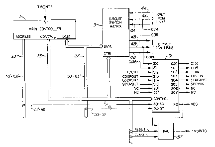
34 With reference to Figure 2, the main
controller 1 is shown in greater detail having an
36 address bus 23, control bus 25 and data bus 27
37 connected thereto. The main controller typically
38 - 7 -
01 includes a microprocessor, such as the ~et~nlJ~a
02 MC68020 microprocessor in conjunction with support
03 logic circui~ry and one or more disk drives and RAM
04 memory circuits (not shown). According to a
05 successful prototype of the present invention, 4
06 megabytes of RAM were provided and -the MC68020 was
07 utilized for controlling a communication switching
08 system with up to 300 lines, (such as the lines or
09 links denoted as llA-llE in Figure 1).
According to the preferred embodiment, the
11 address bus 23 is comprised of 32 address lines
12 A0'-A31', the data bus 27 is comprised of 32 data
13 lines D0 '-D31 ' and the control bus 25 is comprised of
14 a plurality of well known control signal carrying
lines, such as READ/WRITE, CHIP ENABLE, RESET, and
16 various timing and clock signals.
17 A PAL~ device 61 is connected to
18 predetermined lines of the control bus 25 designated
19 RESET, TMSG, CLKOUT 0, CLKOUT 1 and CLKOUT 2, as well
as to input and output ports of the circuit switch
21 matrix 3 designated XCl and XC2, and to a DX switch 31
22 which generates the signal designated as XC0.
23 Circuit switch matrix 3 is connected to
24 the main controller 1 via DATA and CTRL ports thereof,
as well as preferably an address port (not shown).
26 Input and output links 4A and 4B carry unidirectional
27 circuit and message switch signals between various
28 external input/output ports such as line circuit 5A,
29 trunk circuit 5B, etc., as illustrated in Figure 1.
The dedicated DX switch 31 is provided for
31 dynamically allocating message and circuit switch
32 channels of PCM links 15 (Figure 1~, and is shown for
33 the purpose of explanation as being separate from the
34 circuit switch matrix 3, but is actually incorporated
as an element thereof.
36 DX switch 31 is preferably a programmable
37 digital combined time and space division switch such
38 - 8 -
01 as the M~ Model MT8980 digital time/space
02 crosspoint switch, as described in the aforementioned
03 Canadian patent 1,171,946 of Mitel Corporation.
04 The patented DX switch 31 has a number of
05 useful features, including the ability to receive
06 message signals on the data inputs D0-D7 thereof for
07 conversion to serial Eormat and transmissîon along
08 allocated message channels of the PCM links connected
09 to serial output ports S00-S07. Similarly, serial
message signals can be received on input ports SI0-SI7
11 and transmitted via parallel data ports D0-D7 to the
12 main controller 1 along the data bus 27.
13 A predetermined pair (CI14 and CI15) of
14 the input PCM links 4A are also connected to serial
PCM output terminals SO0, and SOl of the DX switch 31,
16 and a predetermined pair (CO14 and CO15) of the output
17 PCM links 4B from matrix 3 are connected to serial
18 input terminals SI0 and SIl of the DX switch 31.
19 Serial inputs SI2 to SI4 and outputs
S02-S04 are connected to various ones o~ the DSP
21 modules 13 (Figure 1). For example, the SI2 input and
22 S02 output carry signals TDOUT and TDIN respectively,
23 and are connected to a predetermined one of modules 13
24 for performing tone detection and tone generation.
The SI3 input and S03 output carry signals denoted as
26 COI~FOUT and CONFIN respectively and are connected to a
27 further DSP module 13 for performing digital
28 conferencing of up to nineteen PCM channels, as
29 discussed above. The SI4 input and S04 output carry
signals L68kBND and LTMSBND respectively, and are
31 connected to a further DSP module 13 for implementing
32 a DTFM receiver or tone detection function, as
33 described above.
34 Input SI5 and output S05 are connected to
an HDLC protocoller (not shown) which is used to
36 transmit and receive HDLC framed ~essage signals from
37 various circuit or message links, such as llA-llE,
38
39 _ 9 _
,
9~
01 etc. The HDLC protocoller does not form part o~ the
02 presen-t invention and will not be described in further
03 detail.
04 The SI6, SI7 inputs and S06, S07 outputs
05 are shown as being not connected~ However, serial
06 ports SI6 and S06 can be connected, for example, to a
07 maintenance panel for servicing or perEorming
0~3 diagnostics, while the SI7 and S07 ports can be
09 connected to a mate processor for effecting a
redundant back-up system.
11 The PAL~ device 61 synchronizes a timiny
12 interrupt signal received from the XC terminal of DX
13 switch 31, to the synchronous clock associated with
14 each of the DSP modules 13. This interrupt is used by
applications software running in ~he DSP modules 13 to
16 define event windows in which message or circuit
17 switch data may be transmitted between the DSP modules
18 13 and D~ switch 31.
19 While each of the DSP modules 13 is
preferably of similar design, the applications
21 programs which are executed serve to characterize the
22 individual service features which are implemented
23 thereby.
24 A detailed description of the operation of
one of the DSP modules 13 as a DTMF tone det~ctor,
26 will now be described in detail, by way of example.
27 With reference to Figure 3, a
28 representative one of the DSP modules 13 is shown in
29 greater detail. A digital signal processing circuit
41, such as the TMS 320 model digital signal processor
31 manufactured by Texas Instruments, is connected to
32 address ports ~0-A4 of a pair of programmable ROM
33 circuits 43 and 45 via address bus 47, and data ports
34 D0-D7 thereof via a data bus 49. The address and data
buses are connected to A0-All and D0-D15 terminals
36 respectively, of DSP circuit 41. The PROM circuits 43
37 and 45 contain a bootstrap proqram for initializing
38 - 10 -
~ 3~
01 DSP circuit 41 to interrupt the main controller l
02 (Figure 2) in order to start receiving message packets
03 containing the applications program code Eor storage
04 in a pair of random access memories (RAMs) 51 and 53,
05 as discussed above with reference to Figure 1.
06 RAM circuits 51 and 53 have address inputs
07 A0-A12 thereof connected to the address b~ls 47, and
08 D0-D7 data t~rminals thereof connected to the data bus
09 49 . READ/WRITE control terminals of the RAM circuits
51 and 5~ are connected to a write enable output WE of
11 DSP circuit 41 for receiving a write enable signal
1~ (WEN) therefrom.
13 A serial-to-parallel converter 55 receives
14 the TMSBND signal from serial output S04 of the DX
switch 31 (Figure 2) on a serial input SRI thereof,
16 and converts it to an eight bit parallel format for
17 transmission via parallel A-H outputs to the D0-D7
18 data lines of data bus 49 connected to DSP circuit 41.
19 The serial-to-parallel converter 55 also
received parallel format signals from data bus 49 and
21 generates a serial PCM signal designated LOTO from a
22 serial output HI thereof, for application to the Al
23 input of a multiplexer 59, which in turn passes the
24 signal (designated as L68KBND) via the QA output
thereof to the SI4 serial input terminal of DX switch
26 31 (Figure 2~, under control of the main controller 1.
27 Additional serial output signals L2TS,
28 LOT3, LIT2 and LIT3 are applied to the A2, Bl, B2, C1
29 and C2 inputs of multiplexer 59 respectively, from
additional DSP modules 13 (not shown in detail) for
31 implementing the aforementioned digital conferencing,
32 tone plant, ATD tone detection service eatures, etc.
33 These additional signals are multiplexed and appear on
3~ the QA, QB and QC outputs as L68KBND, T~OUT and
CONFOUT, respectively.
36 A plurality of logic support circuits are
37 embodied within a programma*le array designated as
38 - 11 -
~, 73;~
01 PAL~ device 57, for controlling timing, enabling, and
02 data transfer between the main controller 1, DSP
03 circuit 41 and bidirectional serial-to~parallel
04 converter 55.
05 In operation, during initialization, the
06 main controller 1 establishes or allocates
07 predetermined message signal paths -through DX switch
0~ 31 for reception by DSP circuit 41 via converter 55.
09 The main controller 1 then resets the DSP circuit 41
for causing execution of the bootstrap program stored
11 in PROM circuits 43 and 45 in a well known manner.
12 The bootstrap program causes DSP circuit 41 to
13 generate an interrupt signal to the main controller 1
14 for initializing transfer of message signals between
the main controller 1 and DSP circuit 41, as discussed
16 above.
17 In particular, the DSP circuit ~1 causes a
18 TMSINT 5 tristate interrupt signal to be generated by
19 PAL~ device 57 in response to a logic high signal
appearing on the ST5 outpu~ thereof and a logic low
21 signal being applied to the MSK input thereof. The
22 signal appearing on the MSK input is received from the
23 D5' data line of the data bus 27 connected to main
2~ controller 1 (Figure 2~. A logic high signal output
from the ST5 output of PAL~ device 57 is generated
26 in response to the occurrence of logic high signals
27 being applied to the SEL, DEN and AO inputs and logic
28 low signals being applied to the Al and TMS inputs
29 thereof. The logical operation of`PAL~ device 57 is
shown below with reference to the following truth
31 table.
32 - 12 -
~ ~ 7'3~ ~3
01
02 TABLE 1
03
04 AO A1 tMSK /C48 CLK /DEN /WEN SEL /TMS GND
05 /IRQ /OE /ST5 /A12 SI /SCK /INT /IL5 /D15 VCC
o~
07 IFD (SEL * DEN */AO*/A1)D15=/ST5 ; read with port 4
08
09 IF (VCC) INT - /CLK * IRQ , inkerrupt to TMS
+ CLK * INT
11 + INT * IRQ
12
13 IF (VCC) SCK = C48
14 + SEL * WEN * /A1 * /AO ; Port 4 Write
16 IF (VCC) /SI = /SCK ; the one load condition
17 + /SEL ; all ram acceses
18 + Al ; port 6, 7 writes
19 ~ A0 ; port 5,7 writes
+ /WE~*/SI ; all reads
21
22 IF (VCC) A12 = SEL * DEN * A1 * /A0 ; page bit
23 + A12 * /SEL ; hold it
24 + A12 * /DEN
+ A12 * /A1
26 + A12 * /A0 ;hazard term for latching
27
28 IF (VCC) ST5 = SEL * DEN * /Al * AO * /TMS ; interrupt bit
29 + ST5 * /TMS
31 IF (ST5 * /MSK) IL5 = ST5 * /MSK ; Tristate int
32
33 IF (VCC) OE = SEL * DE~ * /A1 * /AO ; Port 4 read
34 - 13 -
,, ~
. . : . .
33~3
01 As soon as the main con-troller 1 receives
02 the interrupt signal TMSINT 5, it writes a byte of
03 message information for transmission via data bus 27
04 to the D0-D7 input of DX switch 31. DX switch 31
05 converts the parallel format message signal in~o
06 serial format for transmission via the aforementioned
07 serial output S04 (which comprises one of the
08 aforementioned PCM links 15 discussed with reEerence
09 to Figure 1). The serial format message signal is
received by serial-to-parallel converter 55 on the SRI
11 input thereof. The converter 55 reconverts the serial
12 message signal to parallel format for application to
13 data bus 49 and storage in RAM circuits 51 and 53
14 under control of DSP circuit 41. Each time an
interrupt is generated by DSP circuit 41, an internal
16 counter of DSP circuit 41 is incremented, and the
17 received message byte from main controller 1 is stored
18 in RAM circuits 51 and 53, which according to the
19 successful prototype were capable of storing up to a
maximum of 16k bytes.
21 Once the main controller 1 has written a
22 new byte into the allocated message channel within DX
23 switch 31, it generates a further signal via the
24 control bus 25 for application to the PAL'~ device 57
which in response generates a "clear interrupt" signal
26 which clears the original interrupt signal TMSINT 5
27 and an internal interrupt status bit (ST5) thereof,
28 which is periodically read by DSP circuit 41 from an
29 input/output port thereof via the D15 data line.
As discussed above, the DSP circuit 41
31 according to the successful prototype, was a TMS 320
32 digital signal processing chip. The T~S 320 chip
33 latches interrupts internally, such that a low signal
34 appearing on the INT input thereof for one bit period
is typically sufficient for causing an interrupt to
36 occur.
37 The logical operation of PAL~ device 61
38 - 14 -
~ ~9;~3~
01 with respect to the aforementioned representative one
02 of the DSP modules 13, is shown below with reference
03 to the following truth tahle 2.
04
05 TABLE 2
06
07 /RESET /XC0 CLK0 GND
08 /S0 /TMSINT0 VCC
09
lO ; TMS interrupt synchronization
11 ;
12 IF (/RESET) S0 = /CLK0* XC0 ; first stage
13 + CLK0* S0 ; latches on rising edge
14 ~ XC0 * S0
1~
16IF (/RESET) TMSINT0 = CLK0* S0 ; second stage
17+ /CLK0* TMSI~T0 ; latches on falling edge
18+ S0 * TMSINT0
19
- 15 -
~ X7~331'3~3
01 In actual fact PAL~ device 61 includes
02 many more input and output terminals ~or connection to
03 various additional DSP modules 13, ~not shown) for
04 controlling timing and synchronization thereof.
05 Thus, applications programs, such as
06 service feature programs, are downloaded E~om the main
07 controller 1 for storage in RAMs 51 and 53 thereby to
08 be executed by DSP circuit 41 for implementing service
09 features such as the aforementioned DTMF receiver
function.
11 Having downloaded the program, the main
12 controller 1 resets and initializes DSP circuit 41 by
13 generating predetermined control signals to PAL~
14 device 57 for causing generation and application of an
interrupt signal (INT) to the interrup-t input of DSP
16 circuit 41. This starts execution of the code from
17 RAM circuits 51 and 53. The DX switch 31 is then
18 configured to allocate predetermined message and
1~ circuit switch channels as required by the specific
service feature being implemented.
21 During execution of the service feature
22 applications program, the DX switch 31 generates a
23 timing interrupt to DSP circuit 41 via the XC output
24 thereof for controlling timing of execu~ion of the
program. In particular, an interrupt signal XC0 is
26 transmitted on a per time slot basis from DX swi~ch
27 31, and depending on the particular program being
28 executed by DSP circuit 41, the XC0 signal can assume
29 various formats. For example, three interrupts
followed by a gap may indicate a message signal
31 transfer, and six continuous interrupts may indicate a
32 data transfer. The spacing which is used for.message
33 and data switching typically varies in relation tc the
34 particular program being implemented.
For example, when implementing the tone
36 plant service feature, only one interrupt from the DX
37 switch 31 is required to identify where the first PCM
38 - 16 -
33~
01 channel, (i.e., channel 0) will be located in -the next
02 PCM frame on ~he predetermined link 15. However, for
03 the DTMF tone detector program, one message interrupt
04 causes transmission of a message packet to the main
05 controller 1 for indicating the occurrence or
06 non-occurrence of a predetermined -tone.
07 The XC0 signal from DX switch 31 is
08 synchronized and presented to the interrupt input INT
09 of DSP circuit 41 via PAL~ devices 61 and 57. In
particular, the XC0 signal from DX switch 31 is
11 applied to an input of PAL~ device 61 of the main
12 controller 1 which in response generates the TMSINT0
13 interrupt discussed above which is applied to the IRQ
14 input of PAL~ circuit 57. In response, and in
accordance with the logic conditions discussed above
16 in connection with Table 1, PAL~ device 57 generates
17 an INT interrupt signal for application to the INT
18 input of DSP circuit 41.
19 The XC0 interrupt received from the DX
switch 31 also synchronizes the DSP circuit 41 with
21 the timing on the PCM signal links 15 (Figure 1) in
22 order that it may read or write data to or from the
23 serial-to-parallel converter 55 during predetermined
24 channel time slots.
PCM signals are received by circuit switch
26 matrix 3 on input PCM links 4A, and are switched
27 therethrough for appearance on one or hoth of output
28 PCM lines C014 and C015 which are applied to the SI0
29 and SIl serial input terminals of DX circuit 31, as
discussed above. In response, DX circuit 31 switches
31 the incoming PCM signal data in one or both of time
32 and space, to appear on the S04 serial output terminal
33 thereof in one or more predefined dynamically
34 allocated channels.
The input PCM signals are received on the
36 SRI input of converter 55 as discussed above, and
37 presented to the ~ata bus 49 for manipulation or
38 - 17 -
3;~113~
01 processing via DSP circuit 41 to detect whether one or
02 more DTMF tones are present, according to a
Q3 prede~ermined algorithm implemented as a resul~ o~ DSP
04 circuit 41 executing a predetermined applications
05 program.
06 DSP circuit 41 reads and writes data on
07 data bus 49 for application to the converter 55 at
08 specific times in accordance wi-th ~he timing control
09 provided by PAL~ circuit 57. Thus, a message signal
indicative of the presence or absence of DTMF tones is
11 output in serial form via the HI output of converter
12 55 and transmitted to multiplexer 59 for appearance on
13 the QA output thereof as the L68kBND signal, and also
14 applied to the SI4 input of DX switch 31. The DX
switch 31 passes the signal to circuit switch matrix
16 3, and from there to the main controller 1 or to the
17 various input/output ports. The main controller 1
18 then takes appropriate action within the communication
19 system such as, for example, configuring the circuit
switch matrix 3 to interconnect two or more of the
21 input/output ports to establish a communication link
22 therebetween.
23 It will be understood that while the
24 operation of one of ~he DSP modules 13 has baen
described in relation to implementation of a ~TMF tone
26 detection service feature, other features (such as
27 tone plant, digital conferencing, speech s~nthesis,
28 etc.,) can be performed by the DSP modules 13 in
29 response to execution of appropriate applications
programs downloaded from the main controller 1, as
31 discussed above.
32 According to the successful prototype,
33 each one of the PCM links 15 (Figure 1) supports
34 thirty-two channels of PCM or message signal
communication per link, of which any given one o~ the
36 DSP modules 13 can utilize up to sixteen channels
37 depending on the signal bandwidth required. For
38 - 18 -
~ ~ ~ 9~3~
01 example, a first DSP module 13 may use even channels
02 while a second DSP module may use the odd channels.
03 As discussed, allocation of the channels
04 can be either circuit switch based or message based.
05 If the allocation is circui-t switch based, the
06 channels can be used to convey audio information
07 between the input/output ports and the D5P modules 13,
08 and message information between the main controller 1
09 and DSP modules 13, for implementing tone detection,
conferencing, DTMF detection, tone generation, speech
11 synthesis, etc.
12 According to the successful prototype, a
13 system has been implemented utili~ing a first single
14 link DSP module 13, illustrated in Figure 3, for
implementing DTMF tone detection; a second dual link
16 DSP module 13 for implementing digital tone
17 conferencing, and a third triple link DSP module 13
18 ~or performing tone generation and -tone detection via
19 a two-channel DFT algorithm.
However, according to an alternative
21 embodiment, it is proposed that a plurality of
22 universal DSP modules 13 each having four links could
23 be implemented, wherein all of the support logic
24 connected to the DSP circuit 41, such as the PROMs 43
and 45, PAL~ device 57, the serial-to-parallel
26 converter 55, etc., would be incorporated within a
27 single gate array. Each DSP module 13 would consist
28 of our chips (i.e., DSP circuit 41, RAM circuits 51
29 and 53, and the gate array) all sur~ace mounted on a
small multi layer circuit board. The modules would
31 then be easily interchangeable, resulting in flexible
32 system expansion and ease of installation, etc. Also,
33 since the service features are implemented in
34 software, maintenance and revision can be facilitated
by simply providing the system with upgraded
36 applications programs.
37 According to the proposed alternative
38 ~ 19 -
;3~3~3
01 embodiment, the XCO signal received from the DX
02 circuit 31, would convey more information than merely
03 interrupt signals. In particular, it is contemplated
04 that the XC link will ef-fectively support a thirty-two
05 channel message communication path providing interrupt
06 control, link output enable, and general device
07 control for the DSP circuit 41.
08 Individual ones of the four circuit switch
09 links 15 connected to a particular one of the ~odules
13, would be programmed on a per channel basis via the
11 XC link, to be active. Thus, only the required number
12 of channels would be allocated to an individual DSP
13 module 13, to perform execution of a predetermined
14 applications program. The interface to each of the
PCM links 15 would be effected via a single buffer
16 shift register, such as the serial-to-parallel
17 converter 55 described above with reerence to Figure
18 3.
19 Each of the thirty-two XC message channel
bytes would be comprised of four least significant
21 bits which indicate which of the four possible links
22 is to be enabled during the following time slot or
23 channel, as well as four most significant bits for
24 conveying command information such as channel byte
control, resetting, running and reading of the DSP
26 circuit 41 in either of the PROM or RAM modes, as well
27 as controlling enabling of interrupts, masking of
28 interrupts, etc.
29 Thus for example, if the most significant
bit is a zero, the next three bits would indicate
31 where the interrupt occurs from the DX circuit 31 to
32 the DSP module 13 in terms of bit position in the
33 following channel.
34 Alternatively, if the most significant bit
is a logic 1, then the next three significant bits
36 would designate one of either an idle command (no
37 operation), or seven other commands for doing
38 - 2~ -
3;~
01 different instructions, such as reading the PROM or
02 RAM circuits, etc., as discussed above.
03 Thus, the service feature programs
04 executed by the DSP circuits 41 would utilize
05 dynamically allocated channels (seven channels, nine
06 channels, or three channels, etc.,) d0pending on khe
07 bandwidth requirements of a particular application as
08 opposed to the embodiment described with reference to
Og Figures 2 and 3 wherein sixteen channels are
automatically allocated to each of the DSP modules
11 13. The alternative embodiment is expected to result
12 in higher efficiency of utilization of individual ones
13 of the DX links 15, and facilitate allocation of
14 functions to a plurality or "pool" of DSP modules 13.
A person understanding the present
16 invention may conceive of other embodiments or
17 variations thereof.
18 For instance, thP DSP modules 13 may be
19 utilized to process data signals from input/output
ports connected to data sources. For example, the
21 circuit switch matrix 3 can be connected to receive
22 and transmit data signals to and from one or more HDLC
23 protocollers, as discussed above. The data signals
24 can then be coded, reformatted, encrypted, etc., via
the one or more DSP modules 13 executing predetermined
26 applications programs.
27 A11 such embodiments or variations are
28 considered to be within the sphere and scope of the
29 present invention as defined by the claims appended
hereto.
31 - 21 -