Note: Descriptions are shown in the official language in which they were submitted.
The invention relates to a method of transferring data words in parallel form
from a transmitter register to a receiver r~gister between transmitting
equipment having a first independent clock and receiving equiprnent having a
second independent clock. The invention also relates to an apparatus for
5 carrying out the method.
In both large and small digital systems there is a need o F transferring
information between units which are driven by independent clocks. Thi~
in-forrnation may signi-Fy such as an order to step an error counter, a request for
entry into a memory or to transfer 8-bit parallel data to peripheral equipment
10 driven by a clock independent of the transmitting unit. The task of the
receiving unit can be such as to convert data obtained in parallel form to series
data for linking in as PCM data in a PCM system. For example, in a practical
case equipment having a 5 MH~ clock on the transmitter side is co-operating
with equipment having a 2 MH~ clock on the receiver side.
15 Difficulties will occur at the interface between the transmitting and receiving
equipment, particularly when both equipm0nts are driven by synchronous logic,
i.e. when all state changes in the memory units included in counter, register,
flip-flops etc take place with the equipment's own system clock.
The simplest method for trans~erring in the cases discussed is that the data
20 inforrnation on the receiver side is fed into a register with the aid of a write
pulse coming from the transmittsr side. This pulse must be adapted to the clock
Frequency on the receiver side such that it is just as long as the receiver sideclock period. This signifies that the clock Frequencies cannot be changed
independently of each other. Lowering the reception side clock frequency, i.e.
25 extending the clock period to twice its length, for example, results in the need
f~'7~
of changing the write pulse from -the transrnitter side in a
corresponding manner, in -turn resul-ting in the necessity of
altering the transmit-ter side componen-ts.
'j The above disadvantage is eliminated by the invention,
it is not being necessary to alter the transmission side clock
freguency if an alteration of the receiver side clock frequency
becomes necessary, since the write pulse is generated on the
receiver side and its length is determined by the receiver side
clock period.
According to the presPnt invention there is provided a
method of transferring data words in parallel form from a
transmitter register to a receiver register between transmitting
and receiving equipment, respectively driven by a first and
second independent clock, by activating the receiver register
with a write signal and a receiver slde clock signal, in which a
state signal which can assume two alternativP definite values is
applied from the transmitter side to the receiver side, the state
of the applied signal being changed from the sender side on
starting the transmission, the state signal being processed
logically together with -the receiver side clock si~nal, to obtain
the start of the write signal in response to a flank in a first
direction of the receiver side clock signal and to interrupt the
write signal with the aid of a following flank in said first
direction of the receiver side clock signal.
The present invention also provides an apparatus for
transferring data words in parallel form from a transmitter
register to a receiver register between transmitting and
receiving equipment which are respectively driven by a first and
a second independent clock, by activating the receiver register
with a write signal and a receiver side clock signal~ in which
the transmitter side includes a first logical circuit which
transmits a state si~nal which can assume two alternative
definite values, and which alters lts state on starting the
-- 2
~ 7~7~
transmlssion to the receiver s:Lde, the receiver side including a
second logical circuit actuated by the alteration of the state
signal and by the clock signal in -the receiver, so that in
response to a flank in a first direction of this clock si.gnal a
write signal is started, this signal and the clock signal being
fed to the receiver register for activating lt on the occurrence
of a following flank in said first direction of the receiver side
clock signal, the second logical clrcuit then interrupting the
wrlte signal after said following flank of the recelver side
clock signal has occurred.
The invention will now be described in detail below
with the aid of an embodiment and with reference to the
accompanying drawing, on which:
Figure 1 schematically illustrates two co-acting data
processing units, the invention being applied at the interfaces
of these units;
Figure 2 illustrates two units having their own clocks,
the units co-acting with each other across an interface in an
conventional manner;
Figure 3 is a pulse diagram of the function of the
apparatus according to Figure 2;
Figure 4 illustrates an apparatus operating according
to the inventive principle, and
Figure 5 illustrates the pulse diagram of the ~unction
of the device according to Figure ~.
Figure 1 is a block diagram of a system where the
invention is applied. A computer DA is in communication with
remaining unillustrated means and a first interface unit El via a
bus system BU. The lnterface unit El is in communication via an
- 2a -
~L~79 7~9
8-wire line with a second in-terface ùnit E2 on the receiver side
for transferring parallel data words. The receiver unit E2 sends
data words in series form to a PCM system. The interface unit El
and ~2 are each driven by their respective clock signals CLl and
CL2.
- 2b -
1~,>~9 7~9
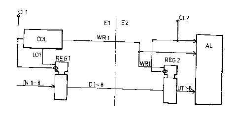
Figure 2 illustrates the interFace units E1 and E2 in the form of a block
dia(Jrarn. ~ register REG 1 on the transmitter sid~ is built up from 8 flip-flops
which can be fed with an 8-bit inforn-lation word via the inputs IN 1-8 when a
feed signal LO1 simultaneously occurs with the receding flsnk of the clock
signal CL1 on the inputs of the register flip--flops. A control logic COL drivenby the clock pulses CL1 has the task of
a) generating the feed signal LO1 -for writing the information word into the
register REG1,
b) yenerating a write signal WR1, which is fed via the interface to the receiverside for writing into a register REG2 the data word transferred in parallel on
the lines D1-D8. The binary values from REG 2 are transmitted to a logic AL
which converts parallel data to series data for further transmission to the PCM
system.
The conditions are illustrated by the pulse diagrams 3a-3h, where Figure 3a
illustrates the clock pulses CL1 on the transmitter side and 3b illustrates the
feed pulse LO1. When the feed pulse LO1 occurs simultaneously as the receding
flank o-f the clock pulse CL1, the binary values occuring on the inputs IN1-8 onthe register REG1 are written into the register flip-flops. These values then
occur on the lines D1-8 so that the previous value on the flip-flop outputs is
2û changing according to Figure 3c. The write signal WR1 in Figure 3d simulta-
neously occurs on the output o-f the control logic COL and i5 led to the receiver
side E2. The receiver register REG2 obtains the write signal WR1 (Figure 3d)
from the transmitter side as well as the clock signal CL2 (Figure 3e~ from the
receiver side and the lenght of the write signal WR1 is selected such that the
receding flank of the clock signal will occur before the write signal WR1
ceases. In this way, when the receding flank of the clock signal CL2 occurs the
binary values from REG1 are transferred to REG2 via the lines Dl-8, and these
values will Gccur on the REG2 outputs Ut 1-8 for further passage to the logic
AL.
This arrangement allows there to be no alteration of the clock pulse CL2. If it
should be necessary to change the clock period for some reason, e.g. to double
the length as illustrated in Figure 3, the transmission cannot be carried out,
since the write pulse WR1 would ceas~3 before ~he receding flank in the twice sslong clock pulse occurs (Figure 39). No change of state on the outputs D1-8
7~9
would be received (Figure 3h) by REG2 to occur on the outputs Ul-U8 of the
latter on occurrence of the receding flank of the clock signal CL2. The only
possibility is thus to alter the length of the write pulse WRl, which cannot be
done without necessary structural alterations to the transmitter side. The
object of tha invention is to enable alteration of the receiver side clock period
without any structural alteration on the transmitter side.
Figure 4 illustrates the inventive solution, the apparatus shown containing, in
the same way as the apparatus according to Figure 2, a reigster REGl on the
transmitter side El and a register REG2 on the receiver side E2, the registers
being in communication with each other via an 8-wire line and are controlled by
their individual clock signals CLl and CL2. The write signal which will o~cur onthe receiver side will be dependent on the write signal on the transmitter side
and also~ on the receiver side clock signal. The outputs C) l~~ of REGl are
actuated in the same way as for the apparatus accorcling to Figure 2, ancl theirbinary values are altered by the feed signal LOl occuring simultaneously with
the receding flank (Figures 5a,5b) of the clock signal CLl. A state signal WRl
occurs on the a output of a first J-K flip-flop Fl (Figure 5c). The condition for
transmitting to REG2 is that both a write signal and the receding flank of the
clock signal CL2 occur simultaneously. In accordance with the invention9 the
length oF this write signal WR2 is independent of the transmission side clock
signal CLl, and is solely determined by the receiver side clock with the aid of a
logical circuit~ This logical circuit comprises in accordance with the embodi-
ment a D flip-flop D2, an EXCLUSIVE-OR circuit X2 and a JK-flip-flop F2.
When no transmission takes place the outputs of all these flip-flops have
identical values, which is the one of two possible values. When there has been achange in state on the Q output of the Fl flip-flop, i.e. it has assumed a second
alternative value, this signifies that the state signal WRl is fed to the D flip-
flop D2, which obtains the same state on its Q output (Figure 5f) on the
occurence of the receding flank of the clock pulse CL2. As soon as this change
in state has occured, the output signal WR2 (Figure 5h) of the EXCLUSIVE-OR
circuit X2 is changed when the input signals to the circuit X2 are instantly
different (figures 5F, 59). For the next subsequent receding flank of the clock
signal CL2 the binary values are transmitted on the lines Dl-8 to REC:2 and
occur on the outputs UT-8 of REG2 and the value on the Q output of the circuit
F2 is changed, whereby the signals on the X2 circuit inputs once again become
3t~3
the same, 1l1cl consequently the signal WR2 ceases from the circuit X2. In thisway the write signal WR2 has been interrupted and the state of the outputs on
the circuits Fl, D2, X2 and F2 are once again identical. rhis means that REG2
is ready for reception of the next inFormation word, which is started by a new
char-ge of state on the Q output of the circuit Fl. If it is desired to alter the
receiver side clock period, e.g. to make an extension thereof, no structural
alteration to the sender side is required, and the write pulse WR2 will be
automatically adjusted to the period length of the clock signal CL2. This is
illustrated in the right hand part of F igure ~ where the clock pulse has been
extended. As will be seen, the period length o-F the signals CL2 will in this case
regulate the length of the write pulse WR2 in a manner such that the write
pulse WR2 opens the flip-Flops of the register REG2 for reception of binary
information via the wires Dl-D8 when the receding flank o-F the clock pulse CL2
occurs. In this way there is complete independence of the relationship between
the period lengths o~ the two clocks, and only the period time of the clock
signal CL2 will determine the minimum time necessary for transferring
information from the transmitter side to the receiver side.