Note: Descriptions are shown in the official language in which they were submitted.
73 3
ELECTRON BEAM DIRECT DRAWING DEVICE
BACKGROUND OF THE INVENTION
The present invention relates to a direct drawing
device for drawing a predetermined pattern on a photoresist
layer on a printed circuit board by scanning it directly with
electron beam.
A substrate patterning technique has been used in
manufacturing semiconductor device or printed circuit board
in which an art work film bearing thereon a predetermined
pattern is put on a photoresist layer formed on the semicon- -
ductor substrate or the printed circuit board, which is
sensitive to ultra-violet ray, and exposed to ultra-violet
ray and a copper foil pattern, i~e., bare board, is formed
after developing and etching thereof. The art work film is
usually prepared by a drawing machine called photo plotter
or laser plotter. A drawing pattern data which is given by a
computer aided printed circuit board design is supplied to
the plotter in which it is converted into a data of a suit-
able format which is referred to as "Gerber Format" which is
composed of a code corresponding to a line width of a pattern
20 and a code assigning a start point cordinate (Xs, Ys) and
an end point coordinate (Xe, Ye) of each line segment there-
of and a code showing whether or not these line segments are
to be exposed and represents a group of patterns over a large
. . .
circuit board area such as 340 mm X 400 mm or 500 mm X 600 mm.
Recently, in order to eliminate the necessity of
preparation of the art work film and to reduce a manufactur-
ing cost and time as well as to match ~ith a requirement of
production of various semiconductor devices or printed circuit
boards each small in number, an electron beam direct exposing
system has been developed, in which a predetermined pattern is
drawn on a semiconductor wafer or a mask plate by scanning it
with el~ctron beam. In order to make such direct exposing
system usable with the conventional plotter, it is desired that
the direct exposing system is responsible to the computer aided
design (CAD) output pattern information of the Gerber Format
and able to convert it into a suitable format to the system.
In the direct exposing system, when a large area
15 is to be drawn by scanning it with electron beam while the
area is kept stationary, a peripheral portion of the field
is irradiatéd with electron beam at a small incident angle
causing positions of exposition at an upper and a lower
surfaces of the phoresist layer to be different, resulting
20 in a degradation of positional accuracy of a resultant pattern.
In order to solve this problem, it is considered to make a
work distance between the circuit board and a deflector large
enough to obtain a sufficiently large incident angle of
electron beam. In this case, however, it becomes difficult
25 to condense electron beam and the latter may be scattered by
-- 3 --
residual gas and thus influenced by residual magnetism due
to a long beam path. Therefore, the area ~o be scanned by
electron beam should be limited to, for example,
100 mm X 100 mm which can be scanned by a main deflector,
i.e., main deflection regions (referred to as "field",
hereinafter), and the respective fields are drawn by the so-
called "step and repeat" system one by one by relatively
moving the field with respect to electron beam. Therefore,
it is necessary that a pattern data over the whole area is
divided every field and then edited again. It ~as been usual
to divide a region which can be covered by electron beam
deflected by a main deflector into a plurality of sub-
deflection regions (referred to as "sub-~ield", hereina~ter)
each covered by a sub-deflector and to shift electron b~am
from one sub-field to another by the main deflector every
time a drawing for the one sub-field completes to thereby
complete a drawing of the whole field.
This system is disclosed in, for example, Japanese
Patent Application Laid-open No. 244024/19~5 and Fig. 4 of
the present application shows a portion of a conventional
electron beam exposing device having a two-step deflector
disclosed therein.
In Fig. 5, electron beam 1 is directed through a
blanker 2, an aperture 3, a sub-deflector 4 and a main
2~ deflector 5 to a material 6 such as a semiconductor wafer
7~'~
~,
or a mask plate thereon. A region of the material 6 surroun-
ded by a solid line is a field and regions thereof surrounded
by dotted lines are sub-fieldsO A control circuit for contro-
lling the electrooptical system mentioned above is also shown
in block in Fig. 4 in which a computer 7 is connected through
a drawing data memory 8, a pattern decomposer circuit 9, a
sub-deflection correcting circuit 10 for correcting distors-
ion of sub-deflection, a dot decomposer circuit 11 for a small
region and a sub-deflection digital/analog converter (DAC)
12 to the sub-deflector 4 and through a correction coefficient
calculator circuit 13 and a main deflector DAC 14 to the main
deflector 5. The sub-deflection correction circuit 10 is
connected to the correction coefficient calculation circuit 13
and through a blanking amplifier 15 to the blanker 2.
Fig. 6 illustrates an example of drawing operation
to be performed by the conventional electron beam exposing
device. A left side portion of Fig. 5 shows the material 6
and a right side portion thereof shows one (22) of the sub-
fields in the field 21 in enlarged scale. A pattern 23 in the
~ sub-field 22, such as trapezoidal pattern, is divided into
seven small regions ( paint-out fields). One (24) of the paint-
out fields is painted out digitally in dot by point electron
beam 1.
In operation, a deflection of electron beam 1 from
one sub-field to another is performed by the main deflector
~ ~r71~3~73~
-- 5
5 and a deflection thereof withln each sub-field is performed
by the sub-deflector 4. The computer 7 supplies a drawing
data to the drawing data memory 8 and a deflection distorsion
data to the correction coefficient calculator circuit 13.
One of outputs of the calculator circuit 13, which assigns a
center of the sub-field in the field after correction of its
deflection distorsion, is supplied to the main deflector DAC
14. The pattern decomposition circuit 9 divides the pattern
in the sub-field into the paint-out regions on the basis of
the pattern data received from the drawing data memory 8.
The sub-deflection correcting circuit 10 receives another
output of the correction coefficient calculator circuit 13
which is a deflection correcting coefficient for each sub-
field and performs a distorsion correction according thereto~
a resultant corrected sub-deflection signal being supplied
to the dot decomposer circuit 11 in which each paint-out
field is decomposed to dots which are supplied to the sub-
deflection DAC 12.
The blanking amplifier 15 responds to the output
of the sub-deflection correcting circuit 10 to perform a
blanking operation at both a start point and an end point
of the paint-out field so that electron beam 1 is on-off
controlled thereby.
The drawing data memory 8 stores pattern informa-
tions of the respective sub-fields of the field which are
7~
prepared by the computer 7 by dividing the field.
As mentioned previously, this proposal requires
the division of the pattern data of the large area into
those of the fields and the re-edition thereof and additiona-
lly the division of pattern data of each field into thoseof the sub-fields and the re-edition thereof. When these
operations are to be performed by a computer, the amount of
software necessary to the divisions and the re-editions
becomes considerable and the amounts of data and processing
~ime becomè also considerable, respectively. When it should
be performed by a hardware, it is necessary to provide a
circuit for a~tomatically dividing the field patern data
to the respective sub-field pattern data. Thus, in either
case, the processing of the data becomes complicated and
time consuming. Further, unlike the wafer or mask pattern
for semiconductor device, it is usual that the pattern of
printed circuit board does not include identical pattern
portions occuring repeatedly. Therefore, it is impossible
to simplify the data processing by using features of such
repeatedly occuring idential pattern portions.
SUMMARY OF THE INVENTION
An object of the present invention is to provide
an electron beam direct drawing device which is capable of
drawing a data pattern highly precisely through a through-put
process including a data processing on the basis of output
: ' ' '
pattern data of the C~D in such a way that, in scanning and
exposing a printed circuit board having large area with
electron beam, drawing pattern data of a field which are
divided and then re-edited complete a drawing of the pattern
without necessity of a further division to sub-fields.
Another object of the present invention is to
provide an electron beam direct drawing device which is
capable of providing a high quality drawing on a printed
circuit board by controlling a dose of electron beam to an
optimum value regardless of variation of width of pattern
to be drawn so that an optimum exposure is always obtained.
According to a first aspect of the present invention,
the above objects can be achieved by an electron beam direct
drawing device comprising means for dividing a CAD output
drawing pattern information over a whole axea of a printed
circuit board into a plurality of fields and for re-editing
drawing patterns of the respective fields, means for storing
the divided and then re-edited drawing pattern information,
means for reading out the stored drawing pattern information
sequentially and performing a main deflection of electron
beam by means of a main deflector and means for deriving,
from the stored drawing pattern information, information
assigning an orientation of a pattern to be drawn and a scan
width of a sub-deflection and for performing a predetermined
2~ sub-deflection scanning by means of a sub-deflector.
S3~73~
According to a second aspect of the present inven-
tion, the above objects can be achieved by providing an elec-
tron beam direct drawing device comprising means for storing a
drawing pattern information corresponding to a field capable
of being scanned by a main deflector, means for reading out
the stored drawing pattern information sequentially and
performing a main deflection of electron beam by means of a
main deflector, means for producing a plurality of signals
having rectangular waveforms and having different frequPncies,
means for deriving, from the stored drawing pattern inormat-
ion, an information assigning a width of sub-deflection scan
and for selecting one of the rectangular signals, means for
producing a main deflection scanning data in synchronism
with the selected rectangular signal and means for deriving,
from the stored drawing pattern information, information
assigning an orientation of a pattern to be drawn and a scan
width of a sub-deflection and for performing a predetermined
sub-deflection scanning by means of a sub-deflector.
In the present invention, pattern drawings of respect-
ive fields which once divided and re-edited are performed at
high speed in each interval between main deflection scannings
in real time as patterns having a predetermined width without
necessity of sub-division thereof. Further, dose of electron
beam is always controlled to an optimum value even if the
pattern width is varied, realizing an optimum exposure for
i,
~'7~973~
_ 9 _
various patterns in the fields.
BRIEF DESCRIPTION OF THE DRAWINGS
Fig. I is a block diagram of an embodiment of the
present invention;
Fig. 2 is a block diagram showing a sub-deflection
control circuit in Fig. 1 in more detail;
Fig. 3 shows waveforms and graphs useful to under- -
stand an oper~tion of the sub-deflection control circuit;
Fig. 9 is a block diagram of another embodiment of
the present invention;
Fig. 5 is a block diagram showing a conventional
device; and
Fig. 6 shows a field in FigO 5 in enlarged view.
DETAILEl:) DESCRIPTION OF THE PREFERRED E BODIMENTS
lS In Fig. 1 which shows an embodiment of an electron
beam direct drawing device according to the present invention,
an electrooptical system composed of a blanker 2, an aper-
ture 3, a sub-deflector 4 and a main deflector 5 is substan-
tially the same as that shown in Fig. 5 and disposed in a
reduced pressure environment. Therefore, details thereof are
omitted in this description for avoidance of duplication.
However, the sub-deflector 4 of this embodiment is constitu-
ted with a deflection coil 4-1 for scanning in X direction
and a deflection coil 4-2 for Y direction scanning and the
main deflector 5 of this embodiment is constituted with an X
:
.. . ...
, ~
9~
-- 10 --
direction scanning coil 5-1 and a Y direction scanning coil
5-2. Electron beam 1 passed through the electrooptical system
impinges a printed circuit board substrate 31 having a photo-
resist thereon. The substrate 31 is supported on a XY table
32 which is driven in X and Y directions according to
instructions from a table control system 33. The XY table 32
having the substrate 31 thereon is disposed in reduced pres-
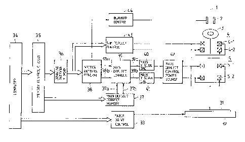
sure environment. The drawing device is composed of a computer
34, a memory control circuit 35 connected to an output side
of the computer 34, a drawing pattern memory 36 connected
to an output of the memory control circuit 35, a main deflec-
tion correcting memory 37 connected to the output Gf the
memor~ control circuit 35 and storing distorsion correct-
ing data for correcting distorsion of deflection usually
existing in the electrooptical system, a vector pattern
generator circuit 38 responsive to a pattern data from the
drawing pattern memory 36 to generate deflection scanning
data, a main deflection correcting circuit 39 responsive to
the deflection scanning data from the vector pattern genera-
tor circuit 38 and the distorsion correcting data from themain deflection correcting memory 37 to generate a corrected
deflection scanning data, a main deflection X scan DAC 40
connected to an output of the main deflection correcting
circuit 39, a main deflection Y scan DAC 41 connected to
the output of the main deflection correcting circuit 39, a
3~3 ~
-- 11 --
main deflection control power source 42 for supplying control
power to the main deflection X and Y scan DACs 40 and 41 and
the X and Y main deflection coils 5-1 and 5-2, a sub-
deflection control circuit 43 connected between the drawing
pattern memory 36 and the sub-deflector 4 and a blanker
control circuit 44 connected between the vector pattern
generating circuit 3~ and the blanker 2 for on-off controll-
ing the electron beam 1 at start/end times of drawing for
each field.
- lO Fig. 2 is a block circuit diagram of the sub-
deflection control circuit 43 in Fig. 1. The sub-deflection
control circuit 43 includes a periodic rectangular ~aveform
generating circuit 45 whose output signal 45a is supplied,
directly, to a X scan gain generator circuit 96 and to a
phase signal selection circuit 48 to which a signal 45b which
is obtained by inverting the signal 45a by an inverter 47 is
also supplied. The phase signal selection circuit 4B func-
ions to select either the signal 45a or 45b according to a
digital input value supplied from the drawing pattern memory
36 and supplies a selected signal to a Y scan gain generating
circuit 49. The X scan gain generating circuit 46 is composed
of a plurality of amplifiers 46a, 46b,..46i and the Y scan
gain generating circuit 49 is composed of the same number of
amplifiers 49a, 49b, .49i. The amplifiers 46a and 49a amplify
original signal na times, the amplifier 46b and 99b amplifv
~'7~
- l2 -
1 it nb times, and so on. na, nb,... ,ni are set preliminarily
such that a sub-deflection scanning of a predetermined width
can be performed on the substrate 31, respectively. Since
the pattern width takes discrete values such as 70 um for
S ultra X class, 130 um for X class and 250 um for Y class,
the number of the amplifiers having preset multiplication
factors ls not infinite.
An X scan gain selection circuit 50 responds to a
pattern data from the drawing pattern memory 36 and selects
one of outputs of the amplifiers 46a to 46i and A Y scan
gain selection circuit 51 responds thereto and selects one
of outp~ts of the amplifiers 49a to 49i.
In operation, an output (drawing pattern informat
ion of Gerber format) of a printed circuit board pattern
design CAD (not shown) is supplied through an on-line
communication line or a magnetic tape, etc., to the computer
34 in which it is divided to drawing pattern informations
for respective fields. This process of converting the
pattern data into information for the various fields is
~n referred to as "re-editing". This re-edited data is
converted into binary data (referred to as "direct drawing
pattern information, hereinafter) suitable for use in the
direct drawing device. The direct drawing pattern
information includes binary digital values of, for example,
2S a coordinates (X,Y) of the start point of drawing, length of
line segment, orientation and sub-deflection gain
information for each line segment of the drawing pattern.
;3~
- 13 -
Prior to a commencement of the drawing operation,
the direct drawing pattern information and the main deflection
correcting data are supplied by the computer 34 through the
memory control circuit 35 to the drawing pattern memory 36
and the main deflection correcting memory 37 and stored there-
in. At the start of the direct drawing, data concerning to a
start point (X, Y) coordinates, length and orientation of one
line segment are readout from the drawing pattern memory 3~
and supplied to the vector pattern generating circuit 38. The
latter circuit is constituted with an electronic logic circuit
such as counter and provides an X scan data 38a and a Y scan
data 38b in digital form as X and Y scan control signals for
the main deflector 5 in response to the above mentioned three
data. The scan data 3a and 38b are supplied to the main
deflection correction memory 39 in which a main deflection
correcting operation is performed in real time according to
the correction data from the main deflection correction memory
37, i.e., an X scan correction data 37a and a Y scan correction
data 37b, and, after the correction is completed, supplied to
the main deflection X and Y scan DACs 40 and 41 as a corrected
X scan data 39a and corrected Y scan data 39b, respectively.
The corrected X and Y scan data 39a and 39b are con~erted by
the respective DACs 40 and 41 into analog signals which are
supplied to the main deflection control power source 42, upon
25 which the latter supplies certain currents to the main deflec-
.
"3 ~
- 19 -
tion X and Y coils 5-1 and 5-2 to perform the main deflection
scanning.
When the main deflection scanning for the one line
segment is completed, data for a next line segment are read-
out from the drawing pattern memory 36 and the same operationis repeated for the next line segment, and so on. Thus, a pre-
determined drawing can be performed on the basis of the pattern
in the field.
The sub-deflection scanning will be described in
detail with respect to Fig. 2. In Fig. 2, when the X sub-
deflection coil 4-1 and the Y sub-deflection coil 4-2 are
supplied with such rectangular in-phase oltages VFx and ~y
having amplitudes ~H and VyH as shown in Figs. 3a and 3b,
respectively, current variations ix and iy having ampli-
tudes iXH and ~H shown by dotted lines in the same figuresare produced in the sub-deflection coils 4-1 and 4-2,
respectively. In this case, the following relations are
established between a sub-deflection direction ~ and deflection
width Lxy of electron beam 1 on the substrate 31:
~ = tan ( V ) = tan (1
XH XH
X XY cos 9 = KVXH = K' ix~
Ly = Lxy-sin ~ = KVyH = K' iYH
where K and K' are constant and I'X and Ly are an X and a Y
components of the deflection width L~y .
Fig. 3c shows a movement of electron beam 1 on the
3'~
- 15 -
substrate 31. Since the rectangular vol~ages VFX and VFY are
in phase, electron beam 1 moves in the first and the third
quadrants as shown. When the voltages VFx and VFy are different
in phase by 180 as shown in Figs. 3d and 3e, electron beam 1
moves in the second and the fourth quadrants as shown in Fig.
3f. Chain lines in Figs. 3c and 3f show the main deflection
scan direction.
An operation of the sub-deflection control circuit
43 will be described. Orientation and sub-deflection gain
information among other data for one line segment of a patt-
ern readout from the drawing pattern memory 36 are supplied
to the ~ scan gain selection circuit 50 and the Y scan gain
selection circuit 51. It is assumed at this time that the main
delection scannin~ is performed in a direction parallel to
the X axis according to data of a start point coordinates
(X, Y), length and orientation of one line segment readout
from the drawing pattern memory 36, as an example. That is,
= 0 or 180 in Figs. 3c and 3f. In such case, the X scan
gain selection circuit 50 selects an output of the amplifer
46a, i.e., the signal 45a, and the Y scan gain selection
circuit 51 selects an output of the amplifier 49i. As a
result, no sub-deflection amplitude is given to the X scan
coil 4-1 and a rectangular voltage having magnitude ni times
that of the original signal is given to the Y sub-deflection
coil 4-2 to give a predetermined deflection in a direction (Y
7~3t7;3
- 16
axis direction) orthogonal to the main deflection direction
(~ axis direction).
When the main scanning is being performed in the Y
axis direction ( ~ = 90 or 270~, the X and Y scan gain
selection circuits 50 and 51 select outputs of the amplifiers
46i and 49a, respectively, to give a predet~rmined sub-
deflection in a dixection (X axis direction) orthogonal to the
direction of the main deflection~
When the phase signal selection circuit 48 selects
in-phase rèctangular signals and the X and Y scan gain select-
ion circuits 50 and 51 select the outputs of the amplifiers
4~b and 49i, respectively, a sub-deflection scanning satisfy-
ing
~ = tan 1 n ( ~ 9 ~ 90 ~ is obtained and, when the cir-
lS cuit 48 select rectangular signals opposite in phase, a sub-
deflection satisfying a = tan n ( 90< ~'< 180 ~ is obtained.
Thus, it is possible to sub-scan in a direction normal to the
main deflection in any direction other than vertical or
horizontal direction.
Fig. 4 shows another embodiment of the present
invention which differs from the embodiment shown in Fig. 1
in only that an optimum electron dose control circuit is
further included. The optimum dose control circuit comprises
a clock circuit 28 for generating a rectangular clock signal
having a constant frequency fM , a frequency divider 29 for
,
- 1 7 ~ 9~73~
frequency dividing the clock signal to produce rectangular
signals having frequencies fa ~ fb ~ ~ fi on signal lines
23a, 29b,..,29i and a clock selection circuit 30 ~or select-
ing one of the frequencies fa to fi . The frequency selected
by the clock selection circuit 30 is supplied to a vector
pattern generating circuit 38 which is the same as that shown
in Fig. 1 and used as a reference timing clock signal for
generation of the main scan data. The optimum dose control
circuit functions to control electron beam dose to an optimum
value even if the width of pattern line varies, so that an
optimum exposure is always obtained to improve the quality of
drawing. Since a construction of other portion of this embod-
iment than the optimum dose control circuit and an operation
thereof are the same as those of the ~mbodiment shown in Fig.
1, an operation of the latter circuit will be described.
In Fig. 4, among the data readout from the drawing
pattern memory 36, the sub-deflection gain information in
digital form is also supplied to the clock selection circuit
30, upon which the latter circuit 30 selects one of the
frequencies fa to fi as a main scan control clock fM so as
to keep the exposing dose constant with respect to the patt-
ern width to be drawn, i.e., scan width d of sub-scan, and
supplies it to the vector pattern generating circuit 38.
A scan area S (m~) which can be scanned by sub-
deflection within a time tM (sec) necessary to move the main
73~
deflection beam in response to a variation of main deflectionscan corresponding to one bit of digital data is expressed by
the following equation;
S =~ d ........................... (1
where ~ is a beam spot diameter in meter.
On the other hand, there is an optimum amount of
charge, i.e., dose D (Coulomb/m2), to expose a unit area of
the photoresist, which can be expressed by
D = (I tM )/S .................... (2)
where I is electron beam current in ampere.
Therefore, the following relation is obtained from the equa-
tions (1) and (2)
tM = ( ~-D) d/I ................... .(3)
Since tM = 1/fM ~ the equation (3) can be transformed into
the following equation by controlling tM by clock frequency
fM (Hz~
fM = (l/(~ D))-(I/d) ............. (4)
This means that, in order to control the dose D always optimum
according to the sub-scan width d while the beam current I is
kept constant, it is necessary to change the main scan control
clock.
Also, from the equation (~), it is clear that the
dose D can be kept constant with respect to variation of the
sub-scan width by controlling the beam current I while keep-
ing the clock frequency fM constant. However, the drawing
- ~ .
- 1 9 ~ ~7~3~73~
under control of the beam current provides problems such as
(1) It is necessary for wide pattern line to use an
electron tube ha~ing a cathode of a diameter large enough to
derive a large beam current and such larger cathode causes
beam condensation to be degraded.
(2) When the beam current is controlled by controlling
a grid voltage of the electron tube, a focus point may fluc-
tuate due to a large variation of field distribution around
the cathode.
(3) In a case where the current is controlled by
controlling a filament current of the tube to control cathode
temperature, the control response becomes as low as the order
of 1 sec.
The present control system in which the main scan
lS speed is variable while the beam current is kept constant is
free from the above mentioned problems.
Since, as is clear from the equation (4), the main
scan clock frequencies fa to fi for obtaining optimum dose for
respective sub-scan width da to di can be determined directly,
it becomes possible to obtain an optimum exposure for each of
pattern widths by selecting one of these frequencies according
to a drawing data.