Note: Descriptions are shown in the official language in which they were submitted.
~l~7g'~33
DIGK:014
OUTER TAPE AUTOMATED ~ONDING
SEMICONDUCTOR PACKAGE
Thi~ invention relates generally to the field of
packaging for integrated circuit chips, and more
particularly to tape automated bonding packaginy.
Packaging is one of the final steps in the process of
manufacturing integrated semiconductor circuit components
or chips. In packaging, a fabricated semiconductor chip
is mounted in a protective housing. After packaging, the
assembled component is subjected to final testing and then
connected to an electronic circuit.
Currently, many semiconductor chips are contained in
plastic packages. These packages are provided with
reinforced metal leads for electrically connecting the
chip to the printed circuit board which contains the
circuit in which the chip is to be included. Within the
package, one end of each lead is connected to a specific
bonding point on the chip, usually by an intermediate
lead; the other end of the lead, which extends outside of
the package, is attached to a connection on the printing
circuit board.
-2- ~ 73`~
Recently, advances in semiconductor manufacturing
technology have made the fabrication of Very Large Scale
Integration (VLSI) chips possible. VLSI chips comprise a
large number of individual circuit components that are
fabricated together on a single~ very small chip. VLSI
chips are able to perform a large number of electrical
functions, and perform them more rapidly, then was
previously possible.
To date, it has been difficult to provide suitable
packaging for VLSI chips. In part, this is because each
chip requires a large number of connections to external
circuit elements. Many VLSI chips have 100 to over 300
bonding points each of which must be connected to a lead
for connection to external circuit elements.
Another consideration in the use of a VLSI chip i5
the need to provide common voltages to a number of
different locations on the chip~ For instance, a chip
that comprises a number of individual transistors, such as
C-MQS type transistors, may require a common drain voltage
supplied by an external power supply that is applied to
the drain terminals of all the transistors, and a common
source voltage also provided by an external power supply
applied to the source terminals of all the transistors.
Typically the drain voltage is positive with respect to a
common reference or ground voltage, and the source voltage
is typically at the same level as the ground voltage. The
common voltages need to be supplied to the chip so the
individual components all operate with respect to a common
power level. Normally, common voltages are supplied to
the components on the chip by providing sets of leads,
each set designed to carry the same voltage, to different
bond points on the chip.
- 35
3t733
Providing a VLSI chip with a common voltage at a
number of locations has, to date, been a difficult task.
In a VLSI package, the leads which are connected to the
chip are spaced closely together. Moreover, some of the
leads supply voltages such as signal voltages that
fluctuate rapidly as electronic functions are performed on
them by the chip and the other circuit components. This
causes the magnetic field normally developed around these
leads to vary, whlch in turn causes an inductive current
to Elow in adjacent leads. Whenever a sufficiently large
inductive current is developed in a common voltage lead,
the voltage it is carrying changes. This problem may be
intensified because in a V~SI chip such as a digital logic
chipj voltages may fluctuate rapidly; this rapid change
intensifies the development of a magnetic field and the
associated inductive current flow. As a result, the
voltage supplied to one or more components on the VLSI
- chip may vary so greatly as to cause the chip to
malfunction.
There have been some attempts at providing packages
for VLSI chips that are designed to minimize the problems
associated with the development of inductive current flow.
One such package is a multi-layered ceramic package. This
package includes layers of conductors separated by layers
of dielectric ceramic that are pressed together. A cavity
is formed in the layers, and the chip is mounted in the
cavity. Wire bonds are used to connect the bond points on
the chip to the individual conductors on the top layer of
conductors. Individual wire bonds or reinforced metal
leads are used to provide an electrical connection to the
printed circuit board the chip is attached to. Selected
top-layer conductors, which carry common voltages, are
connected to common intermediate-layer conductors. The
intermediate-layer conductors function as reference
voltage planes which insure the common voltages supplied
-4- ~79~733
through the top-layer conductors attached thereto does not
appreciably vary.
However, there are a number of limitations associated
with mul~i-layer ceramic packages. The size of these
packages tends to be extremely large in order to
accommodate the interconnections needed between the
conductor layers. Moreover, a multi-layered ceramic
package designed to contain a VLSI chip is expensive to
manufacture. In some instances, the cost of the multi-
layered ceramic package may significantly exceed the cost
of fabricating the chip.
`The invention provides a new and improved
semiconductor chip package that occupies a minimal amount
of space, is easy to assemble, and economic to
manufacture, and which minimizes inductive voltages that
can disrupt the voltage over the common power supply leads
in the semiconductor chip assembly.
In brief summary, the new package includes a housing
for a chip bonded to a frame of TAB (Tape Automated
Bonding) tapeO The TAB tape comprises an insulating film
which supports a number of conductive leads formed on it.
The TAB tape includes a center opening where the chip is
to be located. Each conductive lead has an inner portion
which projects into the center opening and is attached to
a bond point on the chip; and an outer portion which
projects beyond the outer perimeter of the film and is
attached to a contact on the printed circuit board. The
housing covers the chip and a small portion of the TAB
tape inner lead portions.
A layer of conductive film is attached to the surface
of the TAB tape opposite the leads. The conductive film
subtends an area around the TAB tape. Vias electrically
5--
7~3
connect the leads on the TAB tape that provide a common
voltage to the components on the chip.
An advantage of this semiconductor package is that it
connects directly to the external circuitry without the
use of an additional level of reinforced leads between the
chip and the external circuitry. This eliminates the need
to provide a large package for the chip that would obviate
the advantage gained by miniaturization. Moreover, this
significantly reduces the complexity of providing the chip
package, and substantially reduces the cost of its
manufacture.
The conductive film serves as a reference plane for
the common voltage such as a ground voltage. Since the
common voltage leads each are connected to the conductive
layer, the voltage across each lead to their respective
bond points on the chip are identical. In other words,
the conductive film minimizes the affect of inductive
~0 voltage flux in the common voltage leads so each such lead
provides a constant common voltage to the chip component
it is connected to.
This invention is pointed out with particularity in
the appended claims. The above and further advantages of
this invention may be better understood by re~erring to
the following description taken in conjunction with the
accompanying drawings, in which:
Figure 1 is a perspective view of a TAB semiconductor
package of this invention attached to a printed circuit
board containing an electronic circuit.
Figure 2 is an exploded view, from the base of the
housing, showing the disassembled TAB semiconductor
components of this invention.
-6~ 7t~3
Figure 3 is a cross-section view of the TAB
semiconductor package of thi.s invention.
Figure 4 is a perspective view of an alternative
embodiment of the TAB semiconductor package of this
invention.
Figure 5 is a top view of an alternative embodiment
of metal film used with the ~AB semiconductor package of
this invention.
Figure 1 illustrates a Tape Automated Bonding (TAB)
semiconductor package 10, constructed in accordance with
this invention, attached to a printed circuit board 12.
Adjacent the TAB semiconductor package 10 are conventional
plastic semiconductor packa~es 14 and other components 16
that are part of the electronic circuit assembled on the
printed circuit board 12.
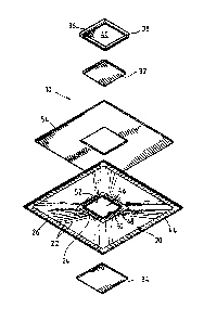
Referring to Figures 2 and 3, the TAB semiconductor
package 10 of this invention is shown in greater detail.
The TAB semiconductor package 10 includes a housing 18,
containing a semiconductor chip 32, which is attached to a
section of TAB tap~ 20 that surrounds the housing. The
chip 32 and housing 18 subassembly is housed in a center
opening 46 formed in the TAB tape 20~ A number of
conductive leads 22 are plated on the surface of the TAB
tape 20. Each lead 22 has an inner lead portion 24 that
extends into the center opening 46 and is attached to a
bond point on the chip within the housing 18, and an outer
lead portion 26 attached to a contact pad 28 on the
printed circuit board. The contact pads 28 are connected
to conductors 30 on the printed circuit board 12 to
electrically connect the chip to the appropriate external
circuit component~.
7~733
~6382-33
The chip 3? iS eontained lnside the housing 1~ formed of
plas~i~ or ceramic which comprises a base 34 on which the chip is
seated and a cover 36 which extends over the base and dPfines a
space 40 larye enougn so the chip may be housed therein. The
cover 36 includes rim 38 which defines the perimeter of space 40.
The leads 22 are formed on the 'PAB tape 20 according to
standard TAB practice. The TAB tape may be a film 42 of polymide,
Kapton, or other suitable insulating dielec~ric.
The outer leads 26 each extend out irom the outer
perimeter of the TAB film 42. An outer support ring 44, also
formed of polymide, is spaced away from the TAB fil~ 42, and is
secured over the ends of the outer lead portions 26. The outer
suppor~ ring 44 secures the outer lead sections 26 so they do not
curl or cross, or o~herwise become out of registration with the
contact pads 28 during bonding thereto.
The inner lead portions 24 each extend into the center
lead opening 46 perpendicularly wi~h respec~ to the inner
perimeter of the TAB film 42. An lnner support ring 48 that is
spaced interiorly away from the inner perimeter of the TAB film 42
prevents the inner lead portions 24 from curlingr crossing or
otherwise becoming out o~ registration. The inner lead portions
extend inwardly from the inner support ring 48 to provide end
sections 52.
'
-8 ~ 33
The TAB tape 42, inner support ring 48 and inner lead
portions 28 are dimensioned to provide film~free sections
50 of the inner lead portions 24 approximately equal to
the width of the rim 38 of cover 36 The chip 32, rim 38,
space 40, and inner support ring 48 are dimensioned so the
chip is centered in the space and there is sufficient area
between the chip and the rim to accommodate the inner
support ring.
A layer 54 of conductive metal film is bonded to the
underside of the TAB film 42. The metal film layer 54
extends completely underneath all of the TAB film 42, and
may also extend under the outer support ring 44 and the
inner support ring 48. Vias 56 extend through the T~B
film 42 to electrically connect selected leads 22a to the
metal film 54. In one specific embodiment of this
invention, the leads 22a that are connected to the metal
film 54 are connected by a plurality of vias 56 that are
spaced apart from each other.
The TAB semiconductor package 10 of this invention is
assembled by first bonding the chip 32 to the TAB tape 20
in accordance with standard tape automated bonding
practice. The chip 32 is bonded to the ~AB tape 20 inside
the center opening 46 and within the area defined by the
inner perimeter of the inner support ring 48; the inner
lead's end sections 52 are connected to bond points on the
chip 32.
After tape bonding, the chip 32 is enclosed within
the protective housing 18. The base 34 is placed under
the chip 32 and the cover 36 placed over the base. Epoxy,
or other suitable adhesive, is used to seal the cover 36
and base together at the top surface of cover rim 38. The
tape bonded chip subassembly is positioned so the TAB film
and conductive film-free sections 50 of the inner leads 24
~,7~3~
are positioned between the rim 38 and the cover 36 and the
adhesive is applied between them.
The TAB semiconductor package 10 may be assembled by
automated equipment. The TAB tape 20 may be provided with
conventional excisable test pads (not illustrated), for
testing of the assembled package 10. After assembly and
testing, the TAB semiconductor package may be installed on
the printed circuit board 12. As seen in Figure 3/ the
package 10 is mounted on the printed circuit board so the
base 34 of the housing 18 and the leads are adjacent the
printed circuit board 12, and the cover 36 of the housing
and the metal film 54 are exposed. The outer leads 26 may
then`be attached to the printed circuit board contact pads
28`.
The TAB semiconductor package 10 protects the chip
32. Furthermore~ the TAB 20 of this package 10 can have
400 or more leads 22 etched on it. The package 10 can
thus be used to protect and attach a Very Large Scale
Integration semiconductor chip directly to a printed
circuit board 12.
The package 10 of this invention does not require
reinforced metal leads to electrically connect the chip 32
to the circuit board 12 to which it attaches. This
eliminates the need to provide lead assemblies, and an
associated housing, that encompass a large amount of
space. Moreover, since there is no need to provide an
intricate lead assembly and an associated housing, this
package 10 is very economical to manufacture.
The metal film 54 below the TAB tape 20 serves as a
reference or ground plane for the leads 22a connected to
it by the vias 56. This reduces the magnetic fields that
can be developed around the leads 22a by the other leads
~10--
3L~7~73~
which carry rapidly changing voltages, such as signal
voltages, thereby minimizing the inductive current flow
and varying voltages that may develop therein. Thus, the
leads 22a can be used to provide an identical supply or
reference voltage to the several sub-circuits on the chip
32 that will no~ too substantially vary between the sub-
circuits thereon.
For a C-M~S chip it would thus be desirable to
connect leads 22a to the metal film 54 that supplies the
reference and source voltages to the components on the
chip. The metal film would thus serve as a reference
plane for these voltages to minimize their variance.
Moreover~ the drain voltage tends to vary inversely with
any changes in the reference voltage. Magnetic fields
produced by change in the reference and drain voltages
would thus be complementary and tend to cancel each other
out. The net effect would be to minimiæe the development
of magnetic fields and accompanying voltage variations in
the leads carrying voltages both to and from the chip.
A second embodiment of this invention is depicted in
Figure 4~ Figure 4 illustrates a package assembly 60
according to this invention wherein the chip~ are enclosed
within separate housings 18 attached to a single section
of TAB tape 62. Etched on the ~AB tape are a numbPr of
leads 22 which connect the chips to contact pads 28 on the
- printed circuit board 12, and a number of other leads
extending between the housings 18 to interconnect the
chips, shown in phantom. The package assembly 60 may have
one section of metal film disposed under the entire T~B
tape 62 to provide a reference plane for both chips, or
two, sections of metal film spaced apart, one adjacent
each chip, to provide separate reference planes.
- 35 Extension to more than two chips are readily apparent.
7;~3
Figure 5 depicts a layer of metal film 70 that may be
used with the TAB tape 20 instead of the single-section
layer 54 (Figure 2). The meta] film 70 comprises
alternating side portions 72 and corner portions 74 that
are separated from each other by approximately 1 to 2
mils. The leads 22, shown in phantom, are arranged so
that different sets of leads 22a are electrically
connected to an individual side portion 72 or corner
portion 74. Thus, the individual side portions 72 and
corner portions 74 can function as separate rererence
planes for different voltages supplied to the chip.
Alternatively~ some chips, such as those having
emitter-coupled logic may have another form of reference
plane attached to the TAB tape 20 and leads 22.
In the illustrations the chip 32, the inner support
ring 48, the TAB film 42, and the outer support ring 44
are shown as having a rectangular profile. This is only
one way the elements of the semiconductor package of this
invention may be formed. Alternatively, these elements
may have other formsl including nonlinear ones.
The foregoing description has been limited to a
specific embodiment of this invention. It will be
apparent, however, that variations and modifications may
be made to the invention, with the attainment of some or
all of the advantages of the invention. For example, it
may be desirable to attach a heat sink assembly to the top
of the cover to provide a means to dissipate heat
generated by the chip away therefrom. Therefor~ it is the
object of the appended claims to cover all such variations
and modifications as come within the true spirit and scope
of the invention.