Note: Descriptions are shown in the official language in which they were submitted.
~'7~3g9
--2--
BACKGROUND OF THE INVENTION
-
1. Field of the Invention. The invention in general relates to security
systems and in particular security systems having radio-frequency (r-f)
transmitters and receivers, which are generally known in the trade as
"~ireless" security systems.
2. Description of the Prior Art. Security systems which include a plurality
of remote sending units which transmit coded r-f signals to a central receiving
station which decodes the signals to produce an alarm are well known in the
art. For example, United States Patent Nos. 4,257,038 issued to Rounds et al,
4,110,73~ issued to Sattin, 4,032,848 issued to Shaughnessy, 3~914,692 issued
to Seaborn, 3,852,740 issued to Haymes, 3,833,895 issued to Fecteau, and
3,795,896 issued to Isaacs all relate to wireless security systems.
~ ireless security systems employing r-f transmitters are more flexible and
easier to install than wired systems which require wires to be run from each
remote sending unit to the central alarm station. However, the r-f signal can
give rise to other problems, in particular false alarms caused by stray r~f
radiation and interference (static) which prevents the reception of the r-f
alarm signal by the receiver. These problems have been made more difficult by
FCC regulations which put limits on the slgnal strength of unlicensed
transmitters, such as security system transmitters. In addition, the F~C has
declined to assign a frequency band for exclusive use of security systems and
therefore the r-f transmitters must either compete with other r-f signals or
operate in frequency ranges in which there is.little r-f transmission, which
generally are also frequency ranges in which it is difficult to generate
suitable r-f signals.
Wireless security system manufacturers have generally chosen to operate in
the high frequency range above 50 megahertz to avoid interference. Designing
electric oscillation circuits for such high oscillation frequencies gives rise
to certain difficulties. The bulk crystal oscillators that are useful for
stabilizing the oscillation at lower frequencies must be made so small that
~,~
~g~g~ .
--3--
they break easily. If larger crystals are used~ their frequencies must be
multiplied, which consumes a great deal of power, which results in the need to
change batteries in transmitters relatively frequently. Inductive/capacitive
circuits are relati~ely unstable and very sensitive to physical shock.
Amplitude modulated (AM) r-f signals are highly susceptible to
interference from AM modulated noise, for example from thunderstorms, and
therefore it is desirable that security system transmitters be FM transmitters.
Electric oscillation circuits that employ surface acoustic wave ~SAW)
devices are known. See for example, See Precision L-Band SAW Oscillator for
Satellite Application, by Thomas O'Shea et al available from Sawtek, Inc., P.
O. Box 1~000, Orlando, Florida 32860, which describes a SAh' oscillation circuitfor use in satellite receivers. Prior to the present invention, it was thought
that it was not possible to build a useful FM SAW oscillator circuit.
SUMMARY OF THE_INVENTION
It is an object of the present invention to provide a security system that
significantly reduces the inci~ence of false alarms as compared to the prior
art devices and at the same time consumes relatively low amounts of power.
It is a further object of the present invention to provide a security
system having an FM transmitter operating in a frequency range between 50
Megahertz and 1 gigahertz.
It is another object of the present invention to provide a security system
having a transmitter employing a SAW oscillator circuit.
The invention provides a security system.comprising a means fDr detecting
a condition in a protected area and for producing a detector signal
representative of the condition, an electric oscillator circuit for producing
an oscillating r-f signal, the oscillator circuit including a surface acoustic
wave oscillator for stabilizing the oscillations, a means responsive to the
detector signal for modulating the oscillation of said oscillator circuit`
means, and a central station means for receiving the r-f signal and providing
an output indicative of the condition in the protected area. Preferably the
~L~7~38~
--4--
surface acoustic wave oscillator is connected within a feedback circuit portion
of the oscillator circuit. Preferably the feedback circuit has a Q of less
than 12000. Preferably the modulation means is a frequency modulation means.
In the preferred embodimentl the oscillator circuit is modulated by
modulating the capacitance of the oscillation circuit with a voltage variable
capacitor. Also, in the preferred embodiment the detector signal is a
Manchester coded signal and a frequency shift keyed (FSK) modulation mode is
used.
Numerous features, objects and advantages of the invention will become
apparent from the following detailed description when read in conjunction with
the accompanying drawings.
BRIEF DESCRIPTION OF THE DRAWINGS
.
In the drawings:
Figure l is a schematic illustration of a exemplary security system
according to the invention;
Figure 2 is a detailed circuit diagram of the r-f transmitter portion of
the invention;
Figure 3 is a diagram showing the microcircuit traces of the transmitter
and the connections to the traces, and
Figure 4 shows several examples of the data signals input into the
transmitter from the signal processor.
DESCRIPTION OF THE PREFERRED EMBODIMENT
Directing attent10n to Figure l, an exemplary embodiment of the security
system according to the invention is shown. The embodiment includes three
remote units lO, ll and 12 and a central station 18. The remote units include
an intrusion detector lO on a door, a panic button unit ll, and fire detector
unit 12, each of which produce a signal when the particular condition thèy are
designed to detect occurs. Each remote detector unit lO, ll and 12 has a radio
frequency (r-f~ transmitter 14, 1~ and 16 respectively, associated with it
which transmits an r-f signal which is received by the central station 18. The
~2~
central station 18 decodes the signals and provides outputs, such as flashing
lights 20, a siren 21, or a signal 22 over a telephone line 23 to a supervising
station (not shown), which indicate the conditions detected.
Turning now to a more detailed description of the invention, the preferred
embodiment of the security system shown in Figure 1 includes an intrusion
detector unit 10, a panic button unit 11 and a fire detector unit 12. It is
understood that the three remote units shown are exemplary. An embodiment may
have only one such remote unit or it may have hundreds. Other types of
detectors than intrusion, panic and fire may also be included. Remote unit 10
includes a magnetic contact device 31 on a door which is connected via wire 32
to a signal processing circuit 33. The processing circuit 33 is connected to
r-f transmitter 14 which transmits a signal to central station 18 via antenna
34. Similarly, panic unit 11 comprises a panic button 35 which is connected to
signal processing circuit 36, which is connected to transmitter 15, having
antenna 379 and fire unit 12 comprises fire detector 38 which is connected to
signal processor 39, which is connected to transmitter 16, having antenna 40.
Central station 18 includes antenna 42 which is connected to a receiver and
signal processing circuitry within the chassis 43 of central station 18. The
signal processing circuitry is connected to annunciator lights 20, siren 21,
and d telephone line 23. It is understood that the outputs 20, 21 and 23 are
exemplary only. In some embodiments, only one such output may be used or a
variety of others. It is also understood that a wide variety of other signals,
such as battery status signals, supervision signals, etc. may be transmitted
back and forth between remote units 10, 11 and 12 and station 18.
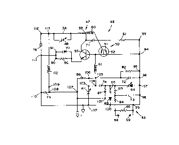
The r f transmitter circuit of transmitters 14, 15 and 16 is shown in
detail in Figure 2. The preferred embodiment of the transmitter includes
surface acoustic wave (SAW) device 50, transistor 55, coils 60, 61 and 62,
voltage variable capacitor 64, variable capacitors 67 and 68, capacitors 70
through 76, resistors 80 through 88, and diode 89. The SAW device 50 is
preferably a surface acoustic wave resonator (SAWR) 51 packaged in a protective
~Z'7~ 9
--6--
case 52. One side of the SAWR 51 is connected to coil 60 and the other is
connected to the base o~ transistor 55. The case 52 of the S~W device 50 is
connected to ground. The emitter of transistor 55 is connected to ground
through resistor 80 and capacitor 70 which are connected in parallel. The
collector of transistor 55 is connected to ground through capacitor 71 and
resistor 81 in series, to the other side of coil 60, and to ground through the
antenna 34 (which is a trace on the microchip and shall be discussed further
below) and capacitor 76. Variable capacitor 68 is connected in parallel with
antenna 34. Coil 62 is connected between antenna 34 and the positive power
supply voltage (V+). Capacitor 75 is connected between the positive voltage
line and ground. The line between the SAWR 51 and the base of transistor 55 is
connected to a modulation circuit 49 generally located in the lower right
corner of Fig. 2. (Insofar as the rest of the circuitry interacts with the
modulation circuitry 49, it also may be considered part of the modulation
circuit 49.) Or,e side of coil 61 is connected to the line between SAWR 51 and
the base of transistor 55. The other side of the coil Çl is connected to
ground through resistor 82 and capacitor 72;in parallel and through variable
capacitor 67; the same side of coil 61 is also connected to the positive
voltage line through resistor 88 and to one side of capacitor 74. The other
side of capacitor 74 is connected to the positive voltage line through resistor
87, to ground through resistor 86 and diode 89 ~onnected in series with the
cathode of the diode toward ground, to ground through voltage variable
capacitor 64, and to the data input line 58 through resistors 83 and 84. The
line between resistors 83 and 84 is connected to ground through capacitor 73.
The line 59 represents the ground side of the data input circuit. Resistor 85
is connected between data input lines 58 and 59 which connect to the signal
processing circuitry ~33, 36 or 39).
Turning now to Figure 3, the microcircuit traces are shown. That is, in
the preferred embodiment, the circuit of Fig. 2 is placed on an integrated
circuit chip or printed circuit board and the various connections are made via
9~
--7--
metallic traces printed on the chip. There are two major traces: the ground
trace 115 indicated by a broken line and the positive voltage trace 116
indicated by the solid line. Traces 115 and 116 are separated on the IC chip
or printed circuit board by an insulating layer. An approximately 1/8" x 1"
portion 34 of trace 115 acts as the r-f antenna when a printed circ~it board is
used. ~hen this circuit is used in a shielded hybridized (miniaturized)
circuit, a separate antenna must be used to radiate the eneryy outside the
shield. A third trace 117 usPd for connecting four circuit elements is also
shown. Other conventional traces as generally indicated by the remaining
cirGuit lines of Figure 2 are also on the chips or printed circuit boards but
are not shown. The connections to the three traces shown are indicated by
black dots, such as 107, and correspond to the circuit points having the same
numbers on the circuit diagram of Fig. 2. The structure of the traces shown is
important if the proper oscillation of the circuits is to be obtained, although
similar traces may be used and tun~d to the proper oscillation frequencies as
is known in the art.
In the preferred embodiment, SAW devic,e 50 is a UHF 315 megahert~ zero
degree phase surface acoustic wave resonator, transistor 55 is a bi-polar type
2SC2876, and coil 60 is a 6 turn .125 inch diameter, thirteen-thirty-second
inch long, air core coil made of #28 A.W.G. wire. Preferably, coil 61 is a .47
microHenry fixed coil and coil 62 is a 1.5 microHenry fixed coil. Voltage
variable resistor 64 is preferably a type MV2105 AFC si1icon Epicap diode
(available from Motorola, Inc.), and variable capacitors 67 and 60 are 5-35
picofarad capacitors.
Capacitors 70, 73, 75 and 76 are preferably 470 picofarad while 71 is a
1000 pf, 72 is a 94 pf, and 74 is a 47 pf capacitor.
Resistors 83~ 84 and 86 are preferably lOOK ohm resistors, resistor 80 is
a 100 ohm resistor, 81 is a 47K ohm resistor, 85 is a 600 ohm resistor and 87
is a 2 megaohm resistor. Diode 89 is a type lN4148. The traces s~ch as 34,
are preferably of copper.
--8--
The other components of the invention as shown in Figure I may be
conventional; for example, components as described in the patents enumerated
above. Preferably, however, the signal processors are programmed to produce a
Manchester digital signal having a voltage level of from about zero to 5 volts
at about 4 kilohertz.
The circuit functions as follows. SAWR 51, transistor 55, capacitor 76
and coil 60 form a Pierce oscillator circuit with the SAWR 51 dominating the
oscillation frequency. The transistor 55 is the active amplification element.
The SAWR 51 and coil 60 may be considered to be the principal elements of a
feedback circuit 48. The fundamental or "centerline" frequency is preferably
tuned by mechanically adjusting the separation of the turns of coil 60. The
line including capacitor 71 and resistor 81 shunts the SAWR 51 indirectly, with
capacitor 71 blocking DC current and resistor 81 serving as a load and a
circuit Q regulator (see discussion of Q below). The shunt shortens the
startup time of the oscillator circuit 47. Capacitor 75 is a bypass capacitor
to prevent r-f energy from entering the modulator portion of the circuitry
through ground. Coil 62 has a lower resonant frequency than the rest of the
circuit and serves as a choke to prevent the antenna energy from feeding
through capacitors 75 and 76 into the biasing circuitry (see below) of the
transistor 55. Variable capacitor 68 may be used to tune the antenna resonant
frequency. Capacitors 71, 75 and 76 are chosen to be low in capacitive
resistance so as not to cause significant thermal stability problems.
The modified Pierce oscillator circuit 47 further includes coil 61 and
variable capacitor 67 which, as will be further discussed below, also can be
considered part of the modulation circuitry. These two elements tune both the
centerline frequency of oscillation and the modulated frequency. Resistors 88
and 82 and coil 61 set the D.C. bias point for transistor 55 to determine the
gain for the transistor. Resistor 80 and capacitor 70 further re~ine the` gain
adjustment, preventing degeneration of the gain in low battery situations.
- 9 -
The modulation circuit is primarily composed of capacitors 72, 73, 74,
resistors 83 through 87, variable capacitor 67 and voltage variable capacitor
(VVC) 64, of which the latter is the most important element. Capacitor 72
shunts the V~C and trimmer capacitor 67. Capacitor 72 is selected to be
temperature compensating for VVC 64. Capacitor 73 and resistor 8~ form a
filter networkO Resistor 85 provides a consistent low impedance load for the
incoming data signal and is sized to match the circuit used in signal
processors 33, 36 or 39. The resistors 83 through 87 together form a D.C.
voltage divider that helps prevent undesirable negative voltages from occurring
at the cathode of VVC 64. Capacitor 74, resistor 86 and diode 89 provide a
shunt line for both the trimming circuit (61 and 67) and the modulatiun
circuit, with capacitor 74 preventing D.C. current flow, resistor 86 serving as
a load to prevent excessive power flow from the circuits shunted, and diode 89
acting as a voltage regulator for the resistance divider network.
The centerline frequency and the deviation frequency (the amount the
frequency deviates when modulated) are preferably adjusted by trimming variable
capacitor 67. The frequency may also be adjusted by trim~ing coil 61. The
latter trimming is performed by mechanically moving the coil turns slightly in
relation to one another. (In a hybrid version of the transmitter which I have
built, the mechanical trimming of the coil 61 is the preferred method of
adjusting the frequencies.) Coils 60 and 61 may be changed to allow for
different centerline and deviation frequencies than those discussed herein.
These coils play an important role in maintaining the feedback energy in a
positive rather than negative phase, thus sustaining the oscillations. These
coils are unique in that their Q is quite low compared to the conventional Q
values that would be provided in a circuit of this type. The low Q of these
coils is an important factor in obtaining the low total Q of the feedback
circuit (see below).
The operation of the circuit is as follows. The oscillation of the basic
r-f oscillator circuit 47 is stabilized by the feedback portion 48 of the
~g~3~39
-10-
circuit which includes SAW device 50. (The oscillation frequency may be tuned
by trimming coi1 61 in some embodiments.) The oscillation of the feedback
circuit, and thus the oscillation of the whole circuit, is modulated by the
data input in the following manner. Voltage variable capacitor 64 responds to
a change in the data input voltage to change the capacitance of the modulation
circuit. The changed capacitance of the modulation circuit causes its
oscillation frequency to shift. The modulation circuit parallels the S~WR
circuit and a change of its resonance frequency therefor causes the effective
resonance of the entire circuit to change. The modulated circuit may be
thought of as "pulling" the normal SAW resonance frequency to the modulated
frequency. In the circuit shown, a data input voltage change of about 5 volts
causes a change in oscillation frequency of about 60 to 90 kilohertz, depending
on the tuning. Changes of 100 kilohertz and above have been obtained.
Preferably, both the overall SAWR centerline frequency and the modulation
frequency (frequency deviation) are tuned simultaneously using the variable
capacitor 67 (or coil 61).
The security system of the present inv;ention utilizes frequency shift
keying (FSK), thouyh other frequency modulation may be used. The signal
processor, such as 33, 36 or 39, produces digital signals comprising a series
of voltage transitions between a high voltage value (preferably 4 to 5 volts)
and a low voltage value (preferably 0.1 to 0.4 volts). The signals are
preferably Manchester encoded, which permits the synchronization with the
recejver in the central station 18 to be updated regularly. Other digital
encoding systems may be used, however,
Figure 4 shows three examples of Manchester encoded signals. Each of the
three samples contains a preamble portion (at the left in each sample) that is
a series of Manchester encoded l's. This preamble allows the transmitter time
to warm up and the receiver time to establish communication. (If a few data
bits at the front end are lost, it creates no problem.) Each sample also
includes a central portion of zero voltage (not Manchester encoded) which
~7~
-11-
provides a transition to the significant data bits which follow. Note that
even where the signal is all O's or all l's (as in the right hand portion of
samples Nos. 2 and 3 respectively) the Manchester system makes regular
transitions between the low and high voltage values. This is the feature that
permits the regular synchronization with the receiver.
The voltage transitions of the digital signal (Manchester or otherwise)
will, as described above, cause a corresponding freqwency shift of the
transmitted r-f signal of the order of 60-9C kilohertz. The frequency shift is
keyed on by the receiver in station 18 to recreate the digital voltage signal.
The security system according to the invention is much more reliable than
prior art security systems due to the superior frequency stabilization and low
power consumption of the transmitter. The SAW stabilized transmitter does not
have the temperature shifts and drift problems associated with conventional LC
and RC type oscillator/transmitter devices3 and does not have the power supply
and battery failure nv"blems associated with the prior art bulk crystal
oscillator circuits. The SAW oscillator/transmitter does not exhibit the
spurious modes of oscillation that marred p~ior art transmitters. In addition,
the power levels of the harmonic oscillation frequencies are greatly attenuated
from the fundamental frequency as compared to prior art
oscillators/transmitters.
A feature of the invention is the on-board antenna and output antenna load
simulation which result in high oscillator startup reliability, which is useful
in a transmitter that must start up many times from.a de-energized condition.
Further, the operating voltage range of the transmitter is very broad, ranging
from 3V DC to 12V DC with only a slight frequency change.
The invention is the first workable FM SAW oscillator/transmitter. An
important factor in producing the workable FM SAW oscillator/transmitter is the
reduction of the Quality ratios ~Q) of the feedback circuit in comparison to
conventional circuits. Q may be defined either in terms of bandwidths, which Q
we shall refer to herein as Qbw ~ or in terms of impedance (Z) and resistance
~LZ~ 9
-12-
(~) which we shall refer to herein as QZR . It is noted that Q is a relative
term and that the two Q values are not equal in general. Qbw may be defined
as Qbw = Fo/~ F where Fo is the fundamental frequency (3l8 megahertz in the
preferred embodiment) which is given by the equation Fo= l/27r ~ where L is
the inductance and C is the capacitance, and a F is the frequency change in
modulation (60-lO0 kilohertz generally in the preferred embodiment). QZR may
be defined as QZR = Z with Z given by Z = (Xl - Xc), where Xl is the inductive
reactance and Xc is the capacitive reactance, and R is the DC and skin effect
resistance. Conventional transmitter design strives to maintain high Q
feedback circuits. It was believed the Qbw should be about 16 ~( 103 in
feedback circuits in order to obtain suitably high output power to have an
acceptable transmitter broadcast range. (The broadcast range should be at
least 200 feet for security transmitters.) However, SAWR based oscillation
circuits of high Qbw tend to flip into free running modes. It is a feature of
the invention that the Qbw of the feedback circuit is unusually low, typically
below 12 x 103. Preferably, Qbw iS about 3 x 10³. It is also a feature of
the invention that the coils 60, 6l are made of a wire that is much smaller in
diameter than typically used in oscillation circuits of this type. Reduction
of the wire diameter is important in establishing the low QZR required for
frequency pullability suitable for FSK. The reduction of the wire diameter
increases the resistance by limiting current an~ reducing the electrical cross
section thus increasing the r-f skin effect. In the SAWR circuit, the
reactances, Xc and Xl, generally must remain const~nt for a constant frequency
so that resistance becomes the significant variable. With the proper biasing
of transistor 55, as discussed above, broadcast ranges of up to 900 feet have
been obtained~ despite the low Q values. This broadcast range is greater than
that of the majority of prior art security systems. The FM SAW transmitter of
the present invention is particularly useful in a security system because it is
not susceptible to the noise and interference problems that disrupt AM SAW
transrnissions beyond usefulness.
~L _13
Another feature of the invention is that it is manufactured on a single IC
chip. Prior to the present invention, it was not thought possible to place
such a transmitter on a chip. The design of the traces given above is
important for this.
Still another feature of the invention is the unusually fast startup time
of the SAWR transmitter. Such fast startup results in less loss of data and
shorter transmission times.
An important feature of the invention is the relatively large shifts of
frequency obtained. As indicated above, frequency shifts of 60 - 90 kilohertz
are routine and shifts of 100 kilohertz have been obtained. Prior to the
present invention, it was thought that such high frequency shifts would cause
the SAW device to go into a free running mode and not return to the fundamental
frequency.
Still another feature of the invention is the use of a variable voltage
capacitor or tuning diode to modulate the SAWR circuit. It is possible with
the design shown to modulate down to zero volts. This was never done on an FM
transmitter IC chip prior to the present inyention.
Although, for clarity, the r-f transmitter circuit of Figure 2 has been
discussed in terms of an oscillator circuit 47, a feedback circuit 48, and a
modulation circuit 49, it should be understood that an r-f circuit oscillates
as a whole and thus from other points of view the modulation circuit may be
considered to be a part of the feedback circuit and/or the oscillation circuit.
A novel security system having a frequency modulated transmitter employing
a SAW device and having numerous other features has been described. It is
evident that those skilled in the art may now make many uses and modifications
of the specific embodiment described without departing from the inventive
concepts. Many other equivalent electronic elements and materials may be used.
For example, different amplifiers may be substituted for transistor 55, other
inductance combinations may be employed, different trace designs and materials
may be substituted, the circuit may be made other than on a chip, and so on.
14-
Many variations of remote sending units and receiving stations may be used.
Many types of frequency modulation may be used and many kinds of encoding
systems, digital or otherwise, may be used. Other SAW devices may be used: for
example I have successfully used an 180 degree phase SAW oscillator in a
similar FM transmitter circuit. Consequently, the invention is to he construed
as embracing each and every novel combination of features present in the
security system described.