Note: Descriptions are shown in the official language in which they were submitted.
3;~
~ACRGROU~ OF THE INVE~TIO~
The present invention relates to a method and to a
meacuring instrumen~ for identifying the diffusion length of
minority charge carriers and of their topical fluctuations for
non-destructive detection of flaws and impurities in a
semiconductor crystal body.
For qualitative characterization of the material of a
semiconductor crystal, it is known to identify the diffusion
length of the minority charge carriers therein since this is
valid measurement of the number of recombination centers and
traps in the semiconductor crystal. Two methods are standard for
identifying the diffusion length of the minority charge carriers
in a semiconductor crystal, measuring photoconductivity
(photoconductive decay) and measuring the surface photovoltage.
Both methods are disclosed in the text "Library of Congress
Cataloging" in "Publication Data of ~exas Instruments Elec.
Ser.", edited by Tyler G. Hicks and Lester Strong, 1975, pages
105 through 129.
In measuring the photoconductivity, the semiconductor
is irradiated with light such that electron hole pairs are
generated and the change in conductivity is subse~uently
measured. The life time and, thus, the diffusion length of the
minority charge carriers are capable of being identified
therefrom. The shape of the semiconductor crystal is thereby of
significance for the measurement and the semiconductor crystal
must usually be destroyed before the measurement.
A surface photovoltage occurs when a semiconductor
crystal is irradiated and can be measured by capacitative
coupling~ The surface photovoltage can be used to measure the
diffusion length of the minoxity charge carriers. This method,
l~.d ~
however, has the disadvantage of a long measuring time since
measurements with different light wavelengths must be
successively carried out. Further, the topical resolution of the
measurement is low since the irradiated area must have a size of
at least 1 cm .
S~MMARY OF THE INVENTION
An object of the present invention is the measuring of
the diffusion length of minority charge carriers in a
semiconductor crystal body with optimum precision.
The invention is characterized by a method of the type
initially cited wherein:
a) the semiconductor crystal body is positioned between
two electrolyte-filled measuring chamber halves such
that a front slde and a backside of the semiconductor
crystal body are each in contact with the electrolyte
of the measuring chamber;
b) the semiconductor crystal body is connected to a
voltage source via an ohmic contact and a voltage is
applied between the backside of the semiconductor
crystal body and an electrode of the measuring chamber
half connected to ~he backside of the semiconductor
crystal body, so that a bloc~ing space charge zone
arises at the backside of the semiconductor crystal
body;
c) the front side of the semiconductor crystal body is
irradiated with light;
d) the photocurrent IG of the minority charge carriers 6 S
occurring at thé ~ackside of the semiconductor crystal
body upon irradiation is measured; ~ h~
.
--3--
e) a voltage is applied between the front side of the
semiconductor crystal body and an electrode of the
measuring chamber half connected to the front side of
the semiconductor crystal body, so that a blocking
space charge zone is formed at the front side of the
semiconductor crystal body;
f) the photocurrent Io f the minority charge carriers
occurring at the front side of the semiconductor
crystal body upon irradiation is measured; and
g) the diffusion length L i5 calculated from the the
mathematical equation:
IG/Io = a 2 . L2 -2
2 2
1 -~ L exp(-D/L)+exp(+D/L)
~1here a is the absorption coefficient and D is the
specimen thickness.
The method is implemented with a measuring instrument
that is characterized by:
a) two measuring chamber halves held by a frame that can
be i.ndividually filled with electrolyte and each of
which contains an electrode;
b) a holding mechanism for the semiconductor crystal body
which is designed such that the semiconductor crystal
body can be positioned between the measuring chamber
halves, so that the front side and the backside of the
semiconductor crystal body are each in contact with
the content of a measuring chamber half;
~) a terminal for producing an ohmic contact to the
semiconductor crystal body;
-4-
d) at least one light source such that a light ray is
directed on~o the surface of the semiconductor crystal
body;
e) a dc voltage source for applying a dc voltage between
the semiconductor crystal body and the electrolyte;
and
f) an ammeter means.
BRIEF DESCRIPTION OF T~E DRAWINGS
The features of the present invention which are
believed to be novel, are set forth with particularity in the
appended claims. The invention, together with further objects
and advantages, may best be understood by reference to the
following description taken in conjunction with the accompanying
drawings, in the several Figures in which like reference numerals
identify like elements, and in which:
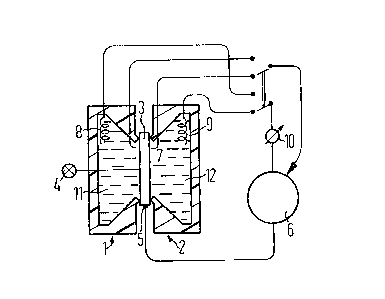
FIG. 1 is a schematic illustration of a measuring
instrument for implementing the method of the present invention;
FIG. 2 schematically depicts a crystalline
semiconductor wafer having impurities;
FIG~ 3 shows the topical distribution of the
impurities of the semiconductor wafer of FIG. 2.
FIG. 4 is a perspective view of a measuring chamber
half having a holding:device for a semiconductor crystal body.
DESCRIPTION OF THE PREFERRED F~BODIMENT
As shown in FIG.:l, a semiconductor crystal body 3 is
situated between two electrolyte-filled measuring chamber halves
1 and 2. a connection betweèn the semiconductor crystal body 3
and a controlled constant voltage source 6 (for example, a
~ ~ -5-
7~
potentiostat) is produced via an ohmic contact 5. A constant
voltage is produced between the ohmic contact 5 and the electrode
9 that is situated in the electrolyte 12 of the second measuring
chamber half 2. The backside of the semiconductor crystal body 3
thus is in contac~ with the electrolyte 12 of the second
measuring chamber half 2. A surface-proximate electrode 7 for
measuring the voltage at the surface o~ the semiconductor crystal
body 3 is located at the backside of the semiconductor crystal
body 3, so that the constant voltage can be controlled with the
measured voltage. The front side of the semiconductor crystal
body 3 that is in contact with the electrolyte 11 of the first
measuring chamber half 1 is irradiated with laser light from a
laser 4. The light ray is deflectable by an apparatus (not
shown) such that individual points on the surface of the
semiconductor crystal body 3 can be designationally irradiated.
For example, the deflection device for the light ray can be
composed of an arrangement of mirrors.
During the measurement, the front side of the
semiconductor crystal body 3 is scanned with the laser beam 4.
The scan speed is typically 1 through 100 cm/sec for a spot size
of 1 mm2. The backside of the semiconductor crystal body 3 is
located in the dark during the measurement and is positively
biased relative to the electrolyte 12 before the measurement for
an n-silicon semiconductor and is negatively biased relative to
the electrolyte 12 for a p-silicon semiconductor. Constant
voltages between 2 and 5 volts are typically selected. The
silicon electrolyte contact then behaves like a diode polarized
in a non-conducting direction, i.e., only a small leakage current
flows. No voltage is applied between the front side of the
semiconductor crystal body 3 and the electrolyte 11 of the first
--6--
measuring chamber half 1. The electrolyte 11 serves the purpose
of providing saturating surface conditions. The electrolyte 11,
12 is the same in both measuring ~hamber halves and, for example,
can be composed of two percent hydrofluoric acid that has a fe~
drops of a wetting agent added. Before the measurement it may be
necessary to strip undesired surface layers on the ~emiconductor
crystal body by electro-polishing.
The minority charge carriers generated by irradiation
of the front side of the semiconductor crystal body 3 diffuse
through the semiconductor crystal body and recombine at potential
recombination centers. The charge carriers that proceed up to
the backside of the semiconductor crystal body 3 are acquired by
the electrical field present there and are measured as
photocurrent ~G by the ammeter 10. It is advantaqeous to use a
loc]~-in amplifier in the detection of the photocurrent IG. The
level of the photocurrent IG detected at the backside of the
semiconductor crystal body 3 in relationship to the photocurrent
Io generated at the front side of the semiconductor crystal body
3 is a measure of the density of the recombination centers of the
semiconductor crystal body 3 and is thus linked to the minority
charge carrier diffusion length L derived from the mathematical
equation:
IG/Io = ~ 2 L2 . 2
1 2L2 exp(-D/L)+expt+D/L)
where~D is the thickness of the semiconductor crystal body
and is the absorption coefficient. The portrayal of the
photocurrent IG as a function of the coordinates of the laser
beam incident on the front side produces an image of the
distribution of the recombination centers in the volume of the
semiconductor crystal body 3.
The photocurrent Io is measured while a constant
voltage is applied between the front side of the ~emiconductor
crystal body 3 and the electrolyte 11 of the first measuring
chamber half l while the front side of the semiconductor crystal
body is being irradia~ed. No voltage is applied to the back side
of the semiconductor crystal body 3 during the measurement of I
FIG. 2 depicts two lines of an iron impurity 22
situated on a crystalline semiconductor wafer 21. The line 23
marks the edge of the measuring area that is established by the
geometrical dimensions of the measuring chamber halves l and 2.
FIG. 3 depicts a topically resolved measurement of the
photocurrent IG ~hich exhibits minimums 31 at those locations
where the lines of iron impurity 22 are situated on the
crystalline semiconductor wafer 21.
FIG. 4 depicts an embodiment of a measuring instrument
having a central frame 41, having a holding mechanism having a
holding frame 42 and an adaptor 43 for different semiconductor
crystal bodies and having two measuring chamber halves of which
only one (41) is shown in FIG. 4. The adaptor 43 can accept
semiconductor crystal bodies having diameters from lOmm through
200mm and having thicknesses of a few lO0 ~m up to several
millimeters. The carrier plate 44 of the measuring chamber half
l is pressed against the central frame 41 by a pneumatic means
(not shown in FIG. 4) such that sealing lips 45 of the measuring
chamber half l adhere firmly to the semiconductor crystal body.
The sealing lips 45 of the measuring chamber half l compensate
for small irregularities of the semiconductor crystal body so
that the crystal body need not be either round or entirely
planar. Like the adaptor 43, the carrier plate 44 can be adapted
to the respective semiconductor crystal body size.
--8--
~ he outer cover plate 46 of the measuring chamber half
1 is optically transparent and can be mounted on the carrier
plate 4~. The entire part of the measuring instrument containing
electrolyte is resistant to acid, particularly hydrofluoric acid,
and is preferably manufactured of polyvinyl chloride or Teflon.
The transparent cover plate 46 can be fabricat~d of acrylic or
silica glass that is either periodically changed or is coated
with a thin protective layer. When the measuring chamber half 1
is pressed onto the semiconductor crystal body, an ohmic contact
is produced by ring a 47 of measuring tips The ring 47 of
measuring tips can be provided with a plurality of measuring
instruments, so that a check can be carried out therewith to
determine if the electrical contact to the semiconductor crystal
body is ohmic. The ring 47 of measuring tlps can be optionally
used instead of the ohmic contact shown in FIG. 5. Leads 48
provide for delivery of electrolyte, vacuum and compressed air.
The invention is not limited to the particular details
of the apparatus depicted and other modifications and
applications are contemplated. Certain other changes may be made
in the above described apparatus without departing from the true
spirit and scope of the invention herein involved. It is
intended, therefore, that the subject matter in the above
depiction shall be interpreted as illustrative and not in a
limiting sense.