Note: Descriptions are shown in the official language in which they were submitted.
34-5/Tri-Pack/90236/a/Dec.8 ~ 3~500
FIELD Of IN~ENTION
This invention relates to a universal low level voltage programmable
logic control for protecting electrical power systems against damage
caused by overloads and faults, and particularly relates to a
programmab1e, logic control that activates a circuit breaker or trip
device.
BACKGROUND TO THE INVENTION
Circuit breakers are commonly used for protecting electrical circuits
10 and devices from damage due to circuit overloads and ground faults.
Circuit breakers embodying thermal and magnetic mechanisms have
heretofore been used to trip the circuit breaker upon over current
conditions. Some of these earlier devices included interchangeable
trip units so as to provide trip current ratings that could be
changed without changing the entire circuit breaker.
Furthermore, shunt trip mechanisms have been developed to co-ordinate
and provide interaction between circuit breakers on complex
electrical distribution circuits so that circuit breakers on
different parts of the electrical system would trip at different
20 levels and different time delays upon the occurrence of electrical
faults.
i;~ 8 0 S 0 0
For example, Un;ted States Patent No. 3,826,951 disclosed a shunt
trip mechanism which utilized electronic circuits to analyze an
electrical signal produced by a sensing device such as a current
transformer to generate a trip command to a shunt trip mechanism upon
occurrence of an electrical fault.
Circuit parameters which have heretofore been monitored in order to
activate such trip devices include:
(a) the level of fault current
(b) ground fault detection
(c) the maximum level of continuous current the circuit
interrupter can withstand without damage
In order to minimize the cost in providing different circuit
interrupters, various types of circuit interrupters having mechanical
interchangeable circuit configurations have been developed.
For example, United States Patent No. 4,210,887 discloses a circuit
interrupter having interchangeable trip circuits removably disposed
in a circuit interrupter housing and connected between a current
transformer and a trip mechanism and includes rejection structure to
ensure that only trip unit housing circuitry compatible with the
20 electrical characteristics of the circuit interrupter can be inserted
into the housing.
. .......................... .
'..~' ~ ' ~ '
` ` '
- ~ -
1)0
Some devices utilize several current transformers in order to monitor
a range o-f electrical characteristics whereby edch current transfer
used in association with the electrical device provide a portion of
the range of electrical characteristics monitored. Other devices
utilize several devices in association with current -transformers in
order to monitor a range of electrical characteristics of an
electrical system whereby each device provides a portion of the range
of electrical characteristics monitored.
Such structures however present relatively complicated devices.
10 It is an object of this invention to provide a programmable logic
control which is simple to construct and use.
It is a further object of this invention to provide a programmable
logic control which has greater accuracy and selectivity than other
circuit interrupting devices.
FEATURES OF THE INVENTION
The broadest aspect of this invention relates to a
universal programmable logic control device for monitoring the
current of a circuit and for signalling a control device said
programmable logic control device including; electrical power
20 circuitry for activating said control devicei electrical circuitry
for monitoring said current in the electrical circuit said
1280500
electrical circuitry including, adjustable electrical signal input
circuitry to match the programmable logic control device to the
electrical current in said circuit, adjustable pick-up circuitry for
adjusting the level of current monitored in the electrical circuit,
and adjustable time circuitry for adjusting the time duration of the
selected level of electrical current, so as to commard the electrical
power circuitry to activate the control device when the electrical
current in the electrical circuit reaches the selected level and time
duration and means for controlling the level of voltage applied to
10 the adjustable pick-up circuitry and time circuitry substantially
without resistive burden, said means passing a reference voltage
which is less then an input voltage to said means.
Another aspect of this invention relates to a universal
programmable logic control device for monitoring the electrical
current in a circuit and for signalling a trip device for activating
a circuit breaker in the electrical circuit, including; electrical
power circuitry for activating the circuit breaker; electrical
circuitry for monitoring the value of current in the electrical
circuit, said electrical circuitry including, adjustable ampere taps
20 to match such universal programmable logic control device to the
electrical current, in said circuit, adjustable pick-up circuitry for
adjusting the level of current monitored in the electrical circuit,
. adjustable time circuitry for adjusting the time duration of the
: selected level of current, so as to command said electrical power
circuitry to activate said circuit breaker when said current in said
`. electrical circuit reaches said selected said level and time duration
Y~
,;~,
:
,:~ ~ . -- - '
. . ' ' ' ', ' .
; ~ - -
, : ' - - ' `,
~ 5 ~ 1 Z 8 0 5 0~]
and means for controlling the level of voltage applied to the
adjustable pic~-up circuitry and time circuitry substantially without
resistive burden, said means passing a reference voltage which is
less than an input voltage to said means.
Yet another aspect of this invention relates to a
universal programmable logic control device for monitoring the
current of a circuit and for signalling a control device, said
programmable logic control device including: electrical power
circuitry for activating said control devicei electrical circuitry
10 for monitoring said current in the electrical circuit, said
electrical circuitry including adjustable pick-up circuitry for
adjusting the level of current monitored in the electrical circuit,
and adjustable time circuitry for adjusting the duration of the
selected level of electrical current so as to command the electrical
power circuitry to activate the control device when the electrical
current in the electrical circuit reaches the selected level and time
duration; and means for controlling the level of voltage applied to
the adjustable pick-up circuitry and time circuitry substantially
without resistive burden, said means passing a reference voltage
20 which is less than an input voltage to said means.
DESCRIPTION OF THE DRAWINGS
Figure 1 is a schematic view of the programmable logic
control device.
' `
.,~ . ,
:
1'~8()SOO
Figure 2 is a detailed electric~l circuit drawing of the
comparator circuitry.
Figure 3 ;s a detailed electr;cal circuitry of the long
time delay short time delay, ground pick-up and ground delay
circuitry of the programmable logic control device.
Figure 4 is a detailed drawing of the long time pick-up,
short time pick-up, and instantaneous pick-up circuitry of the
programmable logic trip device.
Figure 5 is a detailed electrical circuit drawing for the
10 light emitting diode.
Figure 6 is a detailed electrical circuit drawing of the
long time pick-up circuitry of the programmable logic control device.
Figure 7 is a detailed electrical circuit drawing of the
reference voltage ground and long time pick-up.
Figure 8 illustrates comparator circuits for
instantaneous and short time for reference voltage.
-
.
128()SOO
Figure 9 illustrates the target circuitry.
Figure 10 illustrates circuitry for signal to actuator.
Figure 11 illustrates circuitry for reference voltage forall functions.
Figure 12 is a table showing the ampere taps ranges
available for various current transformer ratings for the
programmable logic trip device.
Figure 13 is a top plan view of the control panel of the
programmable logic trip device.
Figure 14 is a graph showing the Long Time, Short Time
and Instantaneous Time current characteristics of the programmable
logic control device.
Figure 15 is a graph showing the Ground Time
Characteristics of the programmable logic control device.
DETAILED DESCRIPTION OF THE INVENTION
Identical parts have been given identical numbers
throughout the figures.
.,~
`~
.
.
.~ :
.
`' . '
~80500
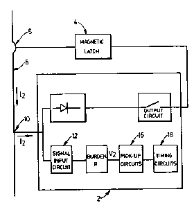
Figure 1 discloses generally the programmable logic
control device 2 which controls or commands a control device such as
the trip device 4 which is a magnetic latch which trips the circuit
breaker 5 in the case of abnormal conditions in the electrical
conduc-tor 6 of an electrical power system (not shown). It should be
noted however that the programmable logic control device 2 could also
be utilized to signal other control devices to activate light
switches or other switches to activate electrical motors or the like.
The programmable logic control device 2 is connected to
10 an electrical sensing device mounted on the conductor 6, namely, a
sensor 10. Such sensors 10 typically consists of a current
transformer which is well-known to those persons skilled in the art.
Such sensor 10 is connected to the programmable logic control device
2 by suitable electrical wiring.
The programmable logic control device 2 includes a signal
input circuit 12, a burden resister R, pick-up circuits 16 and timing
circuits 18 generally depicted in Figure 1 and more fully
particularized in figures 2 to 11 inclusive.
The sensor 10 supplies the programmable logic control
20 device 2 with a signal I2 which is proportional to the primary
current Il in the electrical conductor 6. The sensor 10 also
provides the bias-power required to operate the circuit trip device 4
and the circuitry of the programmable logic control device 2. The
sensor 10 is switched to the trip device 4 to open the circuit
; `
' ` `
.
iL'~8() S O ~
breaker 5 when the primary current Il exceeds the selected mdgnitude
and time-delays as more fully particularized herein. The trip device
or magnetic latch 4 is powered by the line over current through the
sensor 10 and the programmable logic control device.
Furtheremore it has been found that by separating the
power box from the control board harmonics are substantially reduced
or filtered out.
The secondary current I2 is rectified in the programmable
logic control device 2 and is burdened with a resistor R which is
10 selected by selection of suitable ampere-tap plugs. The ampere-taps
available for the programmable logic control device 2 do not depend
on the frame size of the circuit breaker and are listed in Figure 5.
As can be seen from Figure 5 the ampere tap plugs utilized in the
programmable logic control device 2 for the transformer current
ratings illustrated in Figure 5 can be utilized to modify the current
rating by a ratio of .5, .75 or 1Ø In other words if we are
monitoring a 3000 amp conductor 6 we would utilize a 4000 amp current
transformer and select the appropriate ampere tap plug of RBl, RB2,
RB3, illustrated in Figure 2 at .75 in order to monitor a primary
20 current of 3000 amps through conductor 6.
Similarily a 300 amp primary current Il could be
monitored by utlizing a 600 amp current transfomer and an ampere tap
multiple of 0.5.
- ~.
: "
lo -
~28050l)
By utilizing different ampere-taps, as described herein,
the programmable logic control device 2 is capable of monitoring and
controlling circuits having a wide range of current characteristics
which may be easily and quickly changed so as to accommodate a great
variety of current ranges.
Once the appropriate ampere-taps have been selected as
described herein, a voltage V2 is developed across the burden
resistor R which voltage is proportional to both the primary current
Il and secondary current I2.
The electrical pick up circuits are activated by ~2 if it
exceeds a particular selected level.
The electronic pick-up circuits 16 consist of Long Time
Pick-up, Short Time Pick-up, Instantaneous Pick-up, and Ground
Pick-up, as are more fully described herein.
If any of the electronic pick-up circuits 16 are
activated then the time delay circuits 18 are activated to determine
that V2 and therefore Il have persisted for a pre-determined and
selected time interval.
~; At the expiration of the delayed time, the output circuit
20 is triggered so as to enable the power supply from sensor 10 to
,~ activate the magnetic latch 4 and thereby opening the circuit breaker
~` 5.
.
~ ' '.
. ~ - . ~ ' ' , ,
. .
: - . . ' . -~ ,
`
: ~ :
30S~O
As best illustrated in Figure 2, Zener diodes Z01, Z02,
Z04 and Z06 are used in reverse mode so as to drop the voltage
substantially without resistive burden. Figure 2 shows the Zener
diode Z01 has a rating of 33 volts. If Zener diode Z01 was used in
the normal mode once the current applied to the anode side reached 33
volts, Zener diode Z01 would open or gate to let all of the voltage
through. In the invention disclosed herein Zener diode Z01 is
utilized in the reverse mode so that when the input voltage applied
to the cathode side of the Zener diode Z01 reached the rating of 33
10 volts, Zener diode Z01 will allow only the excess through. For
example, if an input voltage of 100 volts is applied to the cathode
side of Zener diode Z01, a reference voltage of 67 volts passes
through. Therefore the use of Zener diode Z01 in the reverse mode
substantially eliminates wave distortions on the line.
Zener diode Z01 is used for giving a voltage drop of 33
volts for the phase voltage without substantially adding any
resistive burden.
Zener diode Z02 is used for giving voltage drop of 20
volts without substantially adding any resistive burden for powering
20 the static indicators.
Zener diode Z04 is used for giving a voltage drop of 30
volts without substantially adding any resistive burden and thus
providing an adjustment of the phase voltage.
, . - , '
..... - , - - - - :
- , -
" `` . : ' ', ' '
1 280500
Zener diode Z06 is used for providing a voltage drop of
33 volts for the ground voltage without substantially adding any
resistive burden.
Figure 13 shows in greater detail the control panel 30 of
the programmable logic control device 2.
The control panel 30 includes an adjustable Instantaneous
Pick-up Control Knob 32, adjustable Short Time Control Knob 34, an
adjustable Long Time Control Knob 36 and an adjustable Ground Pick-up
Control Knob 38.
10 Instantaneous Pick-Up
The Instantaneous Pick-up Control Knob 32 is utilized to
select the level at which the circuit breaker 5 will be substantially
instantaneously activated by the trip device 4. In other words, once
the current Il in conductor 6 reaches the level selected on the
Instantaneous Pick-up Control Knob 32, the output circuit is
triggered so as to enable the power supply from the sensor 10 to
activate the trip device 4 and open the circuit breaker 5. The
Instantaneous Pick-up Control Knob 32 is adjustable in several
stages. For example, the Instantaneous Pick-Up Control Knob 32
20 illustrated in Figure 13 is adjustable in 6 stages of 4, 5, 6, 8, 10
or 12 times the ampere-tap chosen. However such increment of stages
may have other values depending on the value of the resistors
selected in Figure 3.
l,
,~.
.
.,~ .
.. ~
.:
~ 13 ~ B()5()0
For e~ample, if the ampere-tap is selected for 800 amps
and one selects the setting 4 on Instantaneous Pick-up Control Knob
32, the circuit breaker 5 will be substantially instantaneously
activated once the current Il reaches a level of 3,200 amps.
Figure 14 more fully particularizes the time-current
characteristics of the instantaneous trip of the programmable logic
control device 2.
Furthermore, the programmable logic control device 2 also
includes an I2T On-Off switch 40 so as to enable the user to switch
10 into or out of the time current characteristics of I2T illustrated in
Figure 14.
Short Time Pick-Up
The Short Time Pick-up Control Knob 34 is utilized to
select the level at which the short time pick-up circuit will be
activated. For example, if the Short Time Pick-up Control Knob 34 is
selected at the setting 2, and the ampere-tap selected at 800 amps,
then the short time pick-up circuits will be activated when Il in
conductor 6 reaches 1,600 amps.
The Short Time Pick-up Control Knob 34 shown in Figure 13
20 is adjustable to 2, 3, 4, 6, 8 and 10 times the ampere-tap chosen.
However such increment of stages may have other values depending on
the value of the resistors selected in Figure 3.
' ~
:
,
.
'- 1~ `'
1$00
hlrthermore, programmable logic control device 2 also
includes a Short Time Delay knob 42 which may be adjusted so as to
select a minimum, intermediate or maximum setting which corresponds
to selected time settings of the time delay circuits 18.
Figure 14 more fully particularizes the time current
characteristics of the Short Time Pick-up of the programmable logic
control device 2.
In our example, if we select Short Time Delay knob 42 to
minimum and the Short Time Pick-up Knob at a setting of 2, then the
10 magnetic latch 4 will be tripped if Il reaches 1,600 amps for a time
period of approximately 0.1 seconds as shown in Figure 14. It should
be noted that the values illustrated in Figure 14 have a tolerance of
plus or minus lS percent.
Long Time Pick-Up
The Long Time Pick-up Control Knob 36 is utili~ed to
select the level at which the long time pick-up circuits will be
activated. For example, if the Long Time Pick-up Control ~nob 35 is
selected at 1.0 and the ampere-taps selected at 800 amps then the
long time pick-up circuit will be activated when Il in conductor 6
20 reaches 800 amps.
Furthermore, programmable logic control device 2 also
includes a Long Time Delay Control Knob 44 which may be adjusted so
;
15 -
~Z80~;00
as to select a minimum, intermediate or maximum setting which
corresponds to selected time settings of the time delay circuits 18.
Figure 14 more fully particularizes the time current
characteristics of the Long Time Pick-up of the programmable logic
I control device 2.
In our example, if we set Long Time Control Knob to
intermediate and the Long Time Pick-up Control l<nob 36 to 1.0 then
the magnetic latch 4 will be tripped if Il reaches 800 amps for a
time period of approximately 250 seconds.
The Long Time Pick-up Control Knob in Figure 13 is
adjustable in several stages. For example, the Long Time Pick-Up
control l<nob 36 illustrated in Figure 13 is adjustable in 6 stages of
0.6, 0.7, 0.8, 0.9, 1.0 and 1.1 times the ampere-tap chosen. However
such increment of stages may have other values depending on the value
of the resistors selected in Figure 4.
Ground Pick-Up
The Ground Pick-up function is optional and may be
included in the programmable logic control device 2 where it is
desirable to protect electrical systems against faults to ground.
20 Such ground faults including arcing faults which result in currents
having a magnitude which is less than the normal load current Il but
require detection due to the damage which may result from the arc.
.
.
, .
,
, . , . . . . ~ ~ .
, ~ . . , : , ~
' ~ . ~ ' '' , ' . -
: : . .. , .: . -
- : :
,' ' , ~ , . ~ ' . . . ~, . - :
:. . . ,: , .
- 16 ~ 1~8 0 5 0 O
It should be noted that the regulatory bodies in the
North American market place require that the maximum ground
protection be set at 1200 amps.
The Ground Pick-up current settings are independent of
the Instantaneous Time, Short Time or Long Time current
characteristics and measure the real value.
The adjustable Ground Pick-up Control Knob 38 may be
adjusted as shown in Figure 4 to 1, 3, 6, 8, 10 and 12 times 100
amperes so as to match the system.
10Furthermore, programmable logic control device 2 includes
a Ground Delay Control Knob 46 which may be adjusted so as to select
a minimum, intermediate or maximum time delay setting which
corresponds to selected time setting invervals of the time delay
circuits 18.
Figure 15 more fully particularlizes the time current
characteristics of the ground pick-up of the programmable logic trip
device 2.
For example, if we set adjustable Ground Pick-up Control
~ Knob 38 at 3 and Ground Time Delay Control Knob 46 at intermediate
,~ 20 then the magnetic latch 4 would be tripped if Il reaches 300 amps for
,~ a period of approximately 0.2 seconds.
^::
.. .. .
'~
~,.. : : . . .
. - - . - .
~ . -. - - :
'.'~: ' ~ ' ' ' ' ` ,
.
- 17 - ~ 8 O 5 0 O
Programmable Logic Control
The programmable logic control device 2 disclosed herein
allow the user to quickly select the desired control parameter of
instantaneous time, short time, long time and ground faults and to
change such parameters by adjusting the Control Knobs as well as the
ampere-taps. The programmable logic control device described herein
is therefore universal in the sense that one logic device can be used
to effectively monitor electrical systems over a range of electrical
characteristics by selecting the appropriate ampere tap and control
10 knobs which are incorporated in the device 2 rather than utilizing a
number of current transformers or logic devices. In the preferred
embodiment disclosed herein the programmable logic control device may
be universally utilized to monitor currents between a range of 30 to
4400 amps.
Moreover, if all of the control parameters are set then
the trip device 4 will be activated to open circuit breaker 5 when
primary current Il in conductor 6 reaches the value of the least
severe parameter selected for instantaneous time, short time, long
time or ground fault.
Furthermore the programmable logic control device 2 will
not trip the circuit breaker 5 when any of the adjusting Control
-~ Knobs 32, 34, 36 or 38 are moved from one setting to another since
the setting will be automatically raised to the highest value when
the Knob is between settings.
.~ .
,~;
' , . .- ,- ., ' ;''. ,, -:
. . . ' . - . . : ,'
- ~8~ 8(1500
Indicators
The programmable logic control device 2 also may be
equipped with optional indicators or targets, na~ely an
instantaneous/short time target 50, long time target 52 and ground
target 54. Target 50 will light up or indicate that the circuit
breaker 5 has been tripped when current Il has reached a condition
corresponding either to the selected instantaneous current or short
time current. Target 52 will light up or indicate that the circuit
breaker 5 has been tripped when current Il has reached a condition
10 corresponding to the long time current. Target 54 will light up or
indicate a ground fault in the system. Such targets may be located
remotely from the programmable logic control device 2.
The programmable logic control device 2 may also be
equipped with a target release device or button 56 so as to clear any
of the targets 50, 52 or 54.
.
The programmable logic control device 2 may also be
equipped with an overload light 58 which will be activated in the
event that the electrial system or primary current Il in conductor 6
is subjected to an overload condition. An optional temperature
20 indicator 60 may be provided which will light up once the electrical
system overheats to a predetermined adjustable temperature.
'
Although the preferred embodiment as well as the
operation and use have been specifically described in relation to the
;~
. -
.... . . . : .
~ ' , - - '
. ~ . . .. . .
- 19 ~ #0~i0()
drawings, it should be understood that variations in the preferred
embodiment could easily be achieved by a man skilled in the art
without departing from the spirit of the invention. Accordingly, the
invention should not be understood to be limited to the exact form
revealed by the drawings.
., -- ;
.: . ' ' ` ' ' - ` `, " ' ' ' ' ,
,
.