Note: Descriptions are shown in the official language in which they were submitted.
~ ,8~133 50.4380
9AC~GROUND OF THE INVENTION
The present invention relates in general to memory storage
devices for use in a random access memory (RAM), and more
particularly to memory cslls o~ the so-called static type.
A typical etatic memory cell utilizes various devices such
as transi6tors, diodes or resistors to provide three basic
functions, namely ~witching transistors whose state of actuation
indicak~s t~e bit of data stored in the cell, load impedance
devices to supply power to the switch$ng tran~istors, and
coupling d~vices to pro~ide access to a cell during a read or
write operation. Conventionally, each me~ory cell ls comprised
of thrQe pairs of devices, with one pair being assigned to each
of the three basic function~, respectively.
As tha capacity of lntegrated circuit memory devices
increases, it ifi de~irable to reduce the size of individual
memory cell~ ~o th~t th~y r2guire le~ con "r~al ~state."
Toward thi~ end, ~e~ory cells have be~n developed that rQquire
fewer devices by combining at l~a~t two of the ba~ic ~unctions in
a ~ingle device. For example, one type of me~ory cell that
employs only four dQvices i3 known as the tr~nslinear cell. In
this type of cell, the load and coupling functions share a single
pair of bipolar transistors. ~ore particularly, bit lines that
transmit data to and from a cell ~lso provide power to the cell
through the~e ~hared transistor~. Example~ of euoh ~r~nslinear
memory cells are disclosed in U.S. Patents No. 4,032,902 and No.
4,112,511.
Translinear memory cells have been ~ffective in reducing the
total BiZ~ of ~ ~emory chip having a given ~tora~e capacity, and
it is desirable to improve upon certain aspects of these cells.
For exa~ple, one res~ric~ion that i~ associated with so~e o
-2~ ~
.
~'~81~33 50.4380
these types of cell~ i8 the li~ited read ~ignal that can be
obtained. In p~rticular, if attempts are made to increase the
r~ad slgnal from a cell beyond a relatively low amplitude, the
data stored in othar cells ~ight be disturbed. A8 a result,
reading circu$try having a fairly high level of ~ensitivity mu~k
be employed to accurately detect the information stored in the
cells.
Accordin~ly, it iB a general ob~ect of the present invention
to provide a novel 6tatic ~emory cell having reduced 6pace
requirements~
It is a more ~p~cific ob~ect o~ the $nvent$on to provide a
novel tranRlinear ~tat~c ~emory cell th~t i~ c~pable of providing
an ea6ily detectabl~ read 6ignal while ~aintaining the integrity
of the ~tored data.
It is a further object of the present invention to provide
such a ~emory cell that enables informat~on to be written into a
cell during a relatively ~hort period o~ time to thereby lncrease
the operating ~peed of ~uch cell~.
3RIEF STATEMENT OF ~HE_INVENTTON
~ n ~ccordance w~th the present invention, these and other
objects are achieved by combining bipolar and ~etal-oxide-
semiconductor (MOS) tQchnologies in ~ single memory cell.
Bipolar transi~tors are employed ~s the switching devices,
whereas MOS transi~tors prov~de the power ~upply and coupling
function~. Among other advantages, the bipolar transi~tor
provide l~rge changes in output current ~or ~mall ch~nges in
input voltage, thereby ~nabling high level read ~ignals ~o be
obtained~ The M~S load and coupling transiQtors ~acili~a~e
bidirectional curr~nt flow into and out o~ the cell, thereby
-3-
~'~8~133
62957-227
enabling write operations to be achieved during relatively
short periods of time.
In accordance with the present invention there is
provided a memory cell, comprising:
a first acce~ss line;
a pair of second access lines;
a pair of cross-coupled bipolar transistors wherein the
base of each transistor is connected to the collector of the
other transistor and the emitters of the two transistors are
0 connected in common; and
a pair of field~effect transistors each having its gate
connected to said first access line, one of its source and
drain connected to a respective one of said second access lines
and the other of its source and drain connected to the base of a
respective one of said bipolar transistors.
In accordance with the present invention there is also
provided a memory circuit, comprising:
a matrix of memory cells arranged in a plurality of rows
and columns, each cell including a pair of cross-coupled bi-
polar transistors and a pair of MOS transistors each having oneof its source and drain connected to the base of a respective
one of said bipolar transistors;
a plurality of word lines respectively associated with the
rows of memory cells, each word line being connected to the gate
terminals of both MOS transistors in each memory cell of an
associated row of cells; and
a pair of bit lines for each column of memory cells, each
of the bit lines being connected to the other of the source and
--4--
9L~8~L33
62957-227
drain of a respective one of the MOS transistors in each cell
in the column.
Further features of the present invention and their
attendant advantages are explained in detail hereinafter with
reference to a preferred embodiment of the invention illus-
trated in the accompanying drawings.
BRIEF DESCRIPTION OF THE DRAWINGS
Figure 1 is a partial schematic and partial block
diagram of a memory circuit imcorporating the novel concepts of
the present invention;
Figure 2 is a detailed schematic diagram of a memory
cell;
Figure 3 is a cross-sectional side view of a memory
cell as embodied in an integrated circuit; and
Figure 4 is a top plan view of the memory cell de-
picted in Figure 3.
DESCRIPTION OF THE ILLUSTRATED EMBOD~MENT
The principles of the present invention are imple-
mented in a RAM circuit having a general layout as shown in
Figure 1. This type of memory circuit is commonly referred to
as a "static" memory since the storage elements do not need to
be continually refreshed on a cyclic basis. However, if desired
a refresh operation can be employed to further increase the
integrity and reliability of the circuit.
The memory circuit comprises a matrix of memory cells
10 that are arranged in rows and columns. All of the memory
cells in a given column are connected to a pair of bit lines
BIT0 and BITl associated with that column. Each bit line is
-4a-
.
~Z8~33
62957-227
supplied with a substantially constant voltage by means of
an associated
-4b-
3~3
50.4380
emi~ter follower kr~n~i~tor 12. The collector of each transistor
12 iB connected tD a 6eries resi~tor 14 disposed between the
collector and a voltage source V. The voltage on individual bit
llnes can be selectively varied by ~n~ suitable ~eans, which are
represent~d in Fisure 1 by pull-down transistors 16.
All of the cells lO in a row of the matrix are connected in
co~msn to a word line 18. Similar to the bit lines, the voltages
o~ the ~ndividual word line6 c n be electively varied by
suit~bl~ ~ean~ 20, ~or example variable voltage sources. The
~eanB for varying the voltage6 of each of the bit ~nd word lines
are controlled by ~ r~d/write circuit 22. Under the control of
~he read/wrlte circu~t 22, the bit ~nd word llnes Punction a~
access line~ which ~nable data to be selectively written into ox
read from the individual ~emory cells. The read/write circuit
control6 these access llnes in accordance with read and write
regue~ts received ~rom a central processing unit, ~emory
controll~r, or the like (not shown).
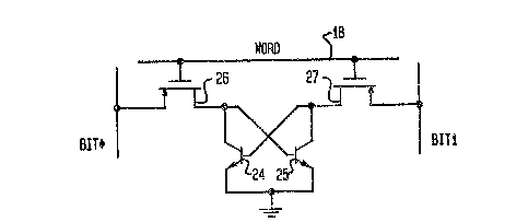
The particular ~ake-up of a ~emory cell constructed in
accordance with the present invention i8 schematically
illu6trated in Figure 2. A pair of cros~-coupled bipolar
transistor6 24, 25 form a bistable unit which stores one bit o~
data. Each transistor has its base connected to the collector of
the other transi~tor, ~nd the emitters of the two transistors are
connected in common. The two input/output ter~inals of the
bistable unit, formed by the common connection~ of the base and
collector termin~l~, are respectively connect~d to ~he bit lines
by mean~ of a palr of MOS transi6tor6 26, 27. ~n particular, ~he
~ource of each MOS transi~tor i8 conne~ted to one o~ the bit
lines, and the drain of the tran6i~tor ifi oonnected to one of the
input/output te~minals of the cross-coupled bipolar transistors.
5-
~ X a1 ~ 3 3 50.4380
The gate terminal6 of both MOS transistor6 are connected to theword line 18 for the row in which the memory cell i8 located.
The commonly connected emitters of the bipolar transistors
are preferably connected to a common potential for tha entire
memory circuit, e.g. ground, to thereby limit the number of
acces~ lines to three. If desired, however, ~ 6econd word line
can be provided for ~ach row of memory c~lls, and the emitters
can be connected to this ~econd word line.
In the operation of ~he ~2mory cell t the MOS devices
~unction in the non-~aturated region where the drain current
v~ries in proportion to the ~ource-to-drain ~oltaqe. In ~he
e~bodi~ent ~hown in Figure 2, ~he MOS transistors are p-channel
~PMOS) d~v~ces. Therefore, in the following description of the
operation of the circuit, ~ more po6itive gate voltage will
represent a lower drain current.
During the standby mode in which information i~ neither
written into nor read fro~ the circuit, 211 0~ the bit lines are
at the substanti~lly constant voltage V. All of the word lines
ar~ al80 at a rela~ivelY high voltage, e.g~ V VBIAs where VBIAS
i~ represented by the voltage of the variable ~eans 20 ~nd is a
low value. Accordingly, ~ach of the MOS transi~tor~ conducts
only A very small current from the power2d bit lines to ~he
blpolar tran6istor6 to maintain these transi~tors in a latched
state. For exa~ple, thi~ current can be in the neighborhood of
0.1 microamp.
Wh~n it i5 de~ired to read the information $n a cell, the
voltage of the word line connected to that cell iR lowered, for
example by increasing VBIAS under the control of the read/write
circuit 22. As a re6ult, the drain ourrent of one of the MOS
trans$stor6 in the cell will increa~e ~ubstantially. For
3 33 ` 50 . 4 3 8 0
example, if it iB a~umed that the memory cell is ~toring a logic
z2ro, the bipolar tr~nsi6tor 24 will be in a conductive state and
t~e transi6tor 25 will be non-conductive. Nhen the gate voltage
of the MOS transi~tor6 i6 lowered, the transistor ~6 wlll enable
a large current, e.g. 100 microamps, to flow on the BITO bit line
through the tran~istor 24 to ground. However, ~ince the
transistor 25 i~ non-conductive, the current in ~he BITl line
will remain low.
Aocordingly, a relatively large voltage will develop across
the re~iRtor 14 connected to the ~ITO line. This voltage can be
~ensed by any ~uitable ~e ns to d~tect the infor~ation stored in
the cell. For example, ~ di~ferential amplifier 28 can be
connected to the paix of bit line~ ln a colu~n. ~hen a read
operation ~ 6 performed, the voltage ~cross one of the resistors
14 will be much larger than the other. ~he a~plifier can sense
which bit line ha~ the larger current flowing through it, and
provide an output s$gnal ~ndicative o~ the value of the bit
stored ln the ~emory ~ell.
As an alternative, it i8 pD6~ible to momentarily raise the
voltage of ~11 of the other word lines during a read operation,
i.e. decrea~e VBIAS. Thi~ will have the effect of turning off
all of the ~emory cells except those ~ell6 ~onnected to the word
line who6e voltage i6 not raised. The r~lative currents can then
be examined in the two bit lines for the column in which the cell
of interest i~ located to determine the value of the bit stored
in the cell.
To perform a write operation, the voltag~ o~ all of the word
lines i6 rai~ed ~lightly to turn o~f the standby current. The
voltage of the word line for the eelected cell is lowered to a
level that i6 approxima~ely the ~ame as that for a read
-7-
~'~8~33 50.~380
Gperation. Then, the voltage of the appropriate bit line is
lowered. For example, if a logic one i~ to be written into the
cell shown in Figure 2, the voltage of the BITl line i6 lowered
by turning on its tran~istor 16 while at the 6ame time increasing
the effective resistance of it~ transi6tor 12 under control o~
the read/write circuit 22. A6 a result, current i~ drained ~rom
the cell ~hrough the MOS transi5tor 27 and injected through the
transi~tor 26. Thi6 di6turbance oP the cell will cause the
bipolar transi6tor 24 to be rendared non-conductive, while ~he
transistor 25 ~ turned on by the current being injected from the
~ITO line.
By u~ilizlng both bipolar ~nd MOS transi6tors to per~orm the
various functions in a 6tàtic memory cell, a numher of advantages
are obtained over cells which employ only one type of tran~istor.
More particularly, the bipolar 6witching transistors provide an
exponential change in output current relative ~o the input
voltage. Thu~, n ~mall change ln a word line g~te voltage to the
MOS tran6i6tors will produce a large current cbange in a bit line
and hence a large voltage acros6 the 6ense resistore 14, to
provide ~ more easily detectable read 6ignal with ~table
operation. On the other hand, the MOS coupling transistors
provide a bidirectional transmi6sion gate. Thus, during a write
operation the current can actually be pulled ou~ o~ a cell, as
opposed to merely turning o~f the base current to the 6witching
transi6tors. As a re~ult, a write operation cAn be per~ormed in
about 1/4 to 1/2 the ti~e that might be required i~ ~ipalar
coupling tran~i tors are employed.
Pr~ferably, the bipolar and MOS tran~istors that are
employed in ~he ~emory cell are of oppo~i~e conduc~ivity types,
i.2. PNP bipolar transi6tors in conjunction with n-channel MOS
-8-
~ 81~3~ 50.4380
tr~nsiætors or, more preferably, NPN bipolar with p-channel ~OS
transistor6~ This type of arrangement avoids the need to connect
the MOS transistors afi ~ource follower~, which could limit the
voltage ~wing av~ ble at the bases of the 6witching
transi~tors.
A~ a further feature o, ~he invention, the cell can be
con6tructed ~o that the ~OS transistors are stacked on top of the
~ipolar tr~ns~stor6. Accordingly, when the circuit i6
implement~d in a monolithic lC, each ~ell only requires the area
of two tran~i~tors.
One ~xample o~ the construction o~ 6uch a memory cell is
illustrated in Figures 3 and 4. In this example, p-channel MOS
~ran6istors are con~tructed on top o~ NPN bipolar transistors.
Referring fir6t to the bipolar transistor~, their co~mon emitters
are e~bodied in an n-type buried layer 30 for~ed on a grounded
substr~te 32. A p-type base layer 34 grown on top of the emitter
l~yer 30 i6 divided into two ~ctive portions ~y ~ield oxide 35
and an i~olation trench 36 to ~eparate the ~wo tran~i6tors. An
n-type ~ollector region 38 i8 diffused into e~ch of the two base
regions formed by the lay~r 34. Only one of these collector
regions iB shown in the cross-~ectional view o~ Figure 3. .The
~tructure 6hown in Figure 3 comprises an inverted transi~tor, in
that the collector i6 disposed at the top ~nd the emitter is at
the bottom.
The MOS tran6i~tors are ~mbodied ~n a recry~t~llized
poly6ilicon layer 40 that i6 di6po6ed on top of the bipolar
transi6tors and separated therefrom by ~ su$t~ble oxlde layer 42.
P-type diffusions 44 and 45 for~ the drain and 60urce regions of
the two ~OS transi6tor~, and an n-type diffusion 46 ~orms the
channel reyion. The ¢ro6s-coupli~g ~f ~ha bipolar transistors is
_g_
~xa~33 50.4380
provided by ~ans o~ Rilicided poly~ilicon layer~ sandwiched
between the MOS and bipolar transi~tors. One ~uch layer 47
c~nnect~ the collector 38 of one bipolar transi~tor to the base
reglon 34 of the other bipol~r transi6tor. In addition, ~he
embedded polysilicon 47 connecting layer i~ in contact with the
drain region 44 o~ one of the MOS transi~tor~. A similar la~er
48 displ~ced from ths l~yer 47 (~n a direction normal to the
plan~ of figure 3) connect~ the other ba~e, collector and drain
r~gion~ in a æimilar ~anner.
An oxide layer 50 i~ for~ed on top cf the r~cryst~llized
polysilicon 40 and provided with ~ r~ce6~ above the channel
region 46. A metal or silicided polysilicon conducting layer 52
i~ provided ~n this reces6 and for~5 the word line which i8
connected to all of the MOS tran~i~tor6 in a row. An insulating
layer 54, e.g. oxide, i6 depo6ited ~bove the word lines, and
met~l bit line~ 56 are ~orm2d on top of this layer. Contact
holes 58 are opened through the insulating layer 54 to ccnnect
the blt line~ to the ~our~e6 45 of the MOS tran~ietor6. The bit
lin~6 are diEpo6ed tran6v~r6e to the word lines 52 and connec~
all of the cell~ in a c~lu~n.
It will be appreciated by tho~e of ordinary ~kill in the art
that the pre6ent invention can be e~bodied in other ~peci~ic
for~s without departing from the ~pirit or e66ential
characteri6tics thereof. For example, the ~OS and b~pol~r
tra~istors c~n be con~tructed in a side-by-~ide ~rr~nge~ent if
the square area per cell does not need to be minimized. The
presently di~closed e~bodi3ent i6 ~herefor~ consid0red in all
respect~ to be illu6trative and not re~trictive. ~he ~cope of
the invention i~ indic~ted by the appendsd clai~ rather than the
foregoing de~cription, a~d all change~ that come within khe
--10--
33
50 . 43BO
meaning ~nd range of equiv~lent~ thereo~ ~re intended to be
e~braced therein.