Note: Descriptions are shown in the official language in which they were submitted.
~2 8~1~4 FJ-6535
MULTIPLEXING APPARATUS HAVING BSI-~ODE PROCESSING
.. , ... .. . . . . . .. _ . _ _ .. . . . .
AND BIT INTER~EAVE FUNCTIONS
BACKGROUND OF THE INVENTION
1. Field of the Invention
The present invention relates to a multi-
plexing apparatus having a BSI-code processing function
and a bit interleave function.
In a digital transmission system using optical
fibers, etc., a reliable transmission of all kinds of
information signals must be guaranteed. To ensure this
transmission reliability, a Clear Channel Capability is
required in which timing clock signals can be stably
extracted from the input information signals without
generating code errors, even when the input information
signals include consecutive "0"s or "l"s, i.e., direct
current components. To realize the Clear Channel
Capability, the codes on transmission lines must be
bit-sequence independent (BSI).
On the other hand, in a time division multi-
plex system, a digital hierarchy including many gxoups
from the lowest-order group to the highest-order group
has been developed. In addition, attempts have been
made to develop a synchronous multiplex system which can
realize a multiplex transmission without inserting, at
each multiplexing process in each multiplexing circuit
in each group, control signals such as frame synchronous
signals, so that the increase of the transmission speed
due to the insertion of the control signals is not
caused after each multiplexing process. By this sys~em,
the transmission speed in each multiplexing circuit is,
therefore, an integer multiple of a basic PCM signal
speed, and thus in each multiplexing circuit, signal
processing can be carried out only under the control of
the basic clock signal.
To realize the above described synchronous
~i
~L~81~4~
-- 2
multiplex system, PCM signals having a basic signal
transmission speed are given with frame structures
provided with multiplexing control signals such as frame
synchronous signals and channel numbers of channels to
be multiplexed By this frame structure, the signal
speed after the multiplexing is made an lnteger multiple
of the basic PCM signal speed. Thus, a synchronous
multiplexing system, which is different from conven-
tional stuffing, is realized. The synchronous multi-
plexing technique, however, has been devised whiletaking only the multiplexing system into account, and,
therefore, is not satisfactory as a ~ransmission system
with the clear channel capability. Namely, no consid-
eration has been given in the synchronous multiplexing
system to realizing the BSI of transmission line codes.
Therefore, there is a need for a constitution which
takes into account the BSI of the transmission system as
well as the synchronous multiplexing system.
2. Description of the Related Art
Conventionally, the BSI process of digital
transmission codes is realized in a transmission
terminal equipment, and a time division multiplexing
process, etc., is usually carried out in a multiplexing
unit. For this, a signal speed of the PCM hierarchy is
used as an interfacing speed between the time division
multiplexing process and the transmission terminal
equipment. Accordingly, the transmission terminaI
e~uipment which receives multiplexed PCM signals must
carry out a speed conversion of the PCM signals by
executing the BSI process such as an 8BlC (8th~bit
one-complement by which one block becomes 9 bits) or a
5B6B (5th-bit 6-bit by which one block becomes 6 bits)
and transmit the speed-converted signals to a trans-
mission line. Further, at a receiving station, the
signals are subjected to a reverse BSI process, a speed
conversion process and a demodulating process, and
transmitted to a multiplex converter. In this way, the
-- 3 --
BSI process is executed within the transmission terminal
equipment, as later described in more detail with
reference to the drawings.
As described above, in a conventional digital
S multiplex transmission system, the multiplexing system
and the transmission system (BSI, etc.,) are provided
separately. Therefore, even if a frame constitution
which is adequate for the multiplexing system is adopted,
that is, even if information signals with a basic PCM
signal speed are provided in advance with a frame
constitution to which control signals such as frame
synchronous signals and channel numbers of channels to
be multiplexed are added for the synchronous multi-
plexing and demultiplexing processes, the transmission
terminal equipment treats these control signals and
frame synchronous signals only as information signals.
The conventional BSI process, such as a BSI bit inser-
tion and removal, necessary for the transmission system,
is carried out in each transmission terminal equipment.
Therefore, in each transmission equipment, the multi-
plexed signal having a regularized speed of, for
example, an integer multiple o the basic PCM signal
speed, must be converted into a signal with the BSI
having an increased speed. Because of the speed
conversion, the advantage of the multiplexing system of
the digital hierarchy utilizing the basic PCM signal
speed is lost in the transmission equipment. Further,
due to the necessity of the speed conversion, the
hardware scale of the transmission equipment becomes
large and expensive.
SUMM~RY OF THE INVENTION
An object of the present invention is to provide a
multiplexing apparatus having a BSI-code processing
function and a bit interleave function in which the
advantage of the synchronous multiplex system is
maintained.
Another object of the present invention is to
~81~4~
provide the above multiplexing appal~atus in which each
unit has no speed conversion part.
Still another object of the present invention is to
provide the above multiplexing apparatus-in which a
small-scale transmission equipment is provided.
A still further object of the present invention is
to provide the above multiplexing apparatus in which the
transmission equipment is provided at a low cost.
To attain the above objects, there is provided,
accoraing to the present invention, a multiplex}ng
apparatus of a bit interleave type for time-division
multiplex on PCM signals of a plurality of channels bit
by bit to convert said PCM signals into a high-speed PCM
signal. The multiplexing apparatus has a BSI-code
processing function and a bit interleave function, and
comprises: a BSI-code adding means for adding BSI codes
to the PCM signals before multiplexing; a BSI-code
posi~ion shifting means for shifting the positions of
the BSI codes in the PCM signals to different positions
respectively with respect to the PCM signals of a
plurality of channels; and a multiplexing means for
multiplexing the outputs of the BSI-code position
shifting means by a bit-interleave mode.
According to another aspect of the present inven-
tion, there is provided a multiplexing apparatus of abit interleave type for time-division multiplex on PCM
signals of a plurality of channels bit by bit to convert
the PCM signals into a high-speed PCM signal; the
multiplexing apparatus having a BSI-code processing
function and a bit interleave function~ BSI bits being
inserted into each predetermined block of input PCM
signals in advance, and comprising: basic PCM signal
channel processing portion each for shifting positions
of said BSI bits of said respective channels and for
multiplexing the shifted bits with the PCM signals of
corresponding channel.
The outputs of the basic PCM signal channel
-- 5
processing portions are multiplexed under a bit inter-
leave mode. The multiplexed signals are inverted at the
BSI bits.
According to still another aspect of the present
invention, there is provided a multi~lexing apparatus oE
a bit interleave type for time-division multiplex on PCM
signals of a plurality of channels bit by bit to convert
the PCM signals into a high-speed PCM signal, the
multiplexing apparatus having a BSI-code processing
function and a bit interleave function, and comprising:
a BSI-code adding means for adding BSI codes to the PCM
signals before multiplexing; a basic PCM signal channel
processing means; and a multiplexing portion.
The basic PCM signal channel processing means
includes separating means for separating a frame control
signal, a BSI code, and data, included in each frame of
the input PCM signals; a memory for temporaxily buffer-
ing the data; frame control means changing the channel
number in the frame control signal; BSI-code shifting
means for shifting the BSI code; multiplexing means for
multiplexing data read from the memory, the frame
control signal, and the BSI code; and a multiplexing
portion comprising bit interleave multiplexing means for
multiplexing a bit sequence input from the PCM signals
of a plurality of channels.
BRIEF DESCRIPTION OF THE DRAWINGS
The above objects and features of the present
invention will be more clearly understood from the
following description of the preferred embodiments with
reference to the drawings wherein:
Fig. 1 is a view showing a data format of a
PCM channel utilized in the present invention;
Fig. 2 is an explanatory view showing a
principle of the present invention;
Fig. 3 is a view showing the constitution of
an embodiment of the present invention;
Fig. 4 is a view showing the constitution of
~81~
-- 6 --
another embodiment of the present invention;
Fig. 5 is an explanatory view showing an
effect of the present invention;
Fig. 6 is a view showing the constitution of a
prior art; and
Fig. 7 i5 a view showing an example of a frame
constitution subjected to a BSI process.
DESCRIPTION OF THE PREFERRED EMBODIMENTS
For a better understanding of the present inven-
tion, a conventional BSI bit interleave multiplex systemwill first be described with reference to Figs. 6 and 7.
Figure 6 is a block diagram showing a conventional
BSI bit interleave multiplex system.
In the figure, 1 represents a multiplex converter,
and 2 represents a transmission terminal equipment. The
multiplex converter 1 multiplexes input signals C~l to
CHn of "n" channels to supply a signal of ~n x fo + a)
bps to the transmission terminal equipment 2, and
further, supplies a clock of (n x fo + a) Hz corres-
2~ ponding to the signal. The "a" bits are those allocatedfor a frame control signal in each frame. In the
transmission terminal equipment 2, the multiplexed
signal is subjected to a serial/parallel (S/P) conver-
sion, a buffering, and a parallel/serial (P/S) conver-
sion and output. During this process, by using a speedconverting circuit 2a having a PLL circuit, a block of
8 bits is converted into a block of 9 bits by inserting
a BSI bit.
Figure 7 is a view showing the converting process
to the 9 bits. The multiplexed signal is divided into
segments each having 8 bits. For example, an 8th bit #8
in one block is inverted to #8 and added to the block.
The signal is then sent as a multiplexed transmission
signal.
With the constitution shown in Fig. 6, a speed of
the transmission signal is increased due to the inser-
tion of the BSI. Therefore, the advantage of the
1~8~
-- 7
synchronous multiplexing system, that is, the trans-
mission speed after the multiplexing becomes an integer
multiple of the basic PCM signal speed so that the
interface speed and multiplexing unit are simplified, is
not effectively utilized in the conventional trans-
mission equipment.
Now, embodiments of the present invention will be
described.
Figure 1 is a view showing a data format of a PCM
channel which is utilized in a multiplexing apparatus
according to the present invention. In the figure, a
PCM signal of a channel CHi before multiplexing includes
a sequence of frames each consisting of a frame synchro-
nizing signal F, a channel number ID, and an information
payload tdata) IP. In the informa~ion payload IP, a BSI
bit is inserted after, for example, each 8-th bit of one
block, as shown in Fig. 2.
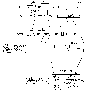
Figure 2 is an explanatory view showing the princi-
ple of the present invention. In the figure, informa-
tion payload IP in each channel is divided into a number
of blocks. A BSI bit is added to, for example, each
block in each of the channels CHl to CHm before multi-
plexing. The BSI bits may be added before input to the
multiplexing apparatus. Alternatively, the BSI bits may
be added at the input stage of the multiplexing appara-
tus. After adding the BSI bits, each BSI bit in achannel CHi is shifted by "i x k" bits from the origi--
nally added position. For example, each BSI bit in the
channel CH2 is shifted by "k" bits. Also, each BSI bit
in the channel CHm is shifted by "m x k" bits. Alterna-
tively, each block including a BSI bit may be entirelyshifted by k bits. This alternative method, however,
causes a delay of the information payload, i.e., data,
by k bits~ and it is preferable not to delay the infor-
mation payload. To cope with this, in the figure, theinformation payload (IP) is not delayed but only the BSI
bits are delayed by X bits. Note, the positions of the
-- 8 --
shifted BSI bits are determined by the channel numbers
and the predetermined number "k". The shift of the BSI
bits is necessary in order to avoid a continuous series
of BSI bits after multiplexing. Since the positions of
the BSI bits shifted in each channel can be identified
by counting the bit length from the frame control siynal
in the channel, phases of blocks o~ the respective
channels need not be aligned, although they are aligned
in the figure for easy understanding.
1~ The channels CHl to CHm with the shifted BSI bits
are then multiplexed by a bit interleave method.
As the BSI bit, a differential 8BlM (8-bit one
mark~ as illustrated in the figure is used as an
example. By the differential 8BlM (D8BlM), a mark M is
added to a position corresponding to a 9th bit in each
block, and when the mark M is found by a receiver, a
bit #8 is inverted to #8', and inserted into the 9th
bit. Thus, a new one block consisting of nine bits #1,
..., #8, and #8 is formed. The D.C. components in the
PCM signals can be removed by the differential coding.
In place of the D8BlM, 8BlC may be alternatively
used as the BSI bit. By the 8BlC, the 9th bit in each
block is always an inverted signal of the 8th bit.
Therefore, after multiplexing of m channels, ~n inverted
signal appears in at longest m x k bits so that the BSI
is satisfied, although it is not sufficient.
In operation, basic PCM signals are made to have
BSI bits when their frames are formed. To multiplex the
basic PCM signals with the BSI bits, positions of the
BSI bits are shifted according to channel numbers of
channels to be multiplexed. Therefore, the BSI bit
inserting process can be realized without processing
high-speed PCM signals after multiplexing. As a result,
the transmission e~uipment can be simplified and
realized in compact sizes while satisfying features of
the synchronous multiplex system. Accordingly, clocks
in a transmission switching network can be simplified,
L4~
and multiplexing circuits can be formed in modules so as
to reduce the C05t.
Figure 3 is a block diagram showing the constitu-
tion of a multiplexing apparatus according to an embodi-
ment of the present invention. In the figure, areference numeral 10 represents a multiplexing portion
corresponding to the conventional multiplex converter 1
shown in Fig. 6. Reference numerals 11-1, 11~2, ...
ll-m represent basic PCM signal channel processing
portions provided to correspond to respective channels
for carrying out a preparatory process corresponding to
the multiplexing process shown in Fig. 1. A numeral 12
represents a frame control signal and BSI bit separating
portion which separates information signals (IP), frame
control signals and BSI bits one from another. A
numeral 13 represents a frame synchronization portion
for effecting frame synchronization of input signals and
generating timing signals necessary for respective
circuits. A numeral 14 represents an elastic store for
adjusting a time for writing or reading information
signals. A numeral 15 is a frame controlling portion
for updating multiplexing overheads of, for example,
channel numbers of channels to be mul~iplexed included
in the frame control signals. A numeral 16 is a BSI bit
shifting portion for shifting positions of BSI bits so
as to satisfy the condition that each block in each
channel includes at least one BSI bit after multi-
plexing. A numeral 17 is a multiplexing controlling
portion for generating frame signals and providing phase
adjusting instructions with respect to multiplexing
reference phases, according to instructions from a
multiplexing channel controlling circuit 19. A numer-
al 18 is a differential coding portion for differential-
coding ("1": inverting data; "0": holding data of a
previous time slot) multiplexed signals from the
respective channel processing portions (11-1 to ll~m).
A numeral 19 is the multiplexing channel controllin~
-- 10 --
circuit for generating reference frames necessary for
the multiplexing process and instructing channel numbers
of the respective channel processing portions. A
numeral 20 is a bit interleave multiplexing circuit for
performing a bit interleave multiplexing.
Numerals 22-1, 22-2, ..., and 22-m are BSI-code
adding circuits for adding BSI codes to the input basic
PCM signals.
In operation, a basic PCM signal of each channel is
subject to BSI process in the BSI-code adding circuit
22-1, 22-2, ... or 22-m. The basic PCM signal after the
BSI process is input to the frame control signal and BSI
bit separating portion 12 wherein frame control signals
and BSI bits are separated from the PCM signal (informa-
tion payload) and input to the frame controlling por-
tion 15 and the BSI bit shifting portion 16, respec-
tively. Information payloads (data) are input to the
elastic store 14. In the BSI bit shifting portion 16,
the BSI bits are shifted in advance so that a trans-
mission signal may have the BSI characteristic. Accord-
ing to a control signal from the multiplexing channel
controlling circuit 19, the multiplexing controlling
portion 17 generates frame signals and provided
instructions with respect to multiplexing phases.
Accordingly, the multiplexing circuit 21 multiplexes the
data, frame signals and BSI bits.
Signals of respective channels multiplexed in this
way are input to the bit interleave multiplexing
circuit 20 in which the signals are multiplexed for each
3a bit under a bit interleave mode. The multiplexed
signals are differential-coded in the differential-coding
portion 18 and transmitted.
The BSI-code adding circuits 22-1 to 22-m at the
input stage of the multiplexing apparatus as shown in
Fig. 3 may be omitted and the BSI bits may be added at a
transmitting side (not shown in the figure). In this
case, the BSI bits are already included in the input
~8~4~
basic PCM signals.
Figure 4 shows another embodiment of the present
invention. In the figure, the multiplexing apparatus
according to the another embodiment of the ~nvention
includes BSI-code adding circuits 22-la, 22-2a, ... and
22-ma, basic signal channel processing portions ll-la,
11-2a, ..., and ll-ma, and a multiplexing portion lOa.
The sSI-code adding circuits 22-la, 22-2a, ... and 22-ma
are the same as those of Fig. 3. Each of the basic
signal channel processing portions ll-la, 11-2a, ....
and ll-ma includes a shift register ~SR) 16a and a
selector (SEL) 21a. The multiplexing portion lOa
includes a bit interleave multiplexing circuit 20a and a
multiplexing channel controlling circuit 19a. The
selectors (SEL) 21a are controlled by the multiplexing
channel controlling circuit l9a.
In operation, the basic PCM signal in each channel
after the BSI processing by the corresponding BSI-code
adding circuit is shifted bit by bit in the shift
register 16a. Then, the selector (SEL) 21a selects,
under the control of the multiplexing controlling
circuit 19a, the necessary outputs from the outputs Ql
to Qn of the register 16a. A one block of, for example,
9 bits is selected at one time. The selected block is
determined in accordance with the channel number. Thus,
at the output of the selector 21a, the entirely shifted
PCM signal of one block is obtained and the shifted
value is determined in accordance with the channel
number. The outputs of the selectors 21a in all of the
basic PCM signal processing portions ll-la to ll-ma are
multiplexed under the bit interleave made by the bit
interleave multiplexing circuit 20a. The multiplexed
signal is output to the outgoing line.
According to the above embodiment, not only the BSI
bit but also the information payload is shi~ted. It is
not difficult to discriminate the information payload by
providing a necessary discriminating circuit, although
~.~81~4~
- 12 -
it is not preferable to shift the information payload.
In this embodiment also, since the BSI bits are shifted
before multiplexing, the effect of the present invention
is also obtained.
Figure 5 is an explanatory view showing an experi-
mental effect of the differential 8BlM used for the BSI
process. In the figure, an abscissa represents the
number of channels to be multiplexed, and a dotted line
showing how to select, according to the number of
channels, the shifting quantity "k" explained with
reference to Fig. 2. A continuous line shows, in the
worst case, how many bits of the same codes continue
with respect to a given optimum shift value "k".
Naturally, the BSI bits are inserted to prevent the same
code from appearing consecutively.
As will be understood from Fig. 5, the same codes
continue only between 9 bits and 11 bits, when the shift
value "k" is selected as shown in the dotted curve.
From the foregoing description, it will be apparent
that, according to the present invention, since basic
PCM signals have BSI characteristics with no further
processes on high-speed PCM signals after multiplica-
tion, the transmission equipment can be simplified and
the size thereof minimized. Further, the features of a
synchronous multiplexing system can be simultaneously
provided in a satisfactory manner. In addition, clocks
of a transmission switching network can be simplified,
and multiplexing circuits can be formed in modules tc
reduce the cost.