Note: Descriptions are shown in the official language in which they were submitted.
1.2~ 19
EVANESCENT
WA~E SENSORS
Technical Field
The present invention relates to a novel evanescent
wave sensor which can have a high numerical aperture and
is capable of being used in various forms of optically-
based assays. Unlike previous fiber optical devices, the
present sensors do not use any cladding at the contact
points.
Description of the ~rawings
Figure 1 is a cross-sectional view of the seal of
the present sensor.
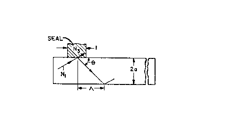
Figure 2 is a cross-sectional view of the present
sensor showing the angle Theta (~).
Figure 3 is a cross sectional view of a preferred
form of the present sensor.
Figure 4 is a diagram of an optical system for use
with the present sensor.
Figure 5 is a graph comparing the sensitivity of the
present sensor versus conventional solution fluorimetry.
Figure 6 is a graph showing a fluoroimmunoassay
performed with the present sensor.
Backqround Art
The use of evanescent wave phenomena as a detection
means in optically-based assays is known in the art. The
total reflective spectroscopy (TRS) techni~ues of Myron
Block (U.S. 4,447,546 and U.S. 4,558,014) use an
evanescent wave to both excite a fluorescently tagged
analyte and to detect the resulting fluorescence. As
disclosed therein, the sensors are comprised of optical
telecommunication-type fibers which have a core
surrounded by a cladding, at least where the fiber is
held. Another portion of the fiber has a bare (or naked)
~81;~9
- 2 -
core which is coated with an immunochemically reactive
substance, i.e., an antigen or an antibody. This basic
sensor configuration can be found in other disclosures
such as WO 83/01112 to T. Carter et.al. and U.S. Serial
No. 652,714 to D. Keck et.al., now U.S. Patent Number
4,880,752 tissued November 14, 1989).
The presence of a cladding or means to insure energy
isolation has both positive and negative effects. On the
positive side, the cladding prevents mode stripping where
the fiber is held. This is especially important when one
is using a sensor for evanescent wave detection because
in some cases, i.e., fluorescent measurements, less than
one percent of the excitation energy will return as a
signal. Thus, cladding has been required to insure that
signal stripping does not occur. However, the negative
consequences of this approach include manufacturing
difficulties in selectively stripping or adding cladding
to a fiber and the inherent limitation the cladding
imposes on the critical angle or numerical aperture (NA)
of the sensor.
The critical angle ec of a fiber optic or waveguide
device, in general, and an evanescent wave sensor, in
particular, is determined by the differences between the
refractive indices of the launching medium, propagating
medium, and the surrounding medium. It refers to the
maximum angle, with respect to the longitudinal axis of
the waveguide, at which light can enter the waveguide and
still be retained and propagated by the waveguide. In
practice, the art refers more often to the numerical
aperture (NA) of a waveguide rather than the critical
angle. Mathematically, the relationship is as follows:
NA= No sin ec = (N1 - N2 )
Where No = refractive index of the launching medium
-- 3
N1 = refractive index of the propagating
medium
N2 ~~ refractive index of the surrounding
medium.
(See Figure 1).
Disclosure of the Invention
The present invention relates to evanescent wave
sensors that are useful in optically-detectable assays,
including such formats as immunoassays, enzymatic
clinical chemistry assays, molecular probe hybridization
assays, cell measurements, and dye-based pH/blood gas
assays. However, the use of these sensors is not limited
to aqueous solutions, but rather can be used in gaseous
or non-aqueous environments. The labels or tags for
these assays include fluorescent, chemiluminescent, and
absorptive compounds well known in the art.
The sensor is comprised of two parts, a light
conducting means and a holding means. The former is a
electromagnetic wave-propagating device of numerous
configurations; e.q., cylindrical or planar.
Functionally, it carries light along the waveguide to a
point where the propagating surface of the waveguide
(and, of course, the accompanying evanescent wave)
contacts optically-detectable or labelled analyte.
The unexpected novelty of the present sensor lies in
the use of a holding means wh.ich can contact the light
conducting member at the wave-propagating surface, erqo,
the latter does not require a conventional cladding or
energy isolation means attached thereto where it is held.
The holding means contacts the wave-propagating surface.
There are three general cases, one of which is thickness
dependent.
In cases where the seal material is optically
~312~9
-- 4 --
transmissive and has an index of refraction (N3) which is
greater than that of the medium surrounding the light
conducting member, mode stripping, i.e., the loss of
transmitted light due to contact pertubation, is
minimized by controlling the thickness at the contact
points. The thickness of the contact points should be
less than Lambda (A) divided by the optical parameter
(f), where A equals the cross-sectional thickness of the
light conducting member divided by the tangent of the
propagation angle theta (9). Theta is less than or equal
to the critical angle of the light conducting member, as
shown by comparing Figures 1 and 2, and f is a material-
dependent parameter associated with the light
transmission across the waveguide/seal interface which
varies between one and zero.
Optical power loss in seals can be independent of
thickness in cases where either the seal or the contact
surfaces of the light conducting member are made of
either optically-transmissive or optically reflective
materials. In the former case, the seal is made of a
material having an index of refraction less than both the
light conducting member and the medium to be sampled.
While in the latter case the seal or the light conducting
member has a reflective surface at the interface between
the two.
Without conventional types of cladding, the NA of
these sensors becomes dependent on the difference between
the refractive indices of the light conducting member and
the surrounding medium, e.g., air or water. Thus, for
aqueous-based assays the high end of the sensor NA range
is no longer restricted to about 0.3, but can now be
extended to 0.6.
The combination of easier manufacturing requirements
and expanded capabilities makes the present invention the
evanescent wave sensor of choice. Conventional cladding
1~81~9
steps are eliminated, and greater NA's mean substantially
greater sensor sensitivity. It has been determined
experimentally (at sin ~max) that the fluorescent signal
associated with free fluoresc~in varies strongly,
approximately equal to sin8 ~max~ where ~max is the
maximum angle for light launched into the light
conducting member.
Preferred Modes of the Invention
The present sensor can be made from a wide selection
of materials. Optical glass and plastic are preferred
for the light conducting member. The choice can be based
on the selected excitation and detection wavelengths, and
possible absorption or internal fluorescence
interferences at those wavelengths. It should be noted
that for the present purposes, "light" also refers to
wavelengths outside of the visible spectrum, including
the ultraviolet and infrared ranges.
Likewise, the holding means can be made from a
variety of materials, however, the choice of material
affects the required thickness at the contact points for
minimal optical pertubation. The optical transmission of
light (T) within the light conducting member is given by
the following formula:
T = 1-(tf)/A
where t is the seal thickness, and T varies between zero
and one.
Depending upon the relative magnitudes of Nl, N2,
and N3, (N3 being the refractive index of the seal),
several cases can be generated:
~ 9
- TABLE I
CaseTransm~ss~on Conditions Requirements for
Min~mum Power
~ _ .
Loss
1 T-l f=O Nl~N2>N3 t is not
functional
2O~T~l O<f~l Nl>N3~N2 (t/~f~<l
3-O~T~l f=l N3=Nl>N2 (t/~)~l
3 Nl N2 (t/~)f<~l
T~1 f~O Nl>N2 t is essentially
not functional
In the first case of Table I, t is not functional~ and
thus, the thickness of the seal becomes essentially
immaterial because the seal maintains the electromagnetic
radiation within the light conducting member. In practice,
one selects a seal material having an index of refraction
lesser than or equal to that of the surrounding medium. The
remaining cases probably have greater utility because one
selects the seal material with respect to the material used
for the light conducting member, and thus, typically, a
greater selection of materials is available. In the second
case, a polyfluorinated hydrocarbon seal (such as Teflon ~)
would be used on a light conducting member which is made of
optical glass and which is surrounded by an aqueous
solution. Such a seal is preferred because the ref active
index of the Teflon~ closely matches that of the aqueous
solution.
~ 9
If other materials such as latex or the light
conducting material itself ~ere to be used for seals, and
thus N3 ~s greater than or equal to N2,the~ the th~ckness o~
the seals would have to be lim~ted to the conditions set
forth in the third and fourth cases ln Table I. For
example, where a rubber seal is used on a light conducting
member made of optical glass, the power loss-is strongly
dependent upon the thickness of the seal.
Finally, the last case in Table I refers to sensors
wherein f approaches zero, as in the first case. However,
t~e selection of the seal material is no longer based on
indices of refraction. Here, the seal is reflective but not
optically transmissive. For example, the seal contact
surface comprises a mirror-like coating. The coating having
been deposited on either the seal surface or the contact
surface of the light conducting member.
The shape Qf the sensor elements is not restricted to
one configuration. The light conducting member may be
either a solid or hollow, cylindrical or planar surface
having any desired thickness. Unlike prior
telecommunication fiber sensors, thickness can easily exceed
lOOO microns. Likewise the holding means can be suited to
both the light conducting member and any associated sensor
structures such as protective or sample volume shields,
locking means, et al. Of course, the key feature is that
the contact points thickness does not exceed the above
limits. The points can be distinct or merged into a
gripping flan~3e ring.
Preferably the holding means contacts the light
conducting member within a set distance (x) from the
electromagnetic radiation launching end of the member. This
reduces the pertubation effect of the seal when the launched
light spot is smaller than the cross section of the light
1X 8~ 3
conducting member. Mathematically this d~stance ~s defined
as
x =(Rf - Rs)/tan~
where:
Rf = one half of the cross-sectional thickness of
the member;
Rs = one half of the cross-sectional thickness of
the launched optical spot (Rf> Rs); and
~ ~ = angle theta ~as described above).
In practice, a typical immunoassay sensor would be
configured as shown in F~ e 3. A sensor (10) comprises a
light conducting member or waveguide (12) made of optical
glass (n = 1.46) and having diameter of 500 microns and a
length of 7 cm. Placed about the fiber is a tubular sample
chamber (14) ha!~ing inlet and outlet means (16) of greater
diameter and lesser length (5 cm.). Alternatively, the
sample chamber can be greater in length with a recessed
fiber, the caps extending inwardly to grip the fiber. The
holding means is comprised of molded end caps (18) made from
Teflon (n = 1.34) which are designed and shaped to grip the
chamber end, forming a watertight seal, and to contact
circumferentially the light conducting member with a thin
contact distance for minimal pertubation. (See Table I).
Those slcilled in the art recognize the wide
applications of such sensors. For example~ IR or UV
absorption of the evanescent wave can yield identification
and concentratlon of many organic liquids, the sensor
serving as a monitor for chemical process control.
The effect of excessively thick contact points can be
readily seen as follows, where the observed fluorescent
slgnal decreases from 900 to 51 rps with an increase in seal
~hickness o~ 0.14 to 2~00 mm.:
Table II
EVANESCFNT WAVE 5ENSOR SEAL MATERIALS
Rubber Latex Teflon~
__. __ ____
Refractive Index 1.51 1.51 1.34
Seal Thickness ~mm) 2,00 0.14 0.25
Fluorescent signal (cps) 51 900 8000
The use of both a low-index material such as Teflon~,
and thin contact distance gives an extremely well-optimized
signal. (The above results have been obtained using an
aqueous solution of fluorescein at 10-6 molar.)
The use 'of the present evanescent wave sensor is
illustrated by the two examples described below both of
which used an optical system as shown in Fi~ure 4.
Solution Fluo_imetry
In Figure 5, aqueous solutions containing various
concentrations of fluorescein isothiocyanate (FITC) were
placed in the sampling chamber surrounding a fiber. Using
490nnl excitation light and detecting 525nm fluorescent
emission as cps with a photon counter, the relation between
fluorescent signal and FITC concentration was,established.
This is shown to correspond well with the fluorescence
versus concentration curve observed with a commercial
conventional solution cuvette fluorimeter (Perkin Elmer
Model 650-40).
~ 8
Immumoassay
In Figure 6, a fluor~meteric immunoassay was
constructed for -the cllnica~ly relevant analyte ferritin
usin~ fiber sensors in which the ~lass fiber component had
been previously coupled to anti-ferritin antibodies through
the art described in (Weetall Paten~ U.S. 3,65~,271-). The
sensors were then incubated with various concentrations of
ferritin (to produce an immunological binding reaction),
washed, then incubated with a secondary ferritin antibody
which was labelled with FITC. The proportion of bound
labelled antibody gave rise to an increased level of
fluorescent signal (as expressed in cps), which is
proportional to the amount of ferritin in a sample. The
assay range is of clinical relevance while the assay could
be performed in 20 minutes or less.
It should be apparent to one having ordinary skill in
the art that ma,iy variations are possible without departing
from the spirit and scope of the invention.