Note: Descriptions are shown in the official language in which they were submitted.
~2~ g
The present invention relates generally to communication
systems for transmitting and receiving data in conjunction with a
broadcast television signal and more particularly concerns the
transmission and reception of data in subscription television
systems.
This application is related to applicant's copending
application serial no. 503,953 entitled 'Television Signal
Scrambling System', filed March 12, 1986.
The subscription television systems, television signals
are typically transmitted to system subscribers in a scrambled
form either along a coaxial cable or as an 'over-~he-air' broadcast.
Each system subscriber is provided with a decoder operable for un-
scrambling the transmitted television signal and for supplying the
unscrambled signal to a conventional television receiver for
viewing. In addition, many present-day subscription television
systems are addressable in nature whereby the operation of indivi-
dual decoders may be selectively controlled through the transmission
of system control data generated at the system head-end. The
system control data may include such information as subscriber
address codes, subscriber authorization codes, program codes and
the like enabling the system operator to designate different levels
or tiers of programming authorized for different individual
subscribers.
Various techniques are known in the industry for trans-
mitting such system control data in conjunction witha television
;, signal. These known techniques, however, are normally limited in
the amount of data which can be transmitted in a reasonable time
~28~
frame and typically require the use of relatively complex and
therefore expensive data encoding and decoding apparatus.
0 ects of the Invention_
It is therefore a feature of the present invention to
provide an improved technique for.transmitting data in con-
junction with a scrambled broadcast television signal.
It is a more specific feature of the invention to
provide a subscription television data transmission system
capable of transmitting relatively large amounts of data in
conjunction with a broadcast television signal yet requiring
the use of relatively non-complex and inexpensive data encoding
and decoding apparatus.
Specifically, the invention relates to a combination
television signal encoding the data transmission system com-
prising: means for developing an RF television signal includ-
ing an amplitude modulated RF video component and a frequency
modulated RF audio component; means for defining a plurality of
encoding intervals, each characteri~ed by at least a first or a
second predetermined characteristic respectively respecting
dlfferent states of a data bit, each of the encoding intervals
corresponding to at least a portion of a respective horizontal
blanking interval of said RF television signal; means for
encoding the RF television signal during the encoding intervals
according to a predetermined function; means for transmitting
the encoded RF television signal; means for receiving the trans-
mitted signal; detection means responsive to the received signal
for detecting the encoding intervals and having a characteristic
complementary to the predetermined function for decoding the
RF television signal; and means responsive to the first and
. ~ ~ ...................... .
the second predetermined characteristics for determining the
state of the data bit represented by the decoding interval.
BRIEF _ESCRIPTION OF THE DRAWINGS
Features of the invention which are believed to be
novel are set forth with particularity in the appended claims.
The invention, together with its ob;ects and the advantages
thereof, may best be understood by reference to the following
description taken in conjunction with the accompanying drawings
in which:
Figure 1 is a block diagram of a television signal
transmitter according to the invention;
Figures 2A and 2B are waveform diagrams illustrating
a standard NTSC RF television signal and the detected video
envelope thereof;
Figures 3A-3B and 4A-4B are waveform diagrams illus-
trating the manner in which the NTSC signal of Figure 2A is
modified according to the invention and the corresponding
, control signals produced in response thereto;
pg/~ 2A -
f ., ~ ,.
~IL;2~
Figures 5A-5B and 6A-6B illustrate the amplitude and
normalized phase versus frequency response characteristics of the
SAW Filters utilized in the transnitter and receiver of the
invention;
Figure 7 is a block diagram showing a decoder operable
in response to transmitted data of the type represented in
Figures 3A and 4A; and
Figures 8 and ~ are block diagrams of alternate
embodiments of the transmitter and decoder of the invention.
: 10 Detailed DescriPtion of the Preferred Embodiment
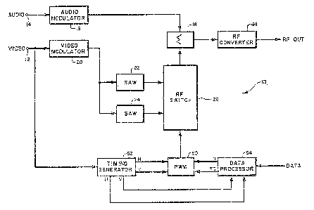
Referring now to the drawings, Figure 1 is a simplified
block diagram illustrating a headend television signal scrambler
and data encoder 10 according to the present invention. It will
be understood that the signals provided by scrambler and data
:15 encoder 10 are intended to be broadcast for transmission through
a suitable medium such as a coaxial cable in a CATV system for
reception by the system subscribers. Each system subscriber is
: provided with a decoder which may be authori~ed for unscrambling
a particular broadcast television program in response to data
signals received from headend unit 10. Thus, with relation to a
particular television program, an authorized subscriber will be
provided with an unscrambled video image for viewing while all
unauthorized parties, whether system subscribers or not, will be
provided with a television signal producing a scrambled video
image which is largely unintelligible when displayed on a
conventional television receiver viewing screen.
With more particular reference to Figure 1, a.
conventional NTSC composite baseband video signal is coupled to
an input terminal 12 of headend unit 10 with the associated audio
baseband signal being applied to an :input terminal 14. The audio
baseband signal is coupled to an audio modulator 16 where it is
used to frequency modulate a sound intermediate frequency (IF)
L4~
carrier, typically 41.25 MHz, which is then applied to one input
of a summing circuit 18. The composite baseband video signal is
coupled to a video modulator 20 where it is used to amplitude
modulate a video IF carrier spaced 4.5 MHz from the sound IF
carrier, i.e., 45.75 MHz. The IF video signal developed at the
output of modulator 20 is applied to the inputs of a pair of
filters which, in a preferred embodiment of the invention,
comprise surface acoustic wave (S~W~ filters 22 and 24. The
outputs of SAW filters 22 and 24 are selectively coupled by an RF
switch 26 to a second input of summing circuit 18. As will be
explained in further detail hereinafter, the frequency response
characteristics of S~W filters 22 and 24 together with the
operation of RF switch 26 provide for the implementation of the
novel television signal scrambling and data encoding techniques
of the invention.
More particularly, Figure 2A illustrates a standard NTSC
television signal of the type developed at the output of video
modulator 20. The signal comprises an IF carrier 30, having a
substantially fixed phase characteristic and a zero carrier level
32, amplitude ~odulated by a composite baseband video signal 34.
Composite baseband video signal 34 comprises a plurality of
horizontal trace lines 36 defining the video image, the
horizontal trace lines being ~eparated by a plurality of
horizontal blanking pulses 38. Each horizontal blanking pulse
includes a front porch 40 and a back porch 42, the latter
typically including a 3.58 MHz reference color burst signal (not
shown). Each horizontal blanking pulse, which defines a
horizontal blanking interval, also includes a horizontal
synchronization pulse 44 between front porch 40 and back porch
42. The horizontal synchronizakion pulses 44 are used to
synchronize the horizontal def lection circuits of a television
receiver for initiating horizontal retrace at the proper times,
the viewing screen of the receiver being blanked during such
retrace intervals by the horizontal blanking pulses 38.
According to ~TSC standards, each horizontal blanking
pulse 38 has a duration of about 12 microseconds with front porch
~0 aomprising about 1.3 microseconds, horizontal sync pulse 44
about 5~0 microseconds and back porch 42 ahout 5.7 microseconds.
In addition, due to the arrangement of the escutch~on in relation
I to the viewing s¢reen of the receiver, a non-viewable, overscan
interval 46 of about 1.5 microseconds is normally established at
the beginning and end of each horizontal trace line 36
immediately adjacent blanking pulse 38.
When received by a normal television receiver, the
signal of Figure 2A is detected to reproduce composite baseband
video signal 34 as illustrated by the waveform of Figure 2B.
This detection process is typically effected by a diode-type
envelope detector which will, as its name suggests, detect the
envelope amplitude modulating the carrier signal 30 regardless of
its phase. The polarity of the detected signal in relation to
the zero carrier level 32 is determined by the polarity of the
detecting diode in the receiver circuitry. As illustrated in
Figure 2B, dletected composite baseband video signal 34 has a
negative polarity with relation to the zero carrier level 32 with
black level signals being more negative than white level signals.
Figures 3A and 4A illustrate how the television signal
of Figure 2A i~ modified by headend unit 10 to aahieve the
scrambling and data encoding effects of the invention. In
particular, it will be observed that the signal is suppressed
below most video levels and the phase characteristic of the
carrier signal 30 is changed during an encoding interval centered
about each horizontal blanking pulse 38, the encoding interval
having a maximum duration T ~see Figure 2A) defined by the limits
~2~0~ `
of the overscan interv~ls 46 on either side thereof.
Thus, in Figure 3A, the signal is suppressed in
amplitude and the phase of carrier 30 is changed during an
encoding interval Tl slightly less than the width of horizontal
blanking pulse 38 while in Figure 4A, amplitude ~uppression and
carrier phase changeare effected during a wider encoding interval
T2 extending about one microsecond into the respective overscan
intervals 46 on either side of horizontal blanking pulse 3fl. The
amplitude suppression and carrier phase alteration imposed on the
I television signal during the encoding intervals serves to
effectively scramble the signal while the width modulation of the
encoding intervals provides a facility for the in-band
transmission of data.
Referring back to Fîgure l, the foregoing techniques are
essentially implemented by SAW filters 22 and 24 in combination
with the operation of RF switch 26. SAW filter 22, which may
have a delay of about 700 nanoseconds, is designed to exhibit
amplitude and normalized phase versus frequency response
characteristics as shown by the solid line curves 51 and 53 in
Figure 5A. As used herein, the phrase normalized phase versus
frequency response means the phase versus frequency response of a
particular filter relative to the phase versus frequency response
of a true delay line of the same length; i.e., the difference
between the phase versus frequency response characteristics of
the filter and a true delay line of the same length. It will be
noted that the amplitude response 51 varies from about -6 db at
the picture IF of 45.75 MHz and gradually approaches nearly O dh
at the sound IF frequency of 41.~5 MHz, with a small negative
offset at the chroma IF frequency of 42.17 MHz. Similarly, the
normalized phase response 53 varies from about -lflO degrees at
the picture IF and gradually approaches O degrees at the sound IF
frequency with a small negative offset, preferably about 15
degrees, at the chroma IF frequency. SAW filter 24, which has a
delay matched or equal to the del~y of filter 22, is
characterized by substantially flat amplitude and normalized
phase versus frequency responses 55 and 57 at O db and O degrees
respectively between the picture and sound IF fre~uencies as
shown in Figure 6A. Alternatively, the flat responses 55 and 57
could be offset to selected small, non-zero values.
RF switch 26 is operated in response to a pulse width
modulator 50 which provides a hori~ontal rate output defining the
width of each encoding interval. The sy~tem is operated with two
- different width encoding intervals T1 and T2 representing the
complementary states of a respective data bit. Thus, the
relatively wide encoding interval T2 shown in Figure 4A may
represent a logic "1" data hit while the narrower encoding
interval T1 of Figure 3A may represent a logic "O" data bit.
Pulse width modulator 50, in response to horizontal and vertical
rate timing signals supplied by a timing generator 52, couples a
horizontal rate pulse width modulated signal defining the wider
~ and narrower encoding intervals T1 and T2 to RF switch 26 in
accordance with a data signal supplied by a data processor 54.
That is, if a particular bit of the data signal supplied by data
processor 54 is at a logic "1" level, a pulse defining the wider
encoding interval T2 of Figure 4A would be provided to RF switch
26 by modulator 50 whereas a pulse defining the narrower encoding
interval T1 of Figure 3A would be provided if the data bit was at
a logic "O" level.
RF switch 26 is operative for coupling only the output
of SAW filter 24 ~Figure ~A) to summing circuit 18 at all tL~es
j except during an encoding interval T1 or T2 as defined by the
output of pulse width modulator 50. During an encoding interval
T1 or T2 only the output of SAW filter 22 ~Figure 5A) is coupled
to the summing circuit. As a result, during each ancoding
interval T1 or T~ the IF signal coupled to summing circuit 18 by
RF switch 26 is modified by the amplitude and normalized phase
versus frequency response characteristics of SAW filter 22
(Figure 5A) to produce the scrambled and data encoded signals of
Figures 3A and 4A. In particular, signal scrambling is effected
by suppressing the amplitude and altering the phase of the IF
signal in accordance with the amplitude and normalized phase
response characteristics 51 and 53 during the encoding intervals
and data transmission is effected by modulating the width of the
encoding interval between the two values T1 and T2 in accordance
with the data signal supplied by data processor 54.
Since, as noted in Figure 5A, both the attenuation and
phase change imposed on the IF signal by SAW filter 22
continuously vary between the picture IF carrier (-6 db and -180
- degrees respectively) ~nd the sound IF carrier (substantiallyero db and zero de~rees~, different fr ~ ency cc~ponents o~ the
signal will'be subjected to varying degrees of attenuation and
phase shift. For example, due to the 180 degree phase shift
imposed on the signal at the picture IF carrier, frequency du~ina the
encoding interval the 3.58 MHz reference chroma burst will be
detected by a conventional intercarrier receiver at nearly the
opposite polarity in relation to an unencoded reference chroma
burst. The use of this oppo~ite polarity reference chroma burst
25~ to decode the color information in the video signal will result
in the production of colors which are nearly the complemen$s of
the transmitted chroma information thereby further enhancing
signal scrambling. Similarly, an intercarrier receiver will
couple a 4.5 MHz intercarrier sound signal having the wrong
polarity to the solsnd circuits of the receiver during the
encoding intervals resulting in the production of a distorted
audio signal.
- As mentioned previously, the width of the encoding
intervals defined by the output of pulse width ~odulator 50 are
modulated between two values T1 and T2 in accordance with the
data signal supplied to the modulator by data processor 54. In a
preferred embodiment of the invention, the encoding intervals are
centered on the horizontal blanking pulses 38 and have a first
width or duration T2 extending about 0.5 microseconds into the
overscan intervals 46 on either side of the blanking pulse as
shown by the phase reversal of carrier 30 at points 60 in Figure
4A. It will be seen that this results in a pulse width of about
13 microseconds, The phase reversal points 60 of the encoding
interval T2 thereby extend into the active video region of the
television signal making them extremely difficult to detect with
conventional means. The second width or duration T1 of the
encoding interval is preferably defined by a pair of phase
reversal points 62 respectively located in the front and back
porches 40 and 42 of the horizontal blanking pulse as shown in
Figure 3A. In particular, the phase reversal points 62 are
located about 0.5 microseconds from either edge of the horizontal
blanking pulse 38 such that the width of the encoding interval T1
is about 11 microsecondæ. Thus, in the preferred embodiment of
the invention, the difference between the two widths T1 and T2 of
the encoding intervals is about 2 microseconds although
satisfactory operation has been achieved with differences as
small as 1 micro~econd. It has been found that centering the
encoding interval with respect to the horizontal blanking pulse
helps reduce audio buzz in the reproduced signal.
The scrambled and data encoded video IF signal ~Figures
3A and 4A~ produced at the output of RF switch 2~ is combined in
summing circuit 18 with the IF audio signal and applied to an RF
converter 64. RF converter 64 converts the combined IF signal to
~xt~
a standard RF television frequency for transmission through the
cable system. In this regard, it is to be understood that while
the scrambling and data encoding techniques of the invention have
been described in relation to IF signals, the serambling and data
encoding could just as easily have been performed in connection
with the transmitted channel frequency at the output of eonverter
64. Thus, as used herein, the term RF frequency is considered to
include both the IF frequency as well as the transmitted channel
frequeney.
Figure 7 illustrates a preferred embodiment of a decoder
adapted to unscramble and decode the data in the transmitted
signal. The decoder comprises an RF converter 66 which receives
the transmitted signal and converts it to the frequency of, for
example, either channel 3 or 4. Asæuming conversion to channel 3
frequency, the converted channel 3 signal is coupled through an
amplifier 68, whose gain is controlled by a potentiometer 70, to
the inputs of a SAW filter 72, a SAW filter 74 and a bandpass
filter 76. The output of bandpass filter 76 is coupled through a
limiter 78 to the input of a phase modulation detector 80 whose
output controls an RF switch 82 for selectively coupling either
the output of SAW filter 72 or the output of SAW filter 74 to an
output line 84 for application to the subscriber's television
receiver.
Figure 5B illustrates the amplitude and normalized phase
versus frequency response characteristics 71 and 73 of SAW filter
72 at channel 3 frequencies. It will be seen that these response
characteristics are the complements of the corresponding
characteristics 51 and 53 of SAW filter 22 (Figure 5A). Thus,
the amplitude response 71 of filter 72 varies from +6 db at the
channnel 3 picture carrier toward 0 db at the channel 3 sound
carrier in a manner complementary to the amplitude response
characteristic 51 of SAW filter 22. Similarly, the normalized
~3~409
phase response 73 of filter 72 varies from a +180 degrees at the
channel 3 pic-ture ~arrier toward zero degrees at the channel 3
sound carrier in a manner complementary to the phase response
characteristic 53 of SAW filter 22. It will be understood that
SAW filter 72 may include suitable gain circuitry to achieve the
depicted amplitude response characteristic. The amplitude and
normalized phase versus frequency response characteristics 75 and
77 of SAW filter 74 are shown in Figure 6B and will be seen to
comprise flat responses at 0 db and 0 degrees respectively
between the channel 3 picture and sound carriers. Also, both SAW
filters 72 and 74 have average delays matched to each other.
In view of the foregoing, it will be appreciated that
the received signal can be unscrambled by the decoder by
operating RF switch 82 for coupling the output of SAW filter 72
to output line 84 during each encoding interval Tl and T2 and
otherwise coupling the output of SAW filter 74 to output line 84.
Due to the complementary nature of the response characteristics
of SAW filters 22 and 72, this will result in the restoration of
the amplitude and pha~e of the received signal during the
encoding intervals such that the output of RF switch 82 will
correspond to the standard NTSC waveform illustrated in Figure
2A,
As mentioned previously, the ~peration of RF switch 82
is controlled by phase modulation detector 80 which, in a
preferred embodi~ent of the invention comprises a bi-phase stable
phase modulation detector of the type taught in U.S. Patent
4,072,909. Bandpass filter 76, which also preferably comprises a
SAW filter, has a relatively narrow response for coupling the
channel 3 pic-ture carrier to the input of limiter 78~ Limiter 78
removes the ampli~ude modulation from -the channel 3 picture
carrier and applies the resulting amplitude limited signal to the
11
input of phase modulation detector 80. Detection by phase
modulation detector 80 is effected by a vector multiplication
process whereby the applied carrier signal is multiplied with a
fixed phase reference signal. As a result, the amplitude limited
channel 3 picture carrier applied to detector 80 will produce a
detected signal exhibiting a phase reversal during each encoding
interval Tl or T2 as represented by the "super-white" level
(i.e., a level above the zero carrier axis 32) pulses 90 and 92
in Figures 3B and 4B, Detected pulse 92 corresponds to the wider
encoding interval T2 characterizing a received signal of the type
shown in Figure 4A while detected pulse 90 corresponds to the
narrower encoding interval T1 characterizing a received signal of
the type shown in Figure 3A.
The detected signals illustrated in Figures 3B and 4B
produced at the output of phase modulation detector 80 are
applied for controlling the operation of RF switch 82. In
particular, when the detected signal is characterized by a low
level, the output of SAW filter 74 is switched to output 84.
However, in response to a pulse 90 or 92, the output of SAW
filter 72 is switched to output 84 for the duration of the pulse.
As previously explained, this operation of RF swich 82 will
effectively unscramble the received signal.
The detected signals developed at the output o~ phase
modulation detector 80 are also applied to the input of a pulse
width discriminator 86. Pulse width discriminator 86 is
responsive to the width of pulses 90 and 92 for coupling
complementary state logic signals to the input of a data decoder
88. For example, pulse width discriminator 86 may couple a logic
"1" data bit to data decoder 88 in response to a relatiavely wide
pulse 92 and a logic "0" data bit in response to a narrow pulse
90. Data decoder 88 decodes these data bits for controlling
various aspects of the decoder. For example, the decoded data
12
bits may represent a data message deauthorizing the decoder in
which case an appropriate signal may be applied over a conductor
94 for disabling RF switch 82. Of course, numerous other aqpects
of the decoder could be controlled in a similar manner.
Figures 8 and 9 illustrate alternate embodiments of the
headend unitland decoder depicted in Figures 1 and 7 which
provide for an increased level of signal scrambling. Referring
to Figure 8, it will be seen that the headend unit 10 has been
modified by adding a third SAW filter 96 in parallel with SA~
filters 22 and 24 and by coupling an output of data proces~or 54
to RF switch 26. SAW filter 96 has the amplitude and normalized
phase versus frequency response characteristics 91 an~ 93 shown
in dotted-line in Figure 5A. It will be seen that the amplitude
response 91 is similar to that of SAW filter 22 except that it
has been displaced downwardly with the attenuation at the IF
picture carrier freguency being -10 db instead of -6 db. The
normalized phase response 93, on the other hand, has been folded
over the zero degree axis such tha-t the 180 degree phase reversal
at the IF picture carrier frequency is retained. RF Rwitch 26 is
responsive to a control signal from data processor 5~ for causing
the switch to select either the output of SAW filter 22 or the
output of SAW filter 96 for coupling to summing circuit 18 during
; the encoding intervals Tl and T2. The scrambling effect produced
; by the selection of either filter 22 or 96 during the encoding
intervals will be similar except that a greater amount of
attenuation and the opposite polarity phase alteration will
result when filter 96 is selected instead of filter 22.
It will be appreciated that the foregoing operation of
headend unit 10 results in a dynamic system having multiple
scrambling modes which can be established by selectively
switching between SAW filters 22 and 96 during encoding
interva]s Tl and T2, For example, the output of SAW filter 22
may be coupled to summer 18 during encoding intervals T1 and T2
Eor a given period of time after which the output of SAW filter
96 is coupled to summer 18 during encoding intervals T1 and T2
for another given period of time, and so on. RF switch 26
couples the output of either SAW filter 22 or SAW filter 96 to
summer 18 during encoding intervals T1 and T2 in accordance
with a control signal from data processor 54. In addition,
data processor 54 generates and couples an appropriate mode
select data message to pulse width modulator 50 defining which
of filters 22 or 96 has been selected. This mode select data
message is converted by pulse width modulator 50 to a
corresponding sequence of pulses 90 and 92 to effect the
transmission of the data message to the system decoders by
modulating the width of the encoding intervals as previously
described. In this way, the decoders may be instructed as to
whether the output of SAW filter 22 or the output of SAW filter
96 is being transmitted during the encoding intervals.
Referring to Figure 9, it will be obæerved that the
; decoder has been modified by adding a third SAW filter 98 whose
amplitude and normalized phase versus frequency response
characteristics 81 and 83 are complementary to those of SAW
filter 96 as illustrated in dotted-line in Figure 5B. Data
decoder 88, in response to a received mode select data message
from headend unit 10, couples a control signal to RF switch 82
for selecting the output of the appropriate one of SAW filters 72
and 98 during the encoding inter~als for application to output
84. That is, in the dynamic mode, data decoder 88 is responsive
to received mode select data messages for causing the output of
SAW filter 72 to be applied to conductor 84 whenever SAW filter
22 is being used at the headend and for causing the output of SAW
filter 98 to be applied to conductor 84 whenever SAW filter 96 is
being used at the headend.
~,f~
While particular embodiments of the invention have been
shown and described, it will be obvious to those skilled in the
art that changes and modifications may be made without departing
from khe invention in its broader aspects. Therefore, the aim in
: ~ the appended claims is to cover all such changes and modificatons
as fall within the true spirit and scope of the invention.
!