Note: Descriptions are shown in the official language in which they were submitted.
Description
PLASMA REACTOR AND METHO~ ~OR REMOVING PHOTORESIST
Technical Field
This invention relates to plasma reactors, and more
particularly, to plasma barrel reactors for removing the
photoresist from semiconductor wafers or etching thin films
such as aluminum, silicon dioxide or polysilicon on silicon
wafers patterned with photoresist for etching.
Background Art
The use of gas plasma for processing semiconductor
wafers is common in the art. For example, various
techniques are described in J. Hollahan and A. Bell,
Techniques and Applications of Plasma Chemistry, Ch. 9
(1974).
Semiconductor components are fabricated on a semicon-
ductive substrate or wafer. The material of the wafer is
generally silicon. In manufacturing semiconductor devicesl
a photosensitive polymer, generally referred to as a photo-
resist, is used. After selective exposure to optical radi-
ation and subsequent chemical development, the photoresist
hardens where it has not been removed and protects the un-
derlying wafer from other chemicals. One method of re-
moving photoresist from wafers after it has served its
protective function is by using a gas plasma.
In general, the gas plasma used ;n removing photore-
sist is oxygen. More particularly, diatomic oxygen is
first exposed to an electric field which transforms some of
the diatomic oxygen into an oxygen plasma that contains
some monoatomic oxygen, generally referred to as atomic
oxygen. Atomic oxygen is capable of reacting with the
photoresist by breaking its polymer chains such that the
photoresist is removed from the semiconductor wafer by the
combined action of the atomic oxygen and the molecular oxy-
3~'3
--2--
gen. The resultant by-products are gases such as H2O, CO
and CO2.
Prior art oxygen plasma reactors for removing photore-
sist, an example of which is shown in Figure 2A, consist of
a cylindrical quartz reactor. A plurality of semiconductor
wafers, each of which has a layer of photoresist on its
surfaces, are positioned within the reactor. Metal alec-
trodes are positioned around the reactor, one of which is
connected to a radio-frequency (RF) generator operating at
13.56 MHz or some harmonic of that frequency and the other
is connected to the ground. The quartz reactor also
includes a gas input manifold and an exhaust manifold.
Other prior art plasma reactors, not shown, include
single-chamber reactor that has an electrode within the
chamber, as best exemplified in U.S. Patent No. 4,230,515.
In addition, prior art reactors include double-chamber re-
actor in which the plasma is generated in one chamber and
the work such as photoresist removal is performed in a
second chamber. The plasma may be transported between the
two chambers either through a narrow channel or through
narrow tubes. The primary disadvantage of the double-
chamber reactor is the likelihood of plasma degeneration
before it could perform the removal of the photoresist,
that is, atomic oxygen tends to recombine to diatomic
oxygen on the walls of t~le channel or tubes~
In prior single chamber reactors with external elec-
trodes, the electrodes are wrapped around the entire sides
of the cylindrical reactor so that the electric field fills
the whole volume of the reactor. ~owever, due to the elec-
trical skin effect of the RF discharge, the electric cur-
rent produced tends to "hug'l the reactor wall. This effect
is analogous to the phenomena of high frequency current
flowing near the surface or sXin of a metal conductor.
Thus, most of the atomic oxyqen is produced near the walls
of the reactor and is pumped out of the reactor without
getting near the wafers. The only atomic oxygen that is
~81~
involved with the removal process is that which diffused
into the center of the reactor where the wafers are placed
and then diffusing between the wafers.
Disclosure of the Invention
In view of such deficiencies in the prior art, it is a
major object of the present invention to provide a plasma
reactor that is capable of maximizing the use of the prod-
ucts of the plasma in performing the desired chemistry. In
the instance of photoresist removal, maximizing the reac-
tion of the atomic oxygen with the photoresist.
In order to accomplish the above and still further
objects, the present invention provides a plasma reactor
that has a working chamber with at least one entry port,
the entry port is adapted to receive a working gas into the
working chamber. In addition, the working chamber is
adapted to receive at least one article. An electrical
energy generator is provided. At least one pair of elec-
trodes are positioned adjacent the working chamber entry
port. The electrodes, which are connected to the genera-
tor, create an electric field adjacent the entry port thatconverts the working gas into a working plasma for
interacting with a material of the article. The position
of the electric field adjacent the entry port leaves a
substantially electric f'~eld-free region in the barrel
chamber adjacent the article.
In addition, the plasma reactor of the present inven-
tion includes a plasma Elow constraint member which is po-
sitioned within the working chamber. The constraint member
permits the flow of the gas only through itself so as to
enhance the interaction oE the gas with the material of the
article. ~ore particularly, the constraint member includes
at least one opening that is adapted to receive the article
and to permit the passage of the gas.
It should be noted that as long as the material
being processed is placed in the center of the electric
field used to create the plasma, the species of interest will
be generated and will flow around the sides of the material
being processed without reacting with it to an appreciable
extent. By generating the plasma upstream of the material
being process, it is easy to force the species of interest
to flow adjacent the material being processed. This must
be done without passing the flow through narrow constric-
tions which will exterminate the species of interest.
In the preferred embodiment of the present invention,
the material of the article that is removed by the working
plasma is photoresist~ In addition, the article is a semi-
conductor wafer. Last, the working plasma consists of oxygen.
In its method aspect, the invention relates to a
method of interacting a working plasma with an article which
is positioned within a working chamber comprising the steps
of: positioning the article in a working position within the
chamber; introducing a working gas into the chamber remote
from the working position; establishing an electric field for
converting the working gas into the working plasma for inter-
acting with a material of the article; and confining the
electric field to a region immediately adjacent where the work-
ing gas is introduced into the working chamber, whereby the
working plasma interacts with the material of the article in
the working position that is substantially electric field-free.
Other objects3 features, and advantages of the present
invention will appear from the following detailed description
of the best mode of a preferred embodiment, taken together
with the accompanying drawings.
Pg/ ~ - 4 -
,,~
Brief Description of the Drawin_
Figure 1 is a perspective view of the plasma barrel
reactor of the present invention;
Figure 2 is a partial, cross-sectional~ and diagram-
matical view of a prior art plasma reactor;
Figure 3 is a partial, cross-sectional, and diagram-
matical view of the plasma barrel reactor of Figure l; and
Figure 4 is a partial, cross-sectional, and diagram-
matical view of the plasma flow constraint member of the plasma
LO barrel reactor of Figures 1 and 3.
Best Mode For Carrying Out the Invention
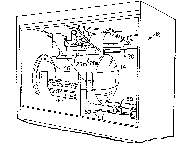
Referring to Figure l, there is shown a plasma barrel
reactor, generally designated 12. Reactor 12 includes a
generally barrel-like, cylindrical working chamber 14. Barrel
chamber 14 may have a diameter from six to 12 inches; the
diameter of chamber 14 is 12 inches in the pre-
Pgl - 4A -
~a~4~39
ferred embodiment. The axial length of chamber 14 is ap-
proximately 21 inches. Chamber 1~ has a plura]ity of entry
ports 16 for receiving a working gas and a plurality of ex-
haust ports 18 for venting various gases and by-products of
chamber 14. There are four entry ports 16 and five exhaust
ports 18 in the preferred embodiment. Moreover, entry
ports 16, as best illustrated in Figure 3, are positioned
diametrically opposite exhaust ports 18. Chamber 14, in
the preferred embodiment~ is made from a conventional inert
material such as quartz9
Chamber 14 is adapted to receive a plurality of arti-
cles 20. Articles 20, as shown, are semiconductor wafers
each of which has a layer of photoresist material on it
when the wafers are placed in chamber 14.
Reactor 12 further includes an entry gas manifold 22
that is positioned adjacent chamber 14. Entry gas manifold
22 is a tube, also made of ~uartz that has a plurality of
ports 24 each of which is in communication with one of the
barrel chamber entry ports 16. Entry gas manifold 22 in
the preferred embodiment has four ports 24. Entry gas
manifold 22 is capable of transporting the working gas to
barrel chamber 14.
A radio-frequency (RF) electrical energy generator,
not shown, is provided. In the preferred embodiment, the
frequency o the RF ener~y is 13.56 MHz.
In addition, reactor 12 includes a pair of entry port
electrodes 28e and 30e which are positioned adjacent barrel
chamber entry ports 16, as best shown in Figure 3. Each
of the electrodes 28e and 30e, which are manufactured from
a conductive metal such as copper, contains a slight curva-
ture in its design such that it follows the curvature of
chamber 14. Electrodes 28e and 30e are capable of creating
an electric field in barrel chamber 14 adjacent entry ports
16. This entry port electric field Ee then converts the
working ~as to a working plasma. Moreover, the position of
entry port electric field Ee delineates a substantially
.
39
--6--
electric field-free region FR in chamber 14 ad~acent arti
cles 20.
A pair of manifold electrodes 28rn and 3nm, which are
positioned adjacent entry gas manifold 22, is also pro-
vided. Each of the manifold electrodes 28m and 30m is agenerally vertically-extending plate that is positioned at
either side of manifold 22, as best shown in Figure 3.
Electrodes 28m and 30m are also manufactured from a conduc-
tive metal such as copper. Manifold electrodes 28m and 30m
are capable of creating an electric field in manifold 22.
~he manifold electric field Em converts a portion of the
working gas to the working plasma before the working gas
enters chamber 14. The combined effort of the manifold
electric field Em and the entry port electric field Ee
efficaciously convert the working gas to the desired work-
ing plasma.
Although electrodes 28e and 28m and electrodes 30e and
30m are claimed and described as separate and discrete
electrodes, electrodes 28e and 28m could be manufactured as
a single electrode and electrodes 30e and 30m as a single
electrode. In addition, manifold electrodes 28m and 30m
need not be required in all instances. Although the mani-
fold electric field Em generated by electrodes 28m and 30m
does contribute to the efficacious conversion of the work-
ing gas to the working plasma, its elimination does notdetract the overall conversion of the working gas to the
working plasma made by the entry port electric field Ee
alone.
Reactor 12 also includes a plasma flow constraint mem-
ber 40 that is positioned within barrel chamber 14. Con-
straint member 40 is a planar, board-like platform which
has a plurality of openings 42. Openings 42 perform two
functions the first of which is to receive wafers 20.
Wafers 20 are first placed into a conventional wafer recep-
tacle 44, which is generally referred to as a wafer boat.Each ~afer boat 44 is capable of receiving a plurality of
~ ~314~
--7--
wafers, as best shown in Figure 4~ The wafers in boat 44
are spaced apart sufficiently so as to permit the atomic
oxygen to flow among them and react with the photoresist
which are on the wafers. Boat 44, which is manufactured
from an inert material such as quartz, is then received in
opening 42.
The next, and more important, function of platform 40
is to restrict the flow of the working gas, and direct it
only to wafers 20. The working gas ceases to be a plasma
when it leaves the electric field. In prior art reactor
such as that shown in Figure 2, a substantially amount of
the working gas or in this instance, plasma, may never come
in contact with wafers 120. This is due to the fact there
is sufficient space in chamber 114 to permit the free drift
of plasma. In contrast, platform 40 is configured such
that it divides chamber 14 into two regions, a working
region 46 and an exhaust region 48. The only communication
between these two regions is through openings 42. This
design forces the working gas to pass only through openings
42, which are positioned immediately below wafers 20. This
causes all of the plasma to flow through wafers 20 and
react with the photoresist. Platform 42, which has
dimensions of approximately 21 inches X 9 inches X 1/8
inch, is manufactured from a non-reactive material such as
hard anodized aluminum. Platform 42 may also be
manufactured from quartz.
Reactor 12 further includes an exhaust manifold 50
that is positioned adjacent chamber 140 Exhaust manifold
50 is a tube, also made of quartz, that has a plurality of
ports 52 each of which is in communication with one of the
barrel chamber exhaust ports 18. Exhaust manifold 50 of
the preferred embodiment has five ports 52. Exhaust
manifold 50 is capable of transporting away from chamber 1~
any r0maining working plasma along with gaseous by-products
of the plasma-photoresist reaction.
:.
3~
In use, wafer boats 44 each of which that has a plu-
rality of wafers 20 are first placed in openings 42 of
platform 40. Chamber 14 is then evacuated to a moderate
vacuum, approximately 1/1000 of an atomosphere. The evac-
uation is accomplished by a conventional pump, not shown,that is connected to exhaust manifold 50. Diatomic oxygen,
the working gas, is admitted to chamber 14 via entry gas
manifold 22. ~ source of diatomic oxygen, not shown, is
connected to entry gas manifold 22~
The RF generator is then activated, causing electrodes
28e/ 28m, 30e and 30m to generate electric fields in both
entry gas manifold 22 and chamber 14. The electric fields
produced, Ee and Em, decompose diatomic oxygen to mono-
atomic oxygen, the working gasu The electric field in man-
ifold 22 converts a small portion of the working gas into
plasma before the gas enters ports 16 of chamber 14. The
remaining portion of the working gas is converted to plasma
by the electric field that is adjacent entry chamber ports
16. The position of the entry port electric field Ee
forces all of the working gas to pass through the field,
enhancing the conversion of gas to plasma.
As the working gas travels through chamber 14, its
route oE travel is dictated by constraint platform 40.
Instead of meandering around in chamber 14, which is the
case ~or plasma in prior art chambers, it can only exit by
passing through openings 42. Since wafers 20 are posi-
tioned irnmediately above openings 42, all of the plasma
must pass through wafers 20. Since this enhances the
number of oxygen-photoresist interactions, the time for
completing the entire photoresist removal process is re-
duced.
It will be apparent to those skilled in the art that
various modifications may be made within the spirit of the
invention and the scope of the appended claims.