Note: Descriptions are shown in the official language in which they were submitted.
t~3~t~L~7
This invention relates to a data transmission control
system which is able to perform a circuit switching -function in a
token rlng type local area network.
The present invention will be illustrated by way of the
accompanying drawings, in which:-
Fig. 1 is a block diagram of a node ln a token ring
network according to an embodirnent of the invention;
Fig. 2 is a flowchart showing the control function of a
controller useful in the network of Fig. l;
,,
Fig. 3 shows a data transmission sequence in the net-
work of Fig. 1;
Fig. 4 is a flowchart showing the control function of a
controller according to another embodiment of the invention;
Fig. 5 is a block diagram in more detail of the mode of
Fi~. l;
Fig. 6 is a block diagram of a basic clock generator
useful for the network of Fig. l;
Fig. 7 is a block diagram of a baslc clock generator
according to another embodiment of the invention;
Fig. 8 is a timing chart showing the generation of a
basic clock, the operation of a frequency divider in a basic
clock reproduction circuit and phase quant~zation;
Fig. 9 is a block diagram of the basic clock reproduc-
tion circuit of Fig. 8;
Fig. 10 is a block diagram of a basic clock generator
according to anoth r embodiment of the lnvention;
Fig. 11 is a table listing error data obtained from the
subtractor of Fig. 10;
Fig. 12 is a schematic diagram o~ -the varlable fre-
quency divlder shown in Fig. 10;
Fig. 13 is a timing chart showing the operation of the-
lo variable freqeuncy divider of Fig. 12 when a slave phase delya iscompensated for;
Fig. 14 is a timing chart showing the operation of the
variable fre~uency divider when a slave phase is leading the mas-
ter phase;
Fig. 15 shows the conditions to be met by a synchro-
nization unit according to the invention;
Fig. 16 shows a frame configuration according to the
invention;
Fig. 17 shows the operation of the synchronization unit
when the basic clock reproduction device of Fig. 9 is used;
Fig. 18 shows the operation of the synchronization unit
when the basic clock reproduction device of Fig. 10 is used;
Fig. 19 is a schematic diagram of a token ring network
according to the prior art; and
Fig. 20 shows the data transmission in the token ring
network of Fig. 19.
Heretofore, local area networks have been able to use
only a packet switching method and there are no local area net-
works making use of a circuit switching method. Since there isno prior art in this respect, a packet switching me-thod for a
token ring system will be outlined below.
Fig. 19 schematically shows a token ring ne-twork system
which includes terminals lOla through lOlc, termlnal ln-ter~ace
lines 102a through 102c, a unidirectional ring transmi,sslorl line
103, and nodes 104a through 104c each capable of reproduclng and
repeating s~gnals on the ring transmission line 103 and permit-
tin~ data transmission between the terminal 101 and the ring
transmission line 103. The data transmission to the termlnal 101
is effected via the terminal interfac2 line 102. A ring trans-
mission line controller 105 is provided for token control and
generation of a system clock to synchronize the entire system.
The central controller 105 may be replaced by a local controller
installed in each node 101.
~`
Fig. 20 shows the data transmission in the token ring
network of Fig. l9.~ A token arrives at the node 104a at a time
tO. At this time, the node 104a has data to be transmitted and
sends it out a~ a frame A to the ring transmisslon line 103 while
reproducing the token immediately after the frame A at a time tl.
The node 104b has no data to be transmitted and merely reproduces
and repeats the frame A and the token at the time t2. If the
frame A is addressed to the node 104b, the node 104b receives the
frame A while performing th~ reproduction and repeating~ At a
time t3, the node 103c transmits a frame C and reproduces the
token, while the frame A is reproduced and repeated by the
controller 105. At a time t4, the node 104a discards the frame A
which has completed a cycle of excursion through the ring
transmission line 103, and receives the token again. In this
Example, the token excursion time at ~he node 104a is ~t4 - to).
In this token ring network, the token excursion time is
the sum of the propagation time through the ring transmission
line 103 including the reproduction and repeating time at each
~ 7
node and the time length of a frame transmitted including the
time leng-th of a token. Consequently, it varies wldely depending
on the size of a system and the transmission status of each node.
secause of this variation, the token ring system networks, which
have been able to use a packst switching method, have been unable
to employ a circuit switching method.
In order to use a circuit switching method, it is nec-
essary to maintain a constant speed or rate o~ data transmission
between terminals. The variation in the token excurslon tlme,
however, presents the following problems. If the data transmis-
sion rate between terminals is x bits/sec (constant) and the
token excursion time is t sec (variable), then the transmitter ,
data buffer stores x~t bits of new data and transmits them to the
lS receiver data buffer via the r1ng transmission line 3. The data
received by the receiving buffer is transmitted to the receiving
terminal at the cons~ant rate of X bits/sec so that x t bits of
data are transmitted to the receiving terminal in t seconds.
Consequently, if the next data does not arrive at the receiving
buffer in t seconds, an underflow condition takes place in the
receiving buffer, resulting in a temporary interruption of data
transmission to the terminal. In the token ring system, the
token excursion ti~e always varies, and such an underflow
condition frequently occurs unless some countermeasure is taken.
otherwise~ it is impossible to implement a circuit switching
method in a token ring network.
Accordingly, the pres~nt invention provides a token
ring network system with a circuit switching function by elimi-
nating the data buffer underflow due to the token excursion vari-
ation in the token ring network.
According to one aspect of the invention there is pro-
vided a token ring network with a synchronlzation unit which
establishes synchronization between the particular nodes in the
network independently of both the synchronization of the network
-- 4
~ '2 ~7
as a whole and the communicatlon speed or rate of the nekwork.
The synchronization between the nodes is establlshed by mutually
transmitting clock phase data in packets.
According to another aspect of the invention, a prede-
termined amount of data is stored in a data buffer under the con-
trol of a controller, and data transmission from -the data buffer
is started a prede-termined period of tlme af-ter settlng-up o~ a
data transmisslon mode. Thus, no underflow condition takes placé
in the receiving data buffer.
Thus, according to the present invention there ls pro-
vided a data transmission control system for use in a node which ,~
connects a terminal to a ring transmission line in a packet mul-
tiplex network of a token ring system, said data transmissioncontrol systQm comprising a transmitter/receiver data buffer for
temporarily storing data transmitted to or from said ring trans-
mission line; basic clock generating means for generating a basic
clock and its phase data to be transmitted in a packet to a next
node to synchronize a basic clock of said next node; and a con-
troller for controlling data storage of said data buffer and tim-
ing of data transmission to said ring transmission line so as to
produce a (constant delay time which is twice a maximum token
excursion tim0 through said ring transmission llne) time delay
which is determined by information previously agreed upon in said
pa~ket multiplex network and with which sald transmitter~receiver
data buffer transmits data to said ring transmission line or said
terminal after it received said data. Suitably said time delay
is set twice as long as a maximum token excursion time through
said ring transmission line. Desirably said basic clock generat-
ing means comprises a basic clock generator and a basic clock
reproduction circuit.
In one embodiment of the present invention said basic
clock generator comprises an oscillator; and a frequency divider
for diving an oscillation frequency of said oscillator to provide
- 4a -
2~L47
a basic clock and digital values of individual ~requency division
stages to form phase data of said basic clock.
In another embodiment of the present invention said
basic clock generator comprises a frequency divider for dividing
a frequency of an externally supplied clock to generate a basic
clock to be applied to sald terminal while providing digital val~
ues of individual frequency division stages to form phase data of
said basic clock.
In a further embodiment of the present invention said
basic clock reproduction circuit comprises a master phase regis-
ter for holding digital phase data received from said ring trans-
mission line; a voltage co~trolled oscillator with its oscilla-
tion frequency controlled by an applied control voltage; a fre-
quency divider for dividing a frequency of said voltage con-
trolled oscillator to generate a slave clock to be applied to
said terminal while providing digital values of individual fre-
quency division stages to generate digital phase data of said
slave clock; a slave phase register for holding said digital
phase data received from said frequency divider, a subtractor for
subtracting an output of said slave phase register from an output
of said master phase register to provide a digital phase differ-
ence; and a digital-to-analog converter for converting said digi-
tal phase difference into an analog voltage to be applied to saidvoltage controlled oscillator as a control voltage.
In a still further embodiment of the present invention
said basic clock reproduction circuit comprises a variable fre-
quency divider with a variable clock division ratio; and meansfor controlling said variable clock division ratio by comparing
master phase receiv0d from said ring transmission line with slave
phase generated by said variable frequency divider so as to cause
said slave phase to follow said master phase.
The present invention also provides a token ring system
- 4b -
214~
packet multiplex network including a ring transmission line, and
first and second nodes connected to said ring transmisslon line
and functioning as a synchronization master and a synchronization
slave, respectively, when synchronization is established be-tween
said first and second nodes, said first node comprises a basic
clock generator for supplying a basic clock and its phase data
represented in a predetermined number of bits, said phase data
being sent out in a packet to said ring transmission llne, and
said second node comprises a basic clock reproductlon circuit
operable with said phase data received from said rlng transmis-
sion line so as to reproduce a clock synchronlzed with said basic
clock, said reproduced clock being used to establish synchroniza-
tion between said first and second nodes. suitably said first
and second nodes each comprises both said basic clock generator
and said basic clock reproduction circuit.
Prior to the description of embodiments of the
-~ o
- 4c -
L4
-5~
invention, a ~y~tem .for implementing a circuit 3witchin~
method in a token ring network by preventing the occurrence
of an underflow condition when ~ynchroniæation is present,
will be described, and then a synchronization unit ~or
lmplementinK -the 3Ynchronization will be de3cr:Lbed.
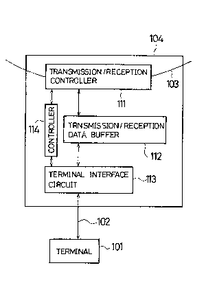
In FIG. 1 there is 3hown a ~ode 10~ which irlclude~
a ring tranamission/receptlon controller 111 provlded on a
rin~ transmis3ion line 103 for controlling tr~n~mission,
reception, repro~uction, and repeating of trarl3~1ssion data,
a transmission/reception d~ta bu~er 112 for temporarily
skoring transmi3slon data, a terminal interface circuit 113
for a terminal 101, and a general controller 114 for
controlling the respective devices 111 through 113. In this
embodiment, the terminal 101 ls an exclu~ive transmission
1~ terminal connected to the terminal interface 113 via a
terminal inter~ace line 102. The present invention concerns
a data transmisslon control system which is mounted ln the
seneral controller 114.
FIG. 2 shows an initial operation o~ the
controller 114 untll it is ready to start transmission of
data from the terminal 101 to the ring transmis~ion line 103
in response to a calling reque3t by the terminal 101 or a
calling reception from another node. As soon as a data
transmission mode is set up upon completion of a calllng
control mode in step~ 121 and 122, tran~mi~sion data ~rom
the termin~l 101 is fed to the data buffer 112. ~owever,
transmission of the data to the ring transmission line 103
in a s-tep 124 is enabled only when -the PassAge of a
predetermined period of time is found in a step 123.
If the predetermined period is tw and the
operational speed of the terminal interface is X ~its~sec.
then the amount of data sent out to the ring transmis3ion
line 103 is X~t~ bits. The data stored in the data buffer
112 is sent out to the ring tran3mission line 103 whenever a
token arrives. 'l`he amount of data stored in the data buffer
112 increases with the tlme. Thus, the decision of the
--6--
step 123 may be m~de bY ~lnding when the data stored ln the
data bu~fer 112 ha3 reached the prede-termined ~mount o~ data
or X-t~ bits. The stor~ge capacity of the data buf~cr 112
is m~de areater than X-tu bits.
The method of calculation o~ -the prede~ermlned
period of time tu will be de~cribed belo~r. F1~. 3 ~hows u
me-thod o~ data transmi3sion ~rom -the node ~ to the node ~.
Da-ta ~low~ into the node ~ from the terminal lOla at a rate
of X bits~sec and flows out from the node B to the terminal
101b at the same rate of X bits/sec. l'he ~orward
t~ansmission timc from the node A -to the node B is
represented by tFi (i = 1 2 3 ...) and the b~ckward
transmission time from the node B to the node A is
represented by t~j (j = 1 2 3 ...) wherein i and j are5 token excursion numbers on the ring -transmission line 103.
I~ the d~ata i3 transmitted to the rlng
transmission line 103 tu seconds a~ter lt ~lows out o the
terminal lOla X-tw bits o~ data are to be transmitted to
the node B. Upon reception of the da-ta the node B
transmits it to the terminal 101b a-t the rate of X bit~/sec.
Subsequently -the node A continues transmission to the ring
transmission line 103 while picking uP a token for each
excur~ion. The amount of data remained in -the receiver data
buffer immediately before the node B receives new data from5 the transmis3ion line 103 ln -the n--th excursion is
X-(tw - tsl - tF2 + tF1 ~ ts2 - tF 3 . . . - tu n -2 -
tFn-l + tFn-2 + tsn-2 - tU-I - tFn) bits.
When rearran~ed it becomes
X (tu + tFl - tFn-l - tsn-l - 'tFn ) bits.
I~ this value i5 negatlve there is an underflow conditior
in the d~ta bu~er. 'l'hls underflow condltion may be
eliminated by satisfying the followin~ condition
tu + tFl - tFn-l - tsn-l - t~n > 0 or
tu > ( tF n-l ~ tB n ~ ('tFn - tFI).
.35 The maximum values of (tFn-1 + tsn-l) and (t~n - -t~l) are
(tFmax + -t~max) and (tFmax - tFmin) respectivelY. 'I'he
21~
~7--
~ormer value corresponds to the ma~lmum token excursion tlme
while the latter Yalue to the maximum ~orward transmission
time between two nodes. HoweYer, there 1~ a cas~ where -the
next node is located in a direc-tion opposi-te to the
direction o~ data transmlssion. Hence, it will be seen that
eYen in the worst case, it is su~icien-t to set the
predetermined delay time -t~ to be a time perlod twlce RS
long as the maximum token excur~ion time.
Although the above de3crlPtion has been made on
the transmitter data buf~er, it is possible to apply it -to
the receiver data bu~er as shown in FIG. 4. The same
results may be obtained by provlding the predetermined delay
time tw ~or both transmitter and receiver da-ta bu~ers
according to the flow char-ts o~ FIGS. 2 and 4, respecti~elY.
A synchronization unit according to the invention
will now be described with re~erence to FIG. 5, wherein a
`node 104 is connected to a transmission line 103 via a
transce~ver 2. A..trarls!ni3sion/recep-tion controller 3
controls acces~ to the medium in the network system. and
transmission and reception o~ da-ta including ba~ic clock
phase data which will be described later. A transmitter
data buffer 4 temporarily stored transmission data ~rom the
terminal 101, which is connected to the node 104 via the
in-ter~ace line lOZ. The data stored in the da-ta bu~fer 4 is
sen-t out as a burst to the transmission line 103 when the
node 104 picks up a token for the right o~ transmission~ A
receiver data bu~fer 5 recei~es data ~rom -the transmiss:lon
line 103 and stores the data addressed to the terminal 101
and continuously sends out the stored data to the terminAl
101. 'l'he speed o~ communication on the transmission line
103 is made higher t~lan the communication speed o~ tlle
terminal l~l, and a continuous data stream on the terminal
interface line 102 is made to correspond to an intermitterlt
data stream in a time-compressed form on the transmission
line 103.
A ~asic clock generator ~ and a ~asic clock
4'-~
reproduction circuit 7 are u~ed to muke a 3ynchrorliza~ion
unlt accordinK to the invention. The basic clock generator
6 is used when the node 104 i~ a clock master, while the
baslc clock reproduction circuit 7 is used when the node 1~4
i~ a clock slave. ~ clock seleo-tor 3 3upplies ~he termlnal
101 wi-th either a master clock 14 o~ the ba3ia clcck
~enera-tor 6 or a slave clock 15 of the ~asic clock
reproduc-tion circuit 7 depending on a selector con~rol
~ignal 9 set bY the operator. It i8 possible to supply ~oth
the master and -the slave clocks 14 and 15 to the terminal
101 ~or respec-tive transmission and receiving ~unctions o~
the terminal 101. The clock selecting function, howevsr, is
irrelevant to the subject m~tter o~ this application and
will not be descrlbed ln detail. A terminal inter~ace
circuit 113 interface~ the transmitter and receiver data
buffers 4 and 5,~and -the clock selector 8 to the terminal
101. A termlnal inter~ace line 102 connecting the terminal
101 to the interface circuit 113 may be a stand~rd inter~ace
such as RS232C.
FIG. 6 showa the basic cloak generator 6 according
to an embodiment o~ the inven-tion. A ~reguency divider 62
divides a ~requency of osclllation generated by an
oscillator 61 to produce intermediate frequencies. l'his
~requency dlvider 62 is a one-eighth frequency divider. Its
25 -last stage outputs a master clock 14 which is supplied to
the terminal 101. Four b1t data on the individual frequency
dl~ision stages ~/B, q~4, ~2, and ~ is supplied as phase
data of the n~aster clock 14 to the transmission~recePtion
controller 3. That ls, the frequency divider 62 generates
both the master clock 14 and its digital phase data in a
single circult.
FIG. 7 shows the basic clock generator 6 in more
detail, wherein a ma~ter-side master phase register 63 holds
digital phase data from the frequencY divider 62. The
frequency divider 62 is a one~eighth frequency divider. Its
last stage outputs a ma~ter clock 14 which is supplied to
_9_
the terminal 101, while its respective frequencY divi~on
stages 3upply digltal phase dat~ ~a, 1~4, ~2, and f~ of
the master c:lock 14 t,o the master phase register 63.
Whenever a Phase data packet is transmi-tted to -the
network~ the content~ of the master phase re~lster 63 are
updated in re3pon3e to a pha3~ data -tr~n~ml~ion ~tart Pul~e
32 ~rom tlle transmi3sion/receptiorl oon-troller 3. 'l'he
upd~ted contents of the master pha~e regis-ter 63 (the
digit~l phase da-ta of the master clock 1~ when -I;he pRC~Ce t
transmission is started) are tr~nslllitted to the network as
the content3 of -the packet~ The frequencY divider 62
generate~ both the ma~ter clocX 14 and its digital phase
data in A single circuit.
FIG. a 3hows the input and outputs of the
fre~uencY divider 6Z indica~ing that the Phase o~ a cycle
(2 O o~ the ma~te~r clock 14 is digitali~ed in ~8 steps (4
bits). ~s phase data of the Master clock 14, the mas-ter
node transmits the newest digital phase data; n~melY, the
digikal phase data at the time of start of -transmission.
FIG. 9 5]lOwS the basic clock reproduction circuit
7 which includes a 4-bi-t master phase register 71 for
holding the digital phase data transmltted from the maste.r
node via the transmission/reception controller 3 and a slave
phase register 72 for holding the digital Phase data of the .
slaYe clock 15. The contents of the re~isters 71 and 7Z are
updated in response to A phase data recepSion pulse 31 which
is supplled by the transmi~sion/reception controller 3 upon
reception of the master phase data. A subtractor 73
provides a Phase difference between the contents o~ the
registers 71 and 72. The dlgital phase di~ference is
converted into an analog voltage in a digital-to-analog
converter 74. The analog voltage is applied to a voltage-
controlled oscillator (VC0~ 75 to control the fr~quency of
the oscillator 75. The ou-tput of the VCO 75 .is applied to a
frequency divider 76 which is similar to that of FIG. 7.
The fre~uencY divider '76 ~enerates a slave clock 16 which is
applied to the terminal 101 and digital phase d~ta o~ -the
slave clock 15 which ls applied to the slave phas~ register
72. The basic clock reproduction circuit 7 is basically -the
3atne ~5 the prior art PLL (phase~locked loop) excep-t that
the phase data i3 sampled and compared so that the slave
phase may be locked to the mast~r phAse b~s~d on -tlle
sampling -theory as ~ar a3 varlations in the phasc
dlfference are within the limits for the samplin period.
FIG. 10 shows the basic clock repro~uction circuit
7 according -to arlother e~bodiment o~ the invention. A
variable ~requency divider 76A divides the frequencY of a
reproduction clock a-t a predetermined ratio to proYide the '
slave clock 15 and its slaYe phase data. A subtractor 73A
subtracts the slave phase data ~rom the master phase data
transmitted ~rom ~he master node via the transmission/
reception con-trol~er 3 to provide a difference between the
master and sla~e phase data and applied to the ~requencr
divider 76~ part~or all of the error data as phase control
data 7lA.
Whenever the master phase data is received, a
phase clata reception pulse 31 is apPlied to the variable
frequency dlvider 76A to hold the value of the phase control
data 71A at the time. The variable frequency dlvider 76A
adiusts the slave phase according to the held value to keep
constant the error between the master and slave phases.
More specifically, if the slave phase is lagging behind the
master phase, the phase control data 'llA has a positiYe
value. In this case, the variable frequency divider 7~A
reduces the frequency divi~ion ratio to advance the slave
phase. I~ the ~lave phase is leading the master phase, the
phase control da-ta 71A is negative. Thus. the variable
1'requency divider 76~ increases the ~requency division ratio
to slow the slave phase.
FIG. 11 lists errors in the 4-bit phase da-ta
expressed in hexadecimal numbers. It will be seen from the
table -that the 31ave phase is in step wit]l or luggin~ behin(3
4~
-11-
the ma3ter phaqe when the error data is between 0 and 7
(l.e., positive) and ahead of the master pha~e when the
error dat~ i3 be-tween 8 and F (i,e., negative). Hence, i-t
is possible to control the variable frequency divider 7
with the use of only the si~n blt (i.e., 1~ pha~e clata) o~
the error data. In the embodlment o~ FI~. lO, the phase7
of the error data is used a~ the phase control ~a-ta 71~.
Fl~. 12 shows the variable frequency divider 76h,
the configuration whereof is well known. ~f -the output of
an AN~ gate G2 is "H" at all timeq, a J-K flip-~loP FF3
merely divides the frequency of the reproduction clock 63
into one half and cons-titutes a 1/512 frequency divider with
synchronous 4-bit counters C1 and C2 on the subsequent
~tage.
FIG. 13 shows the operation of -the variable
~re~uency divider~76A when ~ delaY of the slave phase is
compen3ated for. When the slave phase is lagging behind the
master phase, the phà~e control data 71A is "L" and a flip-
flop FFla is set with the trailing end of a phase data
reception pulse 31. When the output Q of -the ~liP-floP FFla
goes to "H" and the output Q of a ~lip-flop FF3 hecomes "L",
the output of an ANV gate Gla becomes "H". When a pulse of
the reproduction clock 63 is generated under this conditioll.
the output Q of the ~lip-flop FF3 becomes "H" with the
trailing end of the clock pulse. At the same time, the
output Q of the flip-flop FF2a goes to "H" and the ~ lop
FFla is reset. When the flip-flop FF2a is set~ the output
of an AND gate G2 becomes "L". Consequently, the flip-~lop
FF3 remalns in the same state to hold Q ~ "H" when the next
3~ clock puls0 is generated. Thus, a carrY inpu-t (CI) is
applied to the next stage sYnchronous 4-bit counter C1 for
two successive clock pulses to effect phase advancement by
~512.
When the Yariable fraquencY divislon control is
not provided, the operation of the flip-flop FF3 and the
outpu-t of the counter C1 in termq o~ ~/128 are ~hown bY
~'Z ~7
~12-
da~hsd lines.
FI~. 14 shows the opera-tion of -the variable
~re~uency divider 76~ when -the slave phase ls ahead of -the
master phase. This operation i3 easy to understand from the
above descri~-tion and will not be descrlbed in de~,all.
Through -the above varlable ~requency divlsion oorItrol, the
slave phMse ls controlled so as -to follow t~e master phas~
which is transmitted via the paclce-t mul-~iplex network. 'I'he
number of frequencY dlvlsion stages ln the v~riable
frequency divider 76A and the bit width Or the master an-l
sl~ve phase data are determined from the difference between
the transmlssion and reception clocks, the master phase
transmission intervals, and the allowable error between t~le
master and sla~e phases.
The synchronization system according -to the
invention will now be described with reference to FIGS. 15
through 18. In FIG. 15, with this synchroniza-tion system,
the present time tn'may be measured under the con-trol of the
transmitter or mas-ter clock and transmitted as phase data to
the receiver to correc~ a leading or laggin~ error ~an of
the receiver or slave clock t~n, whereby the slave clock is
3ynchronized to the master clock. In this case, the
transmisslon delay or time f must be cons~ant whereas the
transmlssion intarvals tn~l - tn need not be constant. The
maximwn transmission interval ls determined bY the extent of
an error bet-.ween the transn~ sion and reception clocks.
As is apparent from the frame configllratioIl shown
in FIG. 16, when the ~rame category E`C is a time frame. the
data INF~ represents the Phase data of a master cloclc. ln
3~ this embodiment, the phase data has a fixed 4-bit length so
that the :Lrame constltutes a packet of a Eixed lenfr-tII.
Hence, tIIe ~ransmission time ~ is constant. In addition. in
a packet multiplex network such as a token ring or bus
ne-tworlc. the upper limit of a transmission waiting tiIl)e at
each node is determined by the excurslon time of a -token.
'rhis condition may be me-t by making the components of ~he
4~
. ,
--13--
ba3ic clock generator 6 and the clock reproduction circuit 7
sufflclently precise to allow A certain error b~tween the
-tran~mission and receptlon clocks even when the
transn~i3sion waiting time is at the maxinlum lovel. ln th;Ls
way, -the slave clocl~ is synchronized to l~he m~ l;or clools OJI
the receiving end by receiving the transllli-tter preselllt l;lme
data to correct -the slave clock 50 that, l;he error a,. o.r
'n~ n i~ constant.
The operation of the synchronlzation ~ystem will
now be described in detail with re:Eerence to FIG. 17. The
oscillation Irequency of an os~illator 61 is divided by a
frequency divider 62 in the transmitter to produce a master
clock having a f requency of :eO Hz and a Phase ~o obtainPd
by quantization in7~8 steps. The phase da-ta ~10 at a time
tl is sampled and tr~nsmitted to~ the network as t~le time
data ti OlC a :~rame'` such as shown in FIG. 16. This phase
data ~o(ti ) reaches the receiving end a~ter the network
tran31ni~;ion ti me ~7~ ancl i~3 sub~ec ted to parallel--l;o-serial
conversion in a receiving register 3a in the transmission/
reception controller 3. At this point, a phase data
reception pulse 31 is generated by the transmission~
reception controller 3 based on the :~rame category FC of the
received frame. Consequently, the phase data ~o (ti ) is
held in a master regis-ter 71 while the phase da-ta 6~c ( ti ~ r~
' 25 of a fc -H~ ~lave clock at A time ( tl + ~) ls sampled and
held in a slave phase re~ister 72. The respective phase
data ~o (tl ) and ~9c (ti ~ ~) in the registers 71 and 72,
respectively, are then applied to a subtractor 73, which
consists of a complement circuit 73a and an adder 73b, to
provlde a phase dlfference between these two pieces o~ data.
This di~ital phase di~ference is converted lnto analog data
in a D/A converter 74. This analog data proportional to the
phase difference ~o (ti ) - ~c (ti ~ ~ ) is applied to a
voltage- controlled oscillator 75 as a control voltage. The
os~illation frequency o:l~ the VC0 75 is controlled so as to
keep I;he phase difIerence constant, and the output of the
VC0 75 ls applled to a ~requencY divider 76. The frequency
divider 76 divides the oscillation frequency to genera-te a
slave clock synchronized to the master clock and its phase
data ~c for ti~in~ the reception o~ the next phase data
reception pul~e 31.
Accordln~ to the sampling theory, -the condltion3
required for the above synchronlæation are th~t the network
transmi3sion time ~ is constAn-t and that the mlnlmum
sampling frequency l/(tn+l - tn )max~ wherein (-tn~l - tn) ls
1~ the tran~m1s3ion interval, is at lea~t twice as large as the
maxlmum di~erence betwcen the master clock ~requency fo
and the sl~ve clock frequency f~. Since the transmis3ion
time ~ ls cons-tant as described above. bY making the phase
difference variation amall for -the samp1irlg cycle period,
the slave phase may be locked to the master phase. Hence,
it is possible to e~tablish synchronization between two
geographically remote nodes in the network bY transmitting
the master Ph~se ~at~ through the network.
FIG. 18 shows the synchronization system employlng
the circuit o~ FIG. 10 as a basic clock generation device.
~'he phase data ~o of a fr~me reaches the receiving end a~ter
the network transmission tlme T and undergoes serial--to-
parallel conversion in the receiving register 3a in the
transmission/reception controller 3. At this point~ a phase
data reception pulse 31 is genera-ted by the l`/l~ con~roller 3
- based on the frame category FC of the received frame. The
phase control data 71A ob-tained ~rom a subtractor 73A is
applied to a variable frequency divider 76A for variable
frequency di.vision control as described above. 'l'hus, Lhe
3~ slave p~lase is synchronized to the master phase.
lf clock synchronization between a number of nodes
is established, a circuit switching method may be used in a
packet multiplex network. According to the invention, the
address data DA of a frame such as shown in l~r~. 11 may be
used -to implemen-t ttle following three different
synchronization systems.
.
-15-
~ (1) When the D~ is used as broadcast ~ddress dQtR,
the entire ~ystem m~y be synchronlzed to a sinKle master
~lock.
(2) When the DA i.~ used ~s multicast addre3s dat~,
synchronization maY be establi3hed in each ~roup havin~
master clock.
(3) When the ~ i3 used a~ in~lvi~ual Addreas
data, synch.ronization may be establlshed fox each Pair o~
mating nodes.
In other words, it is po~slble to provide a token
ring network with a circuit switchin~ ~unctLon at a given
communication speed or rate without using any particular
controller for controlling the en-tire network (case 1).
Also, it i5 possible to form A network wherein different
s~nchronization systems are present, which has been
imposs~ble beforep(cases 2 and 3). In these ca~es, circuit
swltching at a given communicatlon rate may be imPlemented
between the mating nodes independently of both the
3ynchronlzation of the network a~ R whole ~nd the
communicatlon rate of the network.
Although the oscillator 61 i5 pro~ided in the
ba~ic clock ~enerator 6 in the ~bove embodiments, it i3
possible to use a clock supplied from the outside as an
output of the o~cillator 61 for es-t~bllshing synchronizatlon
between nodes under the control o~ the external clock. In
addition, the node 104 include~ both the basic clock
generator 6 ~nd the clock reproduction circult 7, but it is
possible to use only one of them depending UPon the node.
With the synchronization system according to the
invention, it is possible to establish ~ynchronization for
implementing a circuit switching method in a packet
multiplex network, such as a token rin~ or bus ne-twork.
independently of both the synchronization of the network as
a whole and the communication rate of the network.