Language selection

Search

Patent 1282467 Summary

Third-party information liability

Some of the information on this Web page has been provided by external sources. The Government of Canada is not responsible for the accuracy, reliability or currency of the information supplied by external sources. Users wishing to rely upon this information should consult directly with the source of the information. Content provided by external sources is not subject to official languages, privacy and accessibility requirements.

Claims and Abstract availability

Any discrepancies in the text and image of the Claims and Abstract are due to differing posting times. Text of the Claims and Abstract are posted:

  • At the time the application is open to public inspection;
  • At the time of issue of the patent (grant).
(12) Patent: (11) CA 1282467
(21) Application Number: 1282467
(54) English Title: METHOD FOR PACKAGING A MICROWAVE TUBE MODULATOR
(54) French Title: METHODE DE CONSTRUCTION DE MODULATEUR DE TUBE MICRO-ONDES
Status: Term Expired - Post Grant
Bibliographic Data
(51) International Patent Classification (IPC):
  • H01L 25/16 (2006.01)
  • H01L 23/66 (2006.01)
  • H01L 25/11 (2006.01)
(72) Inventors :
  • EHRENHALT, DAN (United States of America)
  • GILES, GEORGE RODNEY (United States of America)
(73) Owners :
  • DRS C3 SYSTEMS, INC.
(71) Applicants :
  • DRS C3 SYSTEMS, INC. (United States of America)
(74) Agent: SMART & BIGGAR LP
(74) Associate agent:
(45) Issued: 1991-04-02
(22) Filed Date: 1988-11-07
Availability of licence: N/A
Dedicated to the Public: N/A
(25) Language of filing: English

Patent Cooperation Treaty (PCT): No

(30) Application Priority Data:
Application No. Country/Territory Date
156,175 (United States of America) 1988-02-17

Abstracts

English Abstract


P-324
METHOD FOR PACKAGING A
MICROWAVE TUBE MODULATOR
ABSTRACT
A method for packaging components in the primary
circuit of a microwave tube modulator output transformer.
Modules are assembled using parallel plates upon and
around which transistors and other necessary components
are mounted. In addition to providing mechanical support
for the components, the plates act as conductors for
circuits common to respective elements of paralleled
transistors, thereby minimizing electrical resistance and
inductance in the primary circuit. The modules are
designed to mount to the output transformer such that two
of the parallel plates are mechanically connected to the
respective two ends of the transformer primary, and a
number of modules can be mounted around and to one
transformer according to the amount of energy required.


Claims

Note: Claims are shown in the official language in which they were submitted.


P-324 -8-
WHAT IS CLAIMED IS:
1. A method for packaging into an effective
module components, particularly power transistors, in the
primary circuit of a microwave tube modulator output
transformer to minimize electrical resistance and
inductance in the primary circuit, the process comprising
the steps of:
connecting a first plate to a first end of the
microwave tube modulator output transformer primary, and
connecting said first plate to a source of positive
voltage;
mounting a second plate in spaced apposition to
said first plate, and connecting said second plate to
ground;
mounting a third plate in progressively spaced
apposition to said first plate and said second plate, and
connecting said third plate to a second end of the output
transformer primary; and
mounting a plurality of primary circuit power
transistors on said third plate at minimum practical
distances from the second end of the output transformer
primary such that the common element of each of said power
transistors is connected to said third plate and therefore
effectively connected to the second end of the output
transformer primary, said first plate providing a low
resistance path for current flowing between the output
transformer primary and the source of positive voltage and
said third plate providing a low-resistance path for
current flowing between the respective drain elements of
said power transistors and the output transformer primary,
said first and said third plates also minimizing
inductance in the output transformer primary circuit.

P-324 -9-
2. A method according to Claim 1 further
comprising the step of connecting said power transistors
in parallel.
3. A method according to Claim 2 wherein said
power transistors are field-effect transistors.
4. A method according to Claim 3 further
comprising the step of connecting said power transistors
in a common gate configuration to minimize the effects of
drain-to-gate capacitance and thereby increase the
switching speed of said transistors, the gate element of
each of said power transistors being connected to said
third plate and therefore effectively connected to the
second end of the output transformer primary.
5. A method according to Claim 1 further
comprising the step of mounting to said second plate a
coupling transformer having a primary, a feedback and a
secondary winding, said feedback winding having a common
end and an output end, the common end being connected to
ground, said secondary winding having a common end and an
output end, the common end being connected to ground.
6. A method according to Claim 5 wherein said
coupling transformer is mounted central to said second
plate and between said second plate and said third plate.
7. A method according to Claim 1 further
comprising the step of mounting a fourth plate in spaced
apposition to and electrically isolated from said third
plate, and connecting said fourth plate through respective
fuse resistors to the source element of each of said power
transistors.

P-324 -10-
8. A method according to Claim 7 further
comprising the step of connecting said fourth plate to
the output end of the secondary winding of said coupling
transformer.
9. A method according to Claim 8 further
comprising the step of mounting a fifth plate in spaced
apposition to said third plate and electrically isolated
from said third plate and said fourth plate, and
connecting said fifth plate through respective parasitic
limiting resistors to the gate elements of said power
transistors.
10. A method according to Claim 9 further
comprising the step of connecting said fifth plate to
ground.
11. A method according to Claim 1 further
comprising the step of connecting a plurality of
capacitors between said first plate and said second plate
such that the connections provide both electrical
continuity and mechanical support for said capacitors.
12. A method according to Claim 1 further
comprising the step of mounting a plurality of driver
transistors to said second plate.
13. A method according to Claim 12 wherein said
driver transistors are connected in parallel.
14. A method according to Claim 13 wherein said
driver transistors are field-effect transistors.

P-324 -11-
15. A method according to Claim 14 further
comprising the step of connecting said driver transistors
in a common source configuration, the source element of
each of said power transistors being connected through a
respective fuse resistor to said second plate and
therefore effectively connected to ground.
16. A method according to Claim 15 further
comprising the step of connecting the drain elements of
said driver transistor to a first end of the primary
winding of said coupling transformer.
17. A method according to Claim 16 further
comprising the step of connecting the second end of the
primary winding of said coupling transformer to the source
of positive voltage.
18. A method according to Claim 17 further
comprising the step of connecting the output end of the
feedback winding of said coupling transformer through
respective resistors to the gate elements of said driver
transistors, said gate elements being connected through
other respective resistors to an input signal source.
19. A method according to Claim 1 further
comprising the step of connecting a plurality of modules
to a single microwave tube modulator output transformer
to increase the electrical energy available for the
operation thereof.
20. A microwave tube modulator having an
effective disposition of components, particularly power
transistors, in the primary circuit of a microwave tube
modulator output transformer to minimize electrical

P-324 -12-
resistance and inductance in the primary circuit, the
modulator comprising:
a first plate connected to a first end of the
microwave tube modulator output transformer primary and
to a source of positive voltage;
a second plate disposed in spaced apposition to
said first plate and connected to ground;
a third plate disposed in progressively spaced
apposition to said first plate and said second plate, said
third plate being connected to a second end of the output
transformer primary; and
a plurality of primary circuit power transistors
mounted on said third plate at minimum practical distances
from the second end of the output transformer primary such
that the common element of each of said power transistors
is connected to said third plate and therefore effectively
connected to the second end of the output transformer
primary, said first plate providing a low-resistance path
for current flowing between the output transformer primary
and the source of positive voltage and said third plate
providing a low-resistance path for current flowing
between the respective drain elements of said power
transistors and the output transformer primary, said first
and said third plates also minimizing inductance in the
output transformer primary circuit.
21. A modulator according to Claim 20 wherein
said power transistors are connected in parallel.
22. A modulator according to Claim 21 wherein
said power transistors are field-effect transistors.
23. A modulator according to Claim 22 wherein
said power transistors are connected in a common gate

P-324 -13-
configuration to minimize the effects of drain-to-gate
capacitance and thereby increase the switching speed of
said transistors, the gate element of each of said power
transistors being connected to said third plate and
therefore effectively connected to the second end of the
output transformer primary.
24. A modulator according to Claim 20 further
comprising a coupling transformer mounted to said second
plate, said coupling transformer having a primary, a
feedback and a secondary winding, said feedback winding
having a common end and an output end, the common end
being connected to ground, said secondary winding having
a common end and an output end, the common end being
connected to ground.
25. A modulator according to Claim 24 wherein
said coupling transformer is mounted central to said
second plate and between said second plate and said third
plate.
26. A modulator according to Claim 20 further
comprising a fourth plate disposed in spaced apposition
to and electrically isolated from said third plate, said
fourth plate being connected through respective fuse
resistors to the source element of each of said power
transistors.
27. A modulator according to Claim 26 wherein
said fourth plate is connected to the output end of the
secondary winding of said coupling transformer.
28. A modulator according to Claim 27 further
comprising a fifth plate disposed in spaced apposition to

P-324 -14-
said third plate and electrically isolated from said third
plate and said fourth plate, said fifth plate being
connected through respective parasitic limiting resistors
to the gate elements of said power transistors.
29. A modulator according to Claim 28 wherein
said fifth plate is connected to ground.
30. A modulator according to Claim 20 further
comprising a plurality of capacitors connected between
said fir t plate and said second plate such that the
connections provide both electrical continuity and
mechanical support for said capacitors.
31. A modulator according to Claim 20 further
comprising a plurality of driver transistors mounted to
said second plate.
32. A modulator according to Claim 31 wherein
said driver transistors are connected in parallel.
33. A modulator according to Claim 32 wherein
said driver transistors are field-effect transistors.
34. A modulator according to Claim 33 wherein
said driver transistors are connected in a common source
configuration, the source element of each of said power
transistors being connected through a respective fuse
resistor to said second plate and therefore effectively
connected to ground.
35. A modulator according to Claim 34 wherein
the drain elements of said driver transistors are
connected to a first end of the primary winding of said

P-324 -15-
coupling transformer.
36. A modulator according to Claim 35 wherein
the second end of the primary winding of said coupling
transformer is connected to the source of positive
voltage.
37. A modulator according to Claim 36 wherein
the output end of the feedback winding of said coupling
transformer is connected through respective resistors to
the gate elements of said driver transistors, said gate
elements being connected through other respective
resistor to an input signal source.
38. A modulator according to Claim 20 wherein
a plurality of modules are connected to a single microwave
tube modulator output transformer to increase the
electrical energy available for the operation thereof.

Description

Note: Descriptions are shown in the official language in which they were submitted.


- ~82467
P-324 1-
NETNOD ~OR PACKAGING A
MIC~O~E TUB~ ~ODULA~OR
~ECHNICAL BACRGROUND
This invention relates to the packaging of
modulators used to provide high-voltage pulses to
microwave transmitter tube output transformers.
BACKGROUND AR~
A number of devices have been designed to
~ provide ~ulse~ for use in microwa~e modulation
; 15 applications. Some o~ these use field-e~fect transistors
~FET's) c~nec~ed in parallel to provide the necessary
energy to drive a microwave tube modulator output
transformer, but such configurations do not minimize
electrical resistance and inductance in the primary
20 circuits of the associated output transformers and require
modifications to increment their energy-providing
capacities. See, for example, U.S. Patent Numbers
3,374,406; 3,374,407; 3,426,255; 3,509/567r 3,525,861;
3,544,399; 3,56~,672; 3,582,975; 3,828,324; 3,gl4,555;
Z5 3,9~7,217, 3,9~5,178; 4,010,450; 4,071,777; 4,095,251;
~,143,387, 4,221,0~4, 4,235,010 4,247,903; 4,262,296;
4,304,042; 4,328,470; ~,409,594: 4,4~5,527: 4,662,~58;
4,679,050, 4,679,299: 4,683,387; and 4,689,~02.
The present invention provides a modulator
30 comprising elements in a combination and configuration
that simultaneously minimizes the electrical resistance
and inductance in the primary circuit of i~s associated
microwave tube modulator output transformer and
facilitates the combining of modulator units to supply
: 35 incrementally increased amounts of energy to the output
q~

X~3~4~7
P-324 -2-
transformer.
DI~CLOSURB OF T~2 INVENTION
In accordance with the present invention, a
modulator is provided that is capable of supplying high-
voltage pulses having short rise and fall times to the
primary windings of appropriately selected transformers
connected to a large number of different microwave
- transmitter tubes such as magnetrons, pulse cavity
oscillators, cross field amplifiers and traveling wave
tubes.
The preferred embodiment of the present
invention contemplates a modulator having a plurality of
plates used to mount components such as ~ransistors and
transformers such that the critical distances between the
components ar~ minimizsd, thereby contributing to the
minimization of electrical resistance and inductance in
associated circuitry.
The invention further contemplates a modulator
having a plurality of plates used to mount components such
that the plates ac~ as electrical conductors between
common elements of the components to additionally
contributa to the minimization of electrical resistance
and inductance in associated circuitry
The invention also contemplates a modulator
having a configuration enabling it to be combined with
like modulators to provide incrementally greater amounts
of energy.
The invention additionally contemplates
modulator that can, by combining an appropriate n~mber of
modulator units and using appropriate output transformers,
be matched to a large number of microwave transmitter
tubes.

?3Z467
P-324 3-
The invention further contemplates a modulator
that is relatively small.
The invention also contemplates a modulator that
is relatively easy to produce and maintain.
BRIEF DE~3CRIP~ION OF THE: DR~IING~
: `~
~n the drawings~ in which like reference
characters indicate corresponding parts in all the
lo figures:
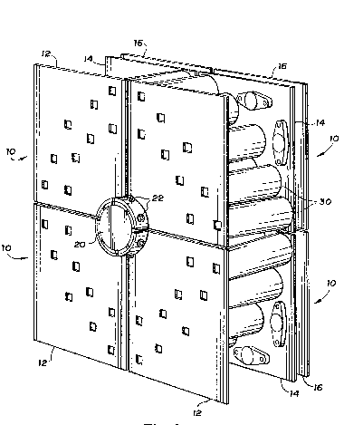
FIG. 1 is a perspective view of four microwave
tube modulator units connected to a microwave tube output
transformer and e~bodying features of the invention,
FIG. 2 is a perspecti~e view showing the
oppo~ite side of one of the units of FIG. 1
FIG. 3 is a side view, partly broken away, taken
alang the line 3-3 o~ FIG. ~ and
~IG. 4 is a rear view of one of the plates of
- the modulator.
D13T~II.ED DE8CRIP~ION
OF THIS PR~1~;3RRED B2ZBODIME~l' OF T~113 I~NVE:Nq~ION
Essentially, the microwave tube modulator is
assembled on and between three main plates and two smaller
plates. The plates serve as mounts for the components and
also as low-re~istance electrical c~nductors between
common elements thereof. The plates and components are
arranged to minimize the distances between the components
in the primary circuit of an associated output
transformer, thereby minimizing electrical resistance and
inductance, and also to facilitate the combining of a
~umber of modulator units to provide incrementally
increased energy to drive one output transformer.
With reference to FIG. 1, shown is a perspective
~ .

24~
P-324 -~-
view of four microwave tube modulator units~ generally
indicated by reference characters lo. Each modulator unit
10 has a first plate 12, a second plate 14 in spaced
apposition thereto, and a third plate 16 in progressively
spaced apposition to the first plate 1~ and the second
plate 14. The plates 12, 14, and 16 are electrically
isolated from each other.
FIG. 2 is a perspective view from the opposite
direction of one of the modulator units 10, and FIG. 3 is
lo a side view taken along the line 3-3 of FIG. 2. An
associated output transformer 18 is shown in FIG. 3. The
first plate l2 is secured to the first end 20 of the
primary of the transformer 18 with screws 22, and the
third plate ~ is secured to the second end 24 of the
primary of the transformer 18 with screws ~6. The second
plate 14 is secured to the third plate 16 by posts 28 but
is electrically isolated from the second plate 14 and the
second end 2~ of the kransformer primary. Connected to
and extending between the first plate ~2 and the second
plate 4 are a number of primary ~urrent storage
capacitors 30. The first and second plates 1~ and 14
serve as mounts for the capacitors 30 and also as low-
resistance electrical conductors therefor, the first plate
12 being connected to a source of positive voltage and the
second plate 1~ being connected to ground.
Mounted on the third plate 16 are a plurality
of power transistors 32, which may be field-effect-
transistors (FET's). The transistors 32 are connected in
parallel, and the drain element of each is connected to
the third plate 16. The transistors 32 are connected in
a common gate configuration to minimize the effects of
drain-to-gate capacitance and th~reby increase the
transistor switching speed. The plate 16 serves both as
a mount for the transistors 32 and as a low-resistance

~ ~32467
P-324 -5-
electrical conductor between the drain elements of the
transistors 32 and the second end 2~ of the primary of
the output transformer 18. As can be seen in FIG. 2, the
transistors 32 are arranged in close mutual proximity to
minimize the distances between connections to their
respective elements.
Mounted to the second plate 14 are a plurality
of driver transistors 42, which may be field-e~fect-
transistors. The driver transistors 42 are connected in
parallel, and the source element of each is connected
through fuse resistors (not shown) to the second plate
14. The plate l~ serves both as a mount for the
transistors ~2 and as a low-resistance electrical
conductor between the source element fuse resistors and
ground. The drain elements of the driver transistors 42
are connected to a first end of the primary winding of a
coupling transformer 3B mounted centrally to the second
plate 14. The second end of ~he primary winding of the
coupling transformer 38 is connected to a source of
po~itive voltage. The gate elements of the driver
transist~rs 42 are connected through resistors to a first
end of a feedback winding of the coupling transformer 38,
and the second end of the feedback winding is connected
to ground. The driver transistors 42 and associated
resistors form a dri~er circuit that amplifies incoming
signals before they are introduced to the primary circuit
of the output transformer 18 through the coupling
transformer 38.
FIG. ~ is a view of the surface of the third
plate 16 that faces the second plate 14. As shown in
FIG's. 3 and 4, a fourth plate 34 is mounted proximate
the third plate ~6 but is electrically isolated and
separated therefrom by an insulator 36. The fourth plate
34 is connected through fuse resistors (shown only

3246~
P-32~ -6-
representatively in FI~. 3) to the source element of each
transistor 32 and serves as a low-resistance conductor
between the source fuse resistors and one end of the
output winding of a trans~ormer 38 coupling a driver
amplifier to the primary circuit of the modulator lo.
A fifth plate 40 is mounted proximate the third
plate 16 but is also electrically isolated and separated
therefrom by insulator 3~. The fifth plate ~0 is
connected through parasitic-oscillation-limiting resistors
(shown only representatively in FIG. 3) to the gate
element of each transistor 32 and ~erves as a low
resistance conductor between the gate resistors and
ground.
In the embodiment of the in~ention shown in
~IG's. 1 and 3, up to four modulator units 10 may be
secured to one output transformer 18 to provide four
incremental levels of electrical energy. The first plate
12 of each modulator 10 may be secured to the first end
20 of the primary of the transformer 18, using screws 22,
and the third plate 16 of each modulator ~0 may be secured
to th~ second end 2~ of the primary of the transformer 18,
using screws ~6. Such a configuration brings the
components in the primary circuit of the transformer 18
into close proximity with each other and with the
contacting ends 20 and 24 of the primary of the output
transformer 18, thus keeping the current paths short and
the attending resistance and inductance at a minimum.
It should be understood that, depending on the
application and other engineering considerations and
requirements, the specific assignment and disposition of
the plates and certain other components may vary. For
example, to reduce the possibility o~ injury from electric
shock in applications where there is a likelihood that
personnel may have to work in the proximity of an exposed

467
P-324 -7
modulator assembly, the plates may be arranged so that the
innermost plate i5 the one connected to a voltage source
and the outermost plate is grounded. Similar changes and
modifications may be made to accommodate requirements of
cooling, space, and the like without departing from the
spirit and scope of the invention.

Representative Drawing
A single figure which represents the drawing illustrating the invention.
Administrative Status

2024-08-01:As part of the Next Generation Patents (NGP) transition, the Canadian Patents Database (CPD) now contains a more detailed Event History, which replicates the Event Log of our new back-office solution.

Please note that "Inactive:" events refers to events no longer in use in our new back-office solution.

For a clearer understanding of the status of the application/patent presented on this page, the site Disclaimer , as well as the definitions for Patent , Event History , Maintenance Fee  and Payment History  should be consulted.

Event History

Description Date
Inactive: Correspondence - Transfer 2009-02-24
Letter Sent 2009-01-21
Inactive: Correspondence - Transfer 2008-12-23
Inactive: Expired (old Act Patent) latest possible expiry date 2008-11-07
Letter Sent 2006-11-21
Letter Sent 2006-06-08
Inactive: Office letter 2006-04-18
Inactive: IPC from MCD 2006-03-11
Letter Sent 2002-04-18
Letter Sent 2000-12-05
Grant by Issuance 1991-04-02

Abandonment History

There is no abandonment history.

Owners on Record

Note: Records showing the ownership history in alphabetical order.

Current Owners on Record
DRS C3 SYSTEMS, INC.
Past Owners on Record
DAN EHRENHALT
GEORGE RODNEY GILES
Past Owners that do not appear in the "Owners on Record" listing will appear in other documentation within the application.
Documents

To view selected files, please enter reCAPTCHA code :


To view images, click a link in the Document Description column. To download the documents, select one or more checkboxes in the first column and then click the "Download Selected in PDF format (Zip Archive)" or the "Download Selected as Single PDF" button.

List of published and non-published patent-specific documents on the CPD .

If you have any difficulty accessing content, you can call the Client Service Centre at 1-866-997-1936 or send them an e-mail at CIPO Client Service Centre.


Document
Description 
Date
(yyyy-mm-dd) 
Number of pages   Size of Image (KB) 
Claims 1993-10-19 8 292
Abstract 1993-10-19 1 27
Cover Page 1993-10-19 1 15
Drawings 1993-10-19 4 89
Descriptions 1993-10-19 7 262
Representative drawing 2000-07-05 1 30
Courtesy - Certificate of registration (related document(s)) 2000-12-05 1 113
Courtesy - Certificate of registration (related document(s)) 2002-04-18 1 113
Courtesy - Certificate of registration (related document(s)) 2006-11-21 1 105
Courtesy - Certificate of registration (related document(s)) 2009-01-21 1 104
Courtesy - Certificate of registration (related document(s)) 2009-01-21 1 102
Correspondence 2006-04-18 1 19
Correspondence 2006-06-08 1 14
Correspondence 2006-04-27 1 45
Fees 2007-03-28 1 35
Correspondence 2009-02-24 2 65
Fees 1997-04-02 1 31
Fees 1996-03-25 1 44
Fees 1995-03-27 1 39
Fees 1994-03-10 1 30
Fees 1993-03-15 1 27