Note: Descriptions are shown in the official language in which they were submitted.
~21 32a~3
1 0272-29
VARIABLE CLAMPED MEMORY CELL
BACKGROUND
The present invention relates to static
memory cells using a pair of cross-coupled NPN transis~
tors~
A typical prior art static random access
memory ~RAM) memory cell is shown in Figure 1. A word
line driver circuit 10 is coupled to a word line 12
which is coupled to a plurality of memory cells of
which two memory cells 14 and 16, are shown. Each
~5 memory cell coupled to a particular word line is also
coupled to a different pair of bit lines~ For
instance, memory cell 14 is coupled to a bit line 18
and an inverse bit line 20.
Each memory cell in the array has the struc-
20 ture of memory cell 14. In a typical array there will
be thousands of such cells. Each cell includes a pair
of cross-coupled NPN transistors 22, 24 with the
collector of transistor 22 coupled to the base of
transistor 24 and the collector of transistor 24
25 coupled to the base of transistor 22. A first emitter
of each of transistors 22, 24 is coupled to bit r
lines 18 and 20~ respectively, and a second emitter is
coupled to a current source 26 which provides the
standby current for all the cells of a word. The
30 collectors of transistors 22, 24 are coupled to oacl
resistors 28, 30, respectively.
In operation, one of transistors 22, 24 is
normally conducting and the other is cut-off. In the
standby mode, if transistor 22 is the one conducting,
35 its collector will be at a voltage equal to the value
of load resistor 28 times the standby current below the
voltage at word line 12. The base of transistor 24
'~
~32~3
will be at the same voltage. Because the emitter of
transistor 24 is at the same voltage as the emitter of
transistor 22, this lower base voltage results in
transistor 24 being cut-off.
To read the cell, the voltage of word line 12
is raised, thus forcing more current through
resistor 28 and transistor 22 and out the second
emitter of transistor 22 onto bit line 18, where it is
detected. In order to write into memory cell 14, bit
line 18 is raised relative to the most negative supply
and bit line 20 is lowered relative to the most
negative supply, ~hereby turning on transistor 24. The
voltage at the collector of transistor 24 falls,
turning off transistor 22. The voltage at the
collector of transistor 22 rises, pulling up the base
of transistor 24, which in turn pulls up bit line 20 to
reflect the opposite state of the cell.
In order to reduce the time delay required
for changing the state of the cell or reading the data
~0 ~ast written inta the cell, the charge stored in the
cell must be minimized. The magnitude of the charge
stored in the cell is determined by the amount of
forward bias across the base-collector junction of
transistor 22. This is currently done by limiting the
voltage drop across load resistor 28 by means of a
diode 38, thereby limiting the forward bias on the r
collector-base junction of transistor 22. A standard
diode may still have a voltage drop of approximately
800 millivolts (mV), which will still saturate the
3~ memory cell transistor, although the amount of
saturation is limited. By using a Schottky diode, the
voltage drop can be limited to approximately 600
millivolts, so that the memory cell transistor is only
slightly saturated.
If diode 38 is formed by a relatively large
junction consisting of an extended base region and
buried layer, its effectiveness at limiting stored
~2~93
charge is determined by its area. If diode 38 is a
Schottky diode, it introduces the undesirable
complications of requiring the reference level that
senses the state of the cell to have a Schottky
dependency over temperature and manufacturing
variability. This increases the manufacturing costs.
Another important design consideration is the
noise margin of word line 12. A large differential
between the high and low voltage levels on word line 12
is desired to increase the noise margin. The read
current through the load resistors and clamping diodes
will pull down the high voltage level of word line 12
when it is selected, lowering the noise maxgin. It is
thus desirable to limit the read current.
SUMMARY OF TH~ INVENTION
The present inven~ion provides an improved
memory cell circuit in which the collector of the "ON"
transistor is clamped to a variable voltage level to
prevent saturation. This is achieved by limiting the
voltage between a first node in the word line circuit
and the collector of the conducting ~ransistor to a
first level, while limiting the voltage between the
first node and the collector of the nonconducting
transistor to a second, lower level.
By reducing the forward bias voltage on the
collector-base junction of the "ON" transistor, satu- -r
ration is prevented, enabling fast write recovery time.
This is desirable in the implementation o high speed
- RAMs with equal read and write cycles.
According to a firsc embodiment of the
present invention, a pair of clamping transistors have
their bases coupled to the word line and their emitters
coupled to the collectors of the memory cell transis-
tors. The collectors are coupled to Vcc (ground). A
common resistor is provided between the word line and
the load resistors of the memory cell. The clamping
transistors limit the voltage at the collector of the
"ON" transistor, while the common resistor provides a
voltage divider with the load resistors of the memory
cells to limit the voltage at the collector of the
nonconducting transistor to an intermediate value.
single common resistor is used for all the memory cells
connected to a common word line.
In an alternate embodiment, the clamping
transistors have their bases coupled to one lead of a
~ common resistor which has its other lead coupled
hetween the transistors of a Darlington driver for the
word lineO The load resistors of the memory cell are
coupled directly to the word line. In this embodiment,
the clamping transistors hold the collector of the
conducting transistor to a voltage defined by the base-
emitter voltage drop of the clamping transistor and thevoltage drop across the common resistor. The
intermediate voltage for the collector of the
nonconducting transistor is set by the base-emitter
voltage drop of the second transistor of the Darlingt~n
driver. This embodiment additionally ha~ a current
source coupled to the common resis~or to provide the
additional current needed due to the coupling of the
clamping transistors to the first transistor of the
Darlington driver.
The use of NPN transistors for clamping,
rather than Schottky diodes as in the prior art, -r
eliminates the need for two additional masking steps
and requires less a~ea on a semiconductor chip. By
connecting the collec~or of the elamping transistor to
Vcc (ground), AC and DC loading are reducedO AC
loading is reduced because the collector connection to
ground shorts the parasitic substrate capacitance. DC
loading is reduced because the clamping transistor can
now supply the majority of the read current. This
allows smaller devices to be used for the word line
driver, reducing its area and parasitic capacitances.
-
4a 64157-215
According to a broad aspect of the inventlon there is
provided, in a memory circuit having a plurality of memory cells,
each memory cell having a pair of transistors, a collector of a
first transistor being coupled to a base of a second transistor
and a collector of said second transistor being coupled to a base
of said first transistor, a first load resistor coupling said
collector of said first transistor to a word line and a second
load resistor coupling said collector of said second transistor to
said word line, said word line being part of a word line circuit
0 including a word line driver, the improvement comprising:
first means for limiting a voltaga between a first node in
said word line circuit and said collector o~ a substantia:lly
conducting one of said first and second transistors to a first
level; and
second means ~or limiting a voltage betwee~ said first node
and sald collector of a substantially nonconducting one of said
first and second transistors to a second level lower than said
first level.
According to another broad aspect of the invention there
is provided, in a ~emory circuit having a plurality of memory
cells coupled to a word line, each memory cell having a pair of
transistors, a collector of a first transistor being coupled to a
base of a second transistor and a collector of said second
transistor being coupled to a base of said first transistor, the
improvement comprising:
means, coupled between said word line and said collec~ors of
said first and second transistors, ~or limiting a voltage between
32~L93
4b 64157-215
said word line and the collector oP a substantially conducting one
of said first and second transistors to a first voltage level; and
voltage divider means, coupled to sald collectors of said
first and second transistors, for providing an intermediate
voltage level to the collector of a substantially nonconducting
one of said first and second transistors.
According to another broad aspect of the invention there
is provided, in a memory circuit having a plurality of memory
cells, each memory cell having a pair of transistors, a collector
of a first transistor being coupled to a base of a second
transistor and a collector of said second transistor being coupled
ko a base of said first transistor, a first load resistor coupling
said collector of said first transistor to a word line and a
second load resistor coupling said collector of said second
transistor to said word line, the improvement comprising:
third and fourth transistors having bases coupled to said
word line, collectors coupled to ground and emitters coupled to
said collectors of said first and second transistors,
respectively; and
~0 a third common resistor coupling said word line to said first
and second load resistors and to a plurality o~ load resistors in
a plurality of memory cells.
According to another broad aspect of the invention there
is provided, in a memory circuit having a plurality of memory
cell~, each memory cell having a pair of transistors, a collector
of a first transistor being coupled to a base of a second
transistor and a collector of said second transistor being coupled
93
4c 64157-215
to a base of said first transistor, a first load resistor coupling
said collector of said first ~ransistor to a word line and a
second load resistor coupling said collector of said second
transistor to said word line, said word line being part of a word
line circuit including a word line driver, said word line driver
having a third transistor with an emitter coupled to said word
line and a fourth transistor with an emitter coupled to a base of
said third ~ransistor, the improvement comprising:
a third common resistor having a first lead coupled to said
0 emitter of said fourth transistor;
a current source coupled to a second lead of said third
common resistor; and
fifth and sixth clamping transistors having bases coupled to
said second lead of said third common resistor, collectors coupled
to ground and emitters coupled to said collectors of said first
and second transistors, respectively.
,j ,~
~2~32~33
For a fuller understanding of the nature and
- advantages of the invention, reference should be made
to the ensuing detailed description taken in conjunc-
tion with the accompanying drawings.
BRIEF DESCRIPTION OF THE DRAWINGS
Figure 1 is a schematic diagram of a prior
art memory cell circuit;
Figure 2 is a schematic diagram of a first
embodiment of a memory cell circuit according to the
present invention; and
Figure 3 is a schematic diagram of a second
embodiment of a memory cell circuit according to the
present invention.
DETAILE~ DESCRIPTION OF THE PREFERRED EMBODIMENT~
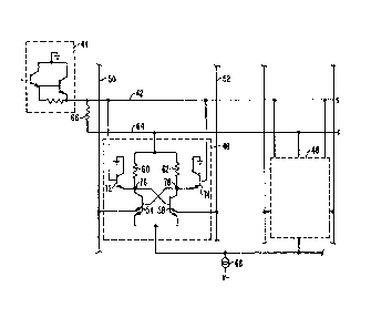
~ igure 2 is a circuit schematic of a first
embodiment of a memory cell cixcuit according to the
present invention A word line 42 is driven by a
-20 DarlincJton driver 44 and is coupled to a plurality vf
memory cells, of which memory cells 46 and 48 are
shown. Memory cell 46 is also coupled to a bit line 50
- and its inverse, bit line 52. Bit lines 50 and 52
provide the indication of whether a 1 or a 0 is stored
in memory cell 46 for the word associated with word
line 42. In a complete memory circuit, there are a - r
plurality of word lines intersected by a plurality o~
bit line pairs, each with cells as illust~ated/
Memory cell 46 has a pair of cross-coupled
transistors 54, 58 which have associated load resis-
tors 60, 62, respectively Instead of load resis-
tors 60, 62 being coupIed to word line 42 as in theprior art, they are instead coupled to a line 64 which
is itself coupled to word line 42 through a common
resistor 66.
A current source 68 provides the current to
one emitter of transistors 54 and 58, while the other
:
emitter of transistors 54, 58 is coupled to bit
lines 50 and 52, respectively. Clamping transis-
tors 72, 74 are provided with their bases coupled to
word line 42 and their collectors coupled to ground.
The emitters of transistors 72 and 74 are coupled to
the collectors of transistors 54, 58, respectively.
In operation, if transistor 54 is on, clamp-
ing transistor 72 will limit the voltage at the collec-
~ tor of transistor 54, node 7Ç, to a first voltage level
(V1). Because current is flowing through resistor 60,the voltage at line 64 will be at a second voltage
level (V2). The voltage at line 42 (V3) is equal to V2
plus the voltage drop across resistor 66. V2 is
equivalent to the voltage drop through the
transistor 72 base-emitter junction, as divided by
resistors 66 and 60, below V3. Because no current is
flowing through resistor 62, the collector of
transistor 58, node 78, is at this lower voltage (V2)
of line 64. Thus, since node 78 is coupled to the base
of transisto~ 54, the forward base-collector voltage
for transistor 54 can be limited to less than the
voltage necessary for the onse~ of saturation. This is
acoomplished by choosing the appropriate value for
~ common resistor 66.
Since a plurality of memory cells are coupled
to line 64, the value of common resistor 66 is chosen
to be approximately equal to the parallel combination
of a load re~istor ~either 60 or 62) and an equivalent
load resistor in the remaining memory cells coupled to
line 64. The value used for resistor 66 can be simply
calculated as the value of a single load resistor (60)
divided by one-half the number of load resistors
coupled to line 64. Thus, for example, if there is a
0.8 volt voltage drop across the base-emitter junction
of transistor 72, the voltage drop across resistor 66
will be 0.4 volts, thus resulting in a 0.4 volt forward
voltage across the base-collector junction of
transistor 54.
By connecting the collector node of clamping
transistors 72 and 74 to ground, a speed improvement is
achieved. This ground connection serves to ground, or
short-circuit, the substrate capacitance present at the
collector of transistors 72 and 74. In addition, by
connecting the collector of clamp transistors 72 and 74
to groundl these collectors can provice most of the
read current for memory cell 46, thus reducing the
amount of current which must be provided by driver 44.
This arrangement permits the use of smaller devices for
driver 44, thereby reducing the area required for the
driver and reducing parasitic capacitances. This
results in an improvement in performance.
Clamping transistors 72 and 74 thus reduce AC
capacitive loading by grounding their collectors. DC
loading is reduced since the collector is connected to
Vcc, or ground, and thus can provide the required DC
read current, or at least a majority of the DC read
current. By xeducing the loading of word driver 44,
the noise margin of the circuit is improved.
An alternate embodiment o~ the present invention
is shown in Figure 3. As in Figure 2, a pair of
transistors 54, 58 are provided with associated ~oad
resistors 60, 62 and clamping transistors 72, 74.
However, resistors 60 and 62 are coupled directly to
word line 42 while the bases of clamping transistors 72
and 74 are coupled to a line 80 which is coupled to a
common resistor 82. Resistor 82 is coupled between a
current source 84 and a node 86. Node 86 is an
intermediate node in a word driver 88 where the emitter
of a transistor 90 is coupled to the base of a
transistor 92.
In this embodiment, if transistor 54 is on,
the voltage at node 76 is determined by the voltage
drop through common resistor 82 and the base-emitter
32~
voltage of transistor 72. Node 78 will be at the
voltage level of word line 42 since no current flows
through resistor 62. The line 42 voltage will be
lower than the voltage at node 86 by the base-e~itter
5 voltage drop of transistor 92. Thus, this voltage drop
will be less than the voltage drop to node 76 by the
amount o~ the voltage drop through common resistor 82.
Because resis~or 82 draws current from Darlington
driver 88, a cuxrent source 84 is required to provide
10 the additional currentO
As in Figure 2, a plurality of memory cells
are coupled to word line 42 and line 80 in the same
manner as shown. The value for resistor 82 is
preferably chosen to give a voltage drop across
15 resistor 82 of approximately half the base-emitter
junction voltage of transistor 92. If the base~emitter
junction voltage of transistor 92 is 800 mill-volts,
for example, this will result in a 400 millivolt
differential between node 76 and the base o
20 ~ransiætor 54, thus preventing transistor 54 ~rom going
into sat,uration in the "ON" state~
As will be understood by those familiar with
the art, the present invention may be embodied in other
specific forms without departing from the spirit or
25 essential characteristics thereof. For example, a
diode could be used in place of transistors 72 and 74 r
of Figures 2 and 3 r respectively. Alternately, a
driver other'than the Darlington driver could be used
in Figure 3, with common resistor 82 being coupled to
30 an intermediate node. PNP transistors could be used
for the memory cell using an inverted structure if PNP
transistors with the proper size and speed are
developed. Accordingly, the disclosure of the
preferred embodiments of the invention is intended to
35 be illustrative, but not limiting, of the scope o~ the
- invention which is set forth in the following claims.