Note: Descriptions are shown in the official language in which they were submitted.
8~
E LECTR I CAL CONNECTOR
~S~
S B~ ~ I NVENT I ON
1. Field of the ~nventio~
Thl~ ~nYention r~la~e~ ~o electrical
conrlector~ a~l~iaced to printed ~:ircuit boards and,
laore particularly, to providi~ reta~ning Isean~ ~or
fiuch ~:onn~ctors whil~ ~ t~ teclainal p~llB are older~d
to th~ pcirlted ~ircult ~oa~d.
2~ D~criptioll o ~elat~d ~t
Si~ce t~e a~ven~ o~ the p~inte~ ~ircu~t
boar~, electr~cal com~on~nt~ hav~ ge~eeally bee~
a~ ea to th~ board by ~older~g the colDpoale~t l~ad6
to the pri~te~ el~tr~ical pattel:n. Of~e~ times Ule
co~pone~t lead6 ~xten~ throu~ ~he board ' ~ holes and
~u6t be old~r~d 1~ th~s po~tio~.
0~a~ o~ the problems ~couat~r~d i~ such
opeæatio~ aa~n~alni~ ~he ~o~oDe~s ~ the
de~Lr~d po~ltion or orle~t~tior~ durl~g a~se~bly aa~
~oldle~g. tlariou~ ~teen;pt~ have been made ~o 801ve
~hi~ probl2~. In earliQr ti~ when d~creSe
electl~cal co~aæonent$ ~uch 26 capa~i~ors and
~e~ t(:~r8 ~rere ~osllmonly ~f iaced in large nu~ber6 to
~ ~ pri~ted s~r~uit board~, variou8 lead lo~king
`~ a~raQge~ent~ wexe su~gestea. For ~exa~plç, in U.S.
~: : Pat~nt 2.7S4,4B6 sJ~ansQd 1956 July 10, to C. J.
~la~hocll. the two rela~ively ~of t l~ad wire6 o a
r~istoc ~ire~e tw~t~d ~A a~ conf ~qu~a~ion ~o whe
ected, ~he leads temporacily lock by hooking
around the side and edge of the board hole~, to
:~ there~y hold th~ reBi6toe ~rl pla~ wh~le 601derifag.
Dilar approache~ :were p~oposed fo~ capaci~ors ~n
~ : 35U.S. Pat~nt 3,16~,721, slranted Decembec 22, 1964,
: ~ .
. : 1
~ !
.
:
. .
.
;
.
U.S. Patent 3,056,9~9 granted October 2, 19~2, and
U.S. Pa~en~ 3,239,720 granted March 8, 1962, all to
C. C. Rayburn~ a~ ~rell a~ U~S. Patent 3,747.04~
granted July 17. 1973 t~ H. A. Stros~ here such
5 di6c~ete com~onent~ have been packag~d ~oge~her.
~imilar techniques have been tried . U. S. Patent
3,52~,108 graneed Augu~t 11. 1970 to J. A. Engli6h,
for example, disclo~e~ a board mounted modulax
~ircuit co~po~ent compri6ing a hard di~lect~c
10 ceramic ~a~erial ~upeorting a ~lumber of acti~re and
passi~e ¢or~ponel~t~ with ~ultiple, self-locking lead~
bent i~to a conf igura~io~ ~o a6 ~o provide ~am
surfaces or contacti~q the printed ~ireuit board
holes .
~etention durillg solderin~ i6 parti~ularly
important iD~ connection with the more ~ecent
rlulti-ter~ al con~leceors~ ~here 6uch ~:omle~or6
have f lat. thin lead~, which ~an be readily ~rim~ed
as ~E~ the discrete component~ of ~he pa~t, t~e
20 rete2~tio~ i 8 ~ot a seriou~ proble~ Thi~ ~ be~ause
the ~a~ily crimped f lat. thin lead~ usually hav~ a
lar~e o~feet permi~ting adequate room ts~ E~a~s throug~
the boara holes. ~he ccimped portion ~as~es
completaly through hole6 and lock~ to the other end
25 o~ ~che holes. ~rO provide adequate ~e~en~ion, the
~: thiclcnesæ o~ the board and location are ~eitlcal.
l~ the cafie o~ elec~ al connector header6,
lead locking arrangement~ of the prior ~rt are no~
easily applied. Such header6 includ~ numerous male
30 tecminal pi~ ~urrounded by vari~ufi pla~ic6. The
;oal~ pil~8 are ~ypially square metal pO8S;Ei
approximately 0.025 inches Equare and are very
~: ~tif. E~ecause of the ~ize and ~tiffne~s s~ such
~; ~ 6guare male pin~, headerfi are 601dered to printed
35 clrcuit u'cilizing rarious hold-down device~ to retain
~ '
;
: .
:
8~7
the header in place during the ~oldering opeLation.
Such d~vice~ include mecha~ical ~a~teners such a~
bolt6 and screws. ~eighted plates are al60 us2d.
These are placed atop ehe headers and re~oved a~ter
the soldering pcoce~s- ~lthough such method~ work,
they are exæensive becau~e they are labor intensive.
Wi~hi~ the last few yea~, method~ of
att~h~ent whi~h a~e an in~egral part of She he~der
have been sought. ~hat ha6 been tried typically
involve~ employi~g a si~gle male pin in the header
which will i~terfe~e with one p~inted circuit boa~d
hol~. The ~ale pin u~ed iB co~monly one of the
commercially ~ailable complia~t-eype pin~. ~uch
æin6- however, u6ually require high i~6ertion forces
on tAe order o~ ~0 pou~d~. A1BO~ they are u~eful ~or
o~e i~ertio~ only.
The ~ove to roboei~ in~ertion ha~ lead to a
~eed for a header tha~ ~an be me~hani~ally placed o~
a pri~ted c~rcuit board and automatically retai~ed
Z0 ~hrough ~ub6equent board ha~dling and ~oldering
operation~. Robotic loader~ typically ha~e an upper
it on inser~ion ~or~es tfor example, about 15
pounds3 ~o prote~t the ~ircuit board in ~6e o a
mi~placed or d~maged component. As thi~ load limit is
~; 2S leached. the inKe~io~ head oP the robotie loader re-
tract6 So pro~ide ~his safety feature. Consequently,
~; ~ retention feature6 ~u6t hæve relatively low in~ertion
orce~ to be used wiCh ~obotic loader~.
0 ~-~e~
The present inven~ion provide~ a solution
: for reeaining an elec~rical connector header in tbe
correet p~si~ion during ~oldering and other handling
opecations. The ~er~inal end of one or more eair~ of
3S male pin~ are de~or~ed or ~rimped in ~uch a manner
~ ' ,
: 3
- .
;
. . .
E328~
that they operate in conjunction with one or more
pair6 o printed circuit board holes to retain the
entire header in the correct eosi~ion during
~oldering. Becau6e the pin~ are ~hick and ~tîff,
S ea~h pair of deformed pin~ provide very high normal
force~ again6~ the in~ide of the corre~ponding pair
of opposinq printed circuit board holes into which
the pin~ are ~nserted. A16D~ location of the ~rimp
i6 ~ot dependant upon thicknes~ of the printed
~ircuit board because retention depe~d~ upon the
co~ple~enta~y n~r~ orce~ o~ a paie o pin~ again6t
two op~o~i~g printed ~lreuit board hole~. The
comple~entaly a~tio~ of ~ach pin of the pair a~ainst
the corre~pondi~g ~urface of . tAe hole provides
lS retentio~, no ~a~ter vhether the board is rel~tiYely
thin or thiek. A1BO~ the thick pins allow for very
littl~ roo~ for offsee without crea~ing very hiqh
inse~tion for~e~
BRI~F D~S~RIPTIO~ OF rHE D~AWINGS.
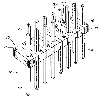
FIG;. 1 i~ ~ I?e~Bpec~ive view of a f ir6t
: ~ e~bodiment of the pre~e~t invention illustriting a
pair of ~ri~pad ~etaining pins in a double row
. vertical header.
~G. IA i~ a ~op view of PIG. 1
FI~. lB i6 a ~e~tio~al view taken along the
line B-B of F~G. lA, a~ter in~er~ion in a printed
circuit bo~rd~
FIGS. 2~ 2A and 2~ are re~pe~tively
30 ~i~ilarly ~iews of a ~econd embodiment o ~he pre~ent
~: ` inveneion illu~trati~g a pai~ of crimped retaining
pin~ in a Sriple row verti~al header.
~ IG5. 3~ 3A, 3B, and 3C are al60
respecti~ely 6i~ r views of a t~ird embodiment of
: 35 the presen~ invention illustra~ing two pairs o~
'
~: 4
~: :
~32~
crilaped r~taining pin~ in a single row veLti~a
header .
~ IGS. 4, 4A, and 4B are al60 re~pectively
~imila~ view~ o ~wo pair~ o~ crimped pin6 in a
S 6ingle row. ~ight angle header.
FI~S. 5, 5A and 5B are a 160 cespe~tively
~imilar view~ of a eair of crimped retaining pin~ in
a double row, righ~ allgle head~r.
DESCRTPTI~
P'IG~ 1 illu6~rates a first embodi~ent of the
pre~e~t inverltion wherein a ~oubl~ row ~rertical
header 10 i8 ~;IIOWll. The header compri~e~ t~o row~ of
6quare male termillal pill~ 12. Such olale ter~ al
15 pin~ are a~ indu~ry s~andard 0. 025 i~he~ ~quare.
The pitl6 ar~ held in a pla6ti~ retai~er or
wafer 14. In FIG. 1, a pair o~ ad~oining pi~, 12A
and 12~, hav~ ~ee~ crimped a~ 6~10WD~ at the~r ter~inal
or inser~ion end. I~ the e~bodilse~ howll, the
20 de~or~a~on i6 su~h ~hat the cri~ped por~on~ of pill~
12A and 12B extend toward ea~h other. The re'celltioll
~eatur~ of the present in~re~ltion wil~ worlc equally
well if ~he cri~Dped por~ion6 both exterld away ro~
each other. What i~ im~orta~t ~8 that each crimped
portion o~ ~he pair cooperate against c~r~esp~nding
~urfaceg in the ~rinted ~ircui~ board hole~, a~
explained belo~. Buttons 16 ase ~rovided on the
wafer 14 to provide an offset between waSer a~d
printed eireuit ~oard ~er insertion o~ the header
30 10. This allows for ad~quate cleaning a~ter ~he
~oldering operi~ion.
PIG. lB illustrates the r~tention acCion of
the pai~ oS cri~ped pins 12~ and lZB after the header
10 is in~erted into a printed circuit board 18. The
35 cri~ped end o~ the ~ina ~re ahown ~ithin the holea of
.
'
. ~ ~
.. ~ .~ .
the board. It ~hou1d be noted that re~ention can be
achieved by ~ontact of the ~rimped portion of each
lead wi~h only one side of it6 hole at points
idenei~ied a~ l9A and 19B, respecti~ely. The normal
5 focce~ exerted agairl~ h~le ~urface6 19A and l9B by
the crim~ed portion of pin6 12A and 12B i~
8uf f iciently high to providQ the neces~ary letentio~
du~;ng the ~older;ng opera~ioll.
Since only one 6ur~ace of each hole 3.6
10 l~eces~ary fo~ retentiorl. the thi~kness of the pr~lted
circuit board iB not a~ ~ritica1 as where retentio
due to a terminal or lead de~or~atiorl requir~
~ontact with oppo~ite 6ide~ o~ the ~al&e to ~ircuit
board ~ole. Thus the pre~ent inve~io~ operate~
15 equally ~ell in very thin asld ~rery ~hi~k l?rin'ced
circuit board~. ~hat i6 i~po~taalt i8 that at l~ast a
pair o~ co~ple~entacy pins be 6imila~1y cri~ped ~o
that normal force6 of the c~i~pe~ ~oreion o~ ea~h act
coope~ati~rely agai~st the 3~orres~ond~ ~g 6urface of
20 ea~h re~pecti-te prineed car~uit board hole.
FIGS. Z, 2A ~r~d 2B illu~teate a ~eco~d
er~bodi~ell~c o the pre~ent inYention where 1~ke part~
ar~ identif ied by the 6ame reîereD.ce sluD~ber ~ Thi~
second embodimer~t ~hows a tciple row verti~a1 header
2~ 2D dif~ering ~om header 10 es~en~a11y o~ly in that
it contain6 three ins~ead of two rows of pins 12. A
~;in~le pair of ~rimpe~ termina16 12A and 12B i~
utilized h~re al~o, one from ~he fir~t a~d third
row~. They aee separated by a regular pin 12. The
~o cetentiol~ action in the p~inted cirouit board 18 i~
otherwies identica1 a~ ~how~ P`IG. 2B.
PIGS. 3, 3P. and 3B illu~ra~ a third
embodimen~ of the present invention. The header 30
in ~he embodiment compr~e~ bu~ a ~ingle row of einfi
3~, held in a pla~ wafer 34 ~imi1ar to 14 o~ the prior
er~bod iments .
~3L2~3;28~
since only a ~ingle row i8 u~ed, the
retaining pin~ with crimped end~ mu~t be in the same
~ow. In the embodiment of FIG. 3~ two pair~ of pin~
aee ~rimped in alternating dire~tions. One pair o~
oppositæly cri~ped pins, however~ will al~o p~ovide
adequa~e retention. Paî~ 3~ and ~2B cooper~te with
one another as do pairs 32C and 32D in a m~nner
similar to the ~ingle eair o ~rimped ~in6 in the
~ir~t two embodiment6 to pro~ide re~ent~on of the
header iQ the printed cir~uit board. ~hu8. a6 BhOW~
in PIG. 3B. co~ple~entary crimped ter~als 32A
(shown ~n solid) a~d 32~ (~hown ~ phanto~ have
~heir cri~ped po~tio~ exerti~ ~or~al ~orce~ agai~6t
oepo~ite 6uraces of their re~pective pri~tea ~ircu~t
board hole~. thereby a~hie~ing the sa~e retention
actio~ a6 in the peio~ e~bo~i~ent~. Likewise, the
6ame ~ B true ~oe cri~ped termi~al6 32C ~solld~ a~d
32C tPhantom) s~owu ~ ~IG. 3~.
FI~:S. ~, 4A a~d 4B il~UBtrate a fourth
em~odi~ent of the pre~ent ~nve~tio~. The ~eader qO
i al60 a si~gle ro~ header but the ~ermi~al pin6 42
are ben~ a~ right a~gles at one end. ~hi~ i~ becau6s
heade~ 40 i8 desig~ed to be ~serted into ~rinted
circui~ board ~8 a~ riqht a~gle~ as shown in
25 ~IG. 4C. A~ before, the pin~ ~2 are h~ld by a
pla~tic wafer 44. ~ader ~0 al60 has two ~air~ of
pin8 cri~ped alternatively as in th~ header of
~IG. 3~ ~e ~rimp~ a~e ae the ri~ht angle poreion o~
the pin~ for obviou~ eea~on~. Thus, afi ~n the ca~e
30 o~ ~he embodiment of PI~. 3, pairs. 42A and 42B and
pair6 42C and 42D of c~i~ped terminal~ cooperate to
retain the header in ~he pri~ted circuit boa~d g8.
FIG. 4B ;lluserate~ the previou61y explained
cooperative retaining action be~ween crimpe~ pin 42B
35 (solid) and 42~ ~phantom~. ~he Bame oc~ur~ ~n the
~x~
- ca~e of pins 42C and 42D. Again, ~dequate r~tention
can be obtained with a single pair of crimped pins~
~ IGS. S, SA and SB illu~trate a fifth
emb~diment of the pre6en~ invention. The header6 50
5 is a double row, right angle header, m0aning that it
compri~es a double row of pis~ 5~ held by a wafer 54
where all th~ pins are set at righ~ angles for
insertion into a prineed ~:ircuit board. A pair of
pins 52P, and 52B are ceimped irl th@ manner previously
10 de~crib~d. Thu6, when the header 50 16 in~er'ced i~to
the printed circuit board 58, ~rimped terminal~
cooeerate as did crimped pin~ 12A and 12B io~ the
embodime~t of ~1~. 1 to reta~ header 50 in .~e
prope~ positio~ during 601deriny.
I~ i6 to be url~er6tood that the orlDs of ehe
invention 6how~l and deEcribed herei~ are ~ut preferred
embodiment~ and the variou~ ~hange~ ~ay be ill that
departinsJ ~rom the spirits and s~ope of the in~e21t~0n.
~5
'
:: i
: 35
: `:
,
,