Note: Descriptions are shown in the official language in which they were submitted.
1~3;~4
TIN-SOLDERING MACHI~E WITH P~UTOMZ~TIC WAVE
BARRIER FOR PRINTED CIRCUIT BOARDS
BACKGROKUND OF THE INVENTION
1. Field of the Invention
An object of the present invention is a tin-soldering
machine with an automatic wave barrier for printed eircuit
boards.
2. Description of the Prior Art
In electronic industries, where printed eircuit boards
are mass produced, components are soldered by the so-called
"wave" soldering process in which a turbine maintains a
constant output of molten lead-tin alloy that flows out
over a spout with a specific shape.
The shape of the surfaee of the molten alloy, its
flowing-out speed and its cleanness are major factors that
determine the quality of the solders.
The geometry of the eleetronie board is also a
determining factor: ideally, the board is flat and, in its
translational motion, it approaehes a rectilinear
generating line of the surfaee of the molten alloy.
In practice, boards are not flat and have a tile shape
whieh beeomes accentuated with increasing width. The molten
metal generating line is not reetilinear either, and its
surfaee may be spoiled by dross.
It will be understood that, if the board to be
1~83;~
soldered has a tile shape with downward convexity, there s
a very great risk that, during the approach, the molten
metal will flood the components side of the board which
will then be irretrievably lost. If a compromise
setting is attempted to avoid this problem, there is the
risk that the components will not be soldered.
These reasons lead to the use of costly remedies,
among them:
- the addition of stiffeners to the electronic board
itself. If the board contains power elements, the rigidity
of the metallic radiators could be taken advantage of;
- or, more generally, a soldering frame is used, in
which the circuit is confined and which combines the
functions that the electronic board cannot fulfil by
itself, especially the wave barrier function.
SUMMARY OF THE INVENTION
An object of the invention is a soldering machine made
so as to avoid any excess cost related to the board, or any
additional manufacturing operations such as the placing of
the board in a frame and then its withdrawal after
soldering.
The soldering machine according to the invention has a
wave barrie~ device which is rigidly joined to the machine.
According to an advantageous feature of the invention, the
wave barrier device has a part which brings down the level
1~33;~4
of the tin wave crest locally, just before the arrival of
the leading edge of the board to be soldered.
According to an ad~antageous feature of the invention,
the wave barrier device has a blade made of a material that
does not melt at the temperature of molten tin. This blade
penetrates the surface of the tin bath before the leading
edge of the circuit to be soldered.
BRIEF DESCRIPTION OF THE DRAWINGS
The present invention will be better understood from
the following detailed description of an embodiment, taken
as a non-restrictive example and illustrated by the
appended drawings, of which:
- figure 1 is a simplified and partial side view of a
soldering machine according to the invention, and
lS - figures 2 and 3 are enlarged views of details of the
soldering machine of figure 1 at two different instants in
the passage of a printed circuit board.
DESCRIPTION OF A PREFERRED EMBODIMENT
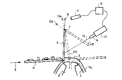
Figure 1 is a schematic view of that part of a tin
soldering machine which is at the tin wave 1. The term
"tin" herein refers to any appropriate meltable soldering
alloy or product that contains tin but not exclusively tin.
The tin wave 1 is produced conventionally, using a nozzle
2. This wave 1 can be poured symmetrically upstream and
downstream of the nozzle, as shown in the drawing, or else
3~
it can be poured non-symmetrically. An arrow 3 indicates
the direction in which the machine conveyor moves. This
conveyor carries printed circuit boards, provided with
their components, such as the board 4 shown in the drawing.
The relative positions of the conveyor and the nozzle are
such that the upper side 5 of the tin wave 1 is at a higher
level than the upper side of the board 4. This makes it
necessary, with prior art machines, to have wave barriers
placed in front of the boards (or supporting frames fitted
with front walls acting as wave barriers) to prevent the
upper side of the board from being flooded by the molten
bath.
According to the invention, a movable wave barrier is
placed on the machine. In the embodiment shown in the
drawing, this wave barrier has a flap 6 which is mounted to
be movable rotationally around a pin 7, from which it is
suspended. This pin 7 is parallel to the planès of the main
sides of the flap 6 and is perpendicular to the direction
in which the conveyor moves. The flap 6 has a substantially
rectangular shape and its width is substantially equal to
the width of the board 4. In its idle position (shown in a
solid line in figure l), the flap 6 is placed in such a way
that its lower lateral side 8 is at a distance D of
approximately 2 to 3 mm. above the level of the lower side
of the board 4, this side being therefore below the level
1~3~4
5. The pin 7 of the flap 6 is placed so that it is roughly
perpendicular to a line A (of whlch only a point is shown
in figure ~) which can be defined as the position that
would be occupied by the leading edge B of the board 4 (the
lower edge of the front side 9 of the board 4) on coming
into contact with the wave 1 if the flap 6 did not exist.
A position-marking device 10, that works together with
a position sensor 11, is fixed on the upper part of the
flap 6. This sensor 11 may be either an optic type of
sensor or an electromagnetic type of sensor or any other
type of sensor. The sensor 11 is connected to a device 12
for the processing of data from the sensor and for the
control of a jack 13 placed downstream of the flap 6. The
making of the device 12 will be obvious to those skilled in
the art from a reading of the present description, and
depends on the type of sensor 11 and jack 13 used. The rod
14 of the jack 13 is connected to the flap 6 by means of a
flexible connection 15, such as a chain or a cable. When
the jack 13 is actuated by the device 12, it pulls the flap
downstream (i.e. towards the right in the drawing).
The working of the machine described above is as
follows. In the idle state, with the flap 6 in the position
represented by a solid line in figures 1 and 2, the
conveyor approaches the board 4 until it makes contact with
the flap 6. With the conveyor continuing to move forward,
the board 4 pushes ~he flap 6 along a length L of
approximately 1 to 2 cm. without anything happening.
As soon as the board 4 has travelled the length L, the
flap 6 reaches the position marked 6A in figures 1 and 3,
5 and the position-marking device 10 reaches the position
~arked lOA. At this moment, the signal given by the sensor
device 11 reaches a pxe-determined threshold set in the
device 12, thus making the latter excite the jack 13 which
withdraws its rod 14 and thus pulls the flap 6 through the
link 15. The characteristics of the jack 13 and its
control are such that it moves the flap away in the
downstream direction at a speed greater than that of the
movement of the board 4. The jack 13 moves the flap away up
to a position 6s (figure 1) such that the said flap can let
the board 4 pass through without any risk that its
components will touch the flap.
When the flap 6 starts moving from the idle position
to the final position 6B (so long as it i5 in contact with
the tin wave) pushes back the tin practically in the same
way as would a conventional wave barrier. When the flap 6
moves quickly away from the position 6A towards the
position 6B, it pushes the tin by creating a moving dip in
the tin. This dip precedes the board 4 and prevents it from
being submerged. The crest of the wave that foliows this
dip wets only the lower side of the board 4, depositing the
solder at the requisite places.
The distances D and L, as well as the level 5 with
respect to the level of the board 4, and the withdrawal
speed of the jack 13 are set experimentally so as to
provide for the optimum soldering of the leads or
attachments of the components of the board 4.
The movement of the flap 6 also has the effect of
pushing away, from the board 4, any dross 16 which might
occur on the surface of the tin wave~ A device (not shown)
which can either detect the end of the passage of the board
4 or be activated at the end of a time lag, controls the
outgoing of the rod 14 of the jack 13.
According to an variant (not shown) of the embodiment
described above, the flap moves in a rectilinear
translational movement while remaining substantially
perpendicular to the direction 3 and then, when the board 4
is sufficiently engaged in the wave 11, the flap is lifted
in a direction perpendicular to the direction 3 and then
brought back to its "idle" position (the same position as
in figure 1, but in this case, we could have D = 0) after
the passage of the board.
~ ccording to another embodiment of the invention, the
flap is replaced by a movable nozzle that blows hot inert
gas. This nozzle creates a "curtain" of gas ]ust before
the board 4 which it precedes and this curtain of gas
3;~
produces a dip in the surface of the tin wave, preventing
the tin from submerying the board.
1~
~5
. ' ~
:' .