Note: Descriptions are shown in the official language in which they were submitted.
20163
MASK ASSEMBLY HAVING MASX STRESS RELIEVING FEATURE
CROSS REFERENCE TO CO-PENDING APPLICATIONS
In co-pending Canadian patent application Serial No.
519,971-9 ("Mechanism for Automatic Precise Regis~ration
of Shadow Masked EL Electrode Patterns", Boudreau et al.),
there is defined a mechanism that allows for remote
controlled total automatic registration of shadow masks to
a substrate while being operated in an in-line deposition
system.
In co-pending Canadian patent application Serial No.
519,973-5 ("Mask for Patterning Electrode Structures in
Thin Film EL DevicesU, Robert Boudreau), there is defined
a mask structure and a method of fabricating electrode
structures for a thin-film EL device that utilizes such a
mask structure.
Both of the above applications are filed concurrently
herewith and are assigned to the same assignee as the
instant invention.
TECHNICAL FIELD
The present invention relates in general to thin-film
display panels, and particularly to a mask assembly and
its use in the fabrication of thin-film structures for a
thin-film device.
BACKGROUND OF THE INVENTION
Thin-film display panels (such as LCD or
electroluminescent) have been known to be very useful for
displaying information inasmuch as the thin-film
structure, including the cross electrodes, can be
~5-1-098 -2- PaTENT
~epo6ite~ o~ d gla86 substrate ther~y providi~g a ~atris
di~play panel c~pable o~ be~g ~el~c~iYely ~ergiz~ to
activ~te ind~vi~ual pi~els thereon. One of the problems
en~ountered in the Danufacturing o~ thin-f il~ display
panel~ i~ the development o~ proces6e~ that patter~ ehe
thin-film electrode structure~.
~ 08~ t~in-~ devi~es have ~ad t~eir th~-fil~
electroae 6tructure~ patterned either by a wet proce
~no~n a~ pho~oliehograp~y or by ~hado~ ~a~ing.
1~ Pbotollthography ifi very similar to ~roce~se~ u6ed to
develop photographs i~ that the depo~it to be patternea i6
coated with light-~ensitive ~aterial, w~i~h i~ then
exposed to a negative or a positive pattern and then
developed and later 6tripped in ~arious corrosive
developing solutions. T~e disadvantages of this ~ethod is
tha~ it i~ ~lov and labor inten~ive. and i~Yolve~ Dany
step~. ea~h one sub3ect to failure or pos~ible
Dta~ination of th~ thin~ device. - -
~it~ respect to the use of ~hado~ na~ing to depo~it
thin-fil~ ~tructures, re~erence i6 ~ade ~o U.S. Pate~t
4,335,161 to Pang C. Luo, entitled ~'THIN-~ILM T~ANSISTORS~
THIN-PILM TRANSISTOR ARRAYS AND ~ P~OCESS POR PR~PARING
TKE SA~E~. In ~ummary, t~e Luo patent appear~ to di~clo~e
a ~ethod vf prepari~g a thin~ tran~i~tor or an array
~ thin-film tran~i6tor~ by depo6iting in vacuu~ the
di~ferent component~ through a ~ingle apertured ~ask
~herein the ~apertured ~a~k i6 moved in a predetermined
pattern for the depo~ition of each of the ~o~ponent6. I~
t~e proces~, 6emiconductor ~aterial i6 depo~ited through
the ma~k and ~hen the ~a~k i~ moved in a direction a
di~ta~ce eguivalent to the lonqe6t di~eD~ion of the
as-l-o98 -3- PATRN~
opening6 in t~e ~a6k. T~rou~bout the tbin-f 11~ tran~lstor
foraation proce~6 the ~a6k i6 ~OYca ~everal ti~es in
~ifferent ~irection6. The ~6e~bly thæt i6 then forme~ i8
re~oved ~rDm t~e vacuum and ~he fabri~ation co~pleted by
technique6 ~uc~ a~ photolit~ography.
A~ in Luo. 6hadow ~aski~g i6 u~ually peror~ed over
~all 6u~6trate~ wit~ 6ti~f ~a6~ at are manually
cla~pad to en6ure eve~ ~ontac~ wit~ a particular
sub6trate. This i~ ~ relatively 610~ proce6s ~nd u6ually
require6 breaking vacuum in the depo6ition ~hamber,
re6ulti~g in ~o~e thi~-film contamination. ~en
depo~iting t~rough a large area ~as~ co~mon t~at
the ~ubserate i~ not perfectly flat or ~ot level with
re6pect to its surroun~i~g sub6trate ~older. The pre6ent
lS inve~tion addre~es t~is and o~her proble~ ari~ing from
the difficultie~ of remote auto~atic handling o~ large
area shadow ma~k~ in in-line ~eposi~io~ ~y~tems.
~ A ~ethod whi~h ~ould produce thi~-fi-lm structure6
wit~out the use of p~otolithography would be considered a
~ignifieant adva~cement in the thin-filD 6tructure
depositio~ art. I~ additio~, it i~ al~o believed that a
mechani6~ ~hich ~ould ~upport the shado~ ~a~k while
relieving ~tresc i~ the ~a6k duri~g depo~ition would
~onstitute a ~ignificant advancement in the art.
DISCLOSURE OF THE INVENTION
~ t i~ therefore a primary object cf t~i6 invention to
enhance the art of ehi~-film 6tlucture depo~ition and
partic~larly that art involving thin-film display panel~.
It i~ another objeet of t~i~ inve~tion to provide a
~a~ as~embly for patterninq thin ~ tructure~ in
thin-fil~ ~evice~, particularly electrode struct~re6 in
di~play panel~.
~5-1-098 -~ PAT~NT
Still ~ther ob~ect of the ~nve~tion 1~ to proYid~
~et~od of depo8~ tin~ a patter~ of e~ectro~e ~tructurss,
wber~in t~e ~et~od i~ol~E th~ u6e of a ~a~k a6~bly
~aYi~g ~ ~ean6 of ~upporti~g t~e ~as~ ~uring depo6itio~
w~ile relieving ~tre~ on the ~a6k.
In accordance with one ~6pect of tbi~ in~entio~, there
i6 proviaed a ~a~k ~e~bly for pa~terni~ thin-fil~
str~cture6 ~or a thin-fila device having a$ lea~t a
substrate. ~e ~a~ a~sembly compr~ ~e8 a ~etallic ~nner
6hadow ~aEk portion having a predeter~ined pattern of
~pertures wit~ a border portion di~po6ed about the
aperture~ addition, a ~etallic outer ma~ portio~ i6
looated about and coplanar with the inner ~a6k portion.
~inally, the ~a~k as~embly includes mean~ for supporting
the inner ~hadow ~as~ portion ~hile relieving ~tre66 i~
the inner ~ask portio~ during depo6i~ion of the thin-film
struoture~. the ~upporting ~ean6 di6posed between and in
operative ~ontact ~ith the inner ~nd ~he outer ~ask
portion~.
- In accor~ance with another aspect of t~i~ invsntion,
there is provided a ~ethod of depo6iting a pattern of
thi~-fil~ st.ructure~ for a thin-fil~ device having at
lear~ ~ ~ub~trate. ~he ~ethod eompri6e~ the ~tep6 of
providi~g a ma~ a~e~bly compri6ing a metallic inner
6hadow ~a~k portion ha~in~ a predeterained pattern of
25 aperture~ h a border portion di6po~ed about the
aper~ure~, a ~etallic outer ~ask porti3n located about and
~op~anar with the inner shadow mas~ portion and ~ean~ for
supporti~g t~e inner ~hadow ~a~k portion while relie~ing
~tres~ in the inner ~hadow ma~k portion during depo~ition
of ~ne thi~-fil~ ~tru~ture~. t~e 6upporting ~eans di~po~ea
bet~ee~ and in operative contact wit~ the inner and outer
as-l-09~ -5- PA~NT
~as~ portion~. 'rhe ~etho~ ~urther ~o~pri~es the ~tep~ of
po6itioning t~e ~a~k a66e~bly on one s~e of the substrate
and po~itioning a ~a~net ad~en~ ~he s~de o~ the
~ubctrate oppo~ite ~he ~a61~ as~e~bly such that t~e inner
611aaow ~a61c portion i~ ~leld in operati~re contact wit~ the
5 ~ub~rate ~ditl~out ~au~ing 8tre8~; on the inner ~Gask
portion. Pinally, ~he method in~ludes ~be step of ~acuu~
depositin~ a thin~ ;tructure IDa~erial through the
apertures of the inner ~aslc por~ion, t~ereby $0r2inSI the
t~in-film ~tructure6 on ~che 6ub6trate.
BR IEF DESCR I PTION OP TE~E DRA~INGS
~ IG. 1 ills~trate~ an example o~ a 6hadow ma6k which
can be used a~ part of the ~a6k as6embly of tlle pre~ent
inveation;
FIG. 2 i~ a photograph illu6trating one example of a
~na~k a~embly for supporting a zlta6~
~ IG. 3 is a figure of an enlarged se~tional viev of
the ~a6k illu~craeed in ~IG. 1:
PIG. 4 i~ an enlar~ed ~ectional view of a portion of
PIG. 3;
PIG. 5 i~ an enlarged illu~tration of the inner ~ask
portion of the ~ask assembly of ~IG. 2 in operative
contact ~ith a ~u~trate; and
PIGS. 6A and 6~ are examples of a ~ecAanis~ or
suppO~eing the shado~ ~as~ against the 6ubstrate and
placing 6uch a ~echani6~ in a ~puttering system,
respecti~ely.
~5-1-09a -6- P~EN~
~ r a better under6tanal~g of t~e pre~e~t invention,
~oye~er witb ~tber and urther ob~ec~6, ~dvantage~ ~nd
capabilltie6 thereo~. refere~ce is ~ade to the following
di6clo6ure and appended claim6 i~ ~onnection vith the
above-described dr~wing6.
The teac~ing~ of the pre ent invention addre66 a new
probleo t~at ~a6 ~ri6en from the difficul~ie~ of remote
auto~ati~ handling of large area 6hadow ~aLk~ in a~
in-line vacuum depo6ition proce6s. The present iAvention
invol~e6 tbe ~eparativn o~ the ~asking a~em~ly into two
co~ponent~. one that ~olds the 6hadow ~a6k and another
that doe6 the patterning (i.e., the ~hadow ma~k). Becau~e
the part that does the patterning i6 ~tructurally relieved
fro~ the oompone~t that holds the ~ask, t~e ~a ~ lay6 down
and ~onform~ ~o the ~ub~trate, producing a well-defi~ed
pattern. ~it~out t~is separation, a blurred pattern
re6ult6 despite very di~ficult ~nd careful align~ent by
tbe ~asking ~echani6m o~ the ma~ and 6ubstrate. Hith
thi~ ~eparation, ~echanical align~en~ i~ no longer a ~ajor
fa~tor andirepeatable, well-re~olved pattern6 can be
depo6ited. ~rin~le~ iD the ~aeterning portio~ of the ~a
a66e~bly of only ~ few thou~andt~s of an inch produce
unacceptable blur6 ~nd 6hort~ between thin-film 6tructure6
that ~erve a~ electro~e6. Thin-film electrode~ for
thin-film device6 are al~o difficult to patter~ due to
their geometry. The electrode& are u6ually very nu~erou~,
typically about SOO to lOOO in a pat~er~ and are 6paced
only a few thousandth6 apart, carrying potential~ of
hu~dred6 of volt6 dif~erent ~rom each other and having
B5-l-098 -7- PA~EN~
~lectrode le~gth~ o~ ~ve to ~e~ ~n~bes. I h~ve
~iLco~ered t~at by struc~urally rellevln~ ehe ccnter
patterning portio~ of e~e ~a6~i~g ~se~bly fro~ its outer
~ecban~c~l ~ounti~ area, DO~ 0~ the ~ficultie6 ln the
~a~ ~onforming to the sub~trate ~o obtai~ good patterns
are eliminated.
~ ith particular 4ttentio~ to FIG. 1, there i8
illu~tr~ted a s~adow mAsk lO whi~h i~ typically u~ed in a
depo~itio~ proce~6 to form thin-filD 6~ructure~ in a
t~iD~il~ devi~e. The type of ~ask utili2iny the
teac~ings o~ the pre~ent .inventio~ i6 typi~ally comprised
of a thin s~eet of ~etal havi~g a predetermined pattern of
aperture~ throug~ whic~ the thin-fil~ structure material
i~ to be depo~ited. In the pre~ent invention t~e example
of a ~hadow ~a~k u~ed i~ a ~a~k havi~g a pattern of
aperture~ for t~e purpo~e o~ ~oraing thiD~ 6tructures
in aa electrolumine6cent device. ~ask lO i~ co~pri6ed of
a border portio~ 12r~ and elect~ode-~ormi~g p~rtion 14 and
a~ electrode pad formi~g portion 16. Shadow ~a~k lO is
~ade from ~ homogeneou~ piece of ~etal stock t~at ha~ been
et~ed u~ing a photolithograp~ic ~et~od.
~ ith re~pect to PIG. 2. tAere i~ illustrated a ~a
a66e~bly 20 ha~ing a ~hado~ ~ask a~ part thereof. ~a6~
a~e~bly 20 i~ compri6ed of a ~etallic inner ~hado~ ~ask
portion 2~ having a predeter~ined pattern of aperture~ and
a ~order portio~ di~posed about the aperture~ (e.g.. ~28
lO); a ~etallic outer ~a~k portio~ 24 located about and
coplanar ~ith in~er ~a~k portion 22: and ~ean6 for
6upporting the inner ~a~k portio~ 22 while relievi~g
~tres~ in the inner ~as~ portion duri~g depo ition of
t~in-fil~ structures. the supporting ~ean6 di~posed
betveen and i~ operative ~on~act ~ith ~he inner and outer
~ 5~1-Q~ 8 -8- PA~NT
maok po~lon~ 6upl?0rtlng ~e~n~ of ~ask aD~bly ~0
inclu~ lot ~n~ 26 and oonn~ctirlg m~aro 28, ~lot ~ean~
2~ ~xt~ndlng peripher~lly about t}l~ inner m~X portion 22
~nd ~onn~ctln~ mear~ ~8 di~po~ed bet~e~n and ln contact
with inn~r ;lla6~c portlon ~2 and outor ma6k portlon ~4.
Ma~h asse~bly 20 lllu4trate~ ~n exa~pl~ of how a ~h~dow
mae~ can b~ ~upport:l3d ~ ~he ma~k ~ to b~ po~itlon~3d
adjac~n~ a ~ubQt~at~ wh~n a p~ttarn 1~ to bR dapo~i~ed or,
th~ sub~trat~. FIG. ~ aloo illu~trate~ mount$ng hole~ 30
wh~ch ald in ~pportlng ~sk aY~ ly 20 when u~ed wlt~
d~positlorl aqu~ pment in a ~Qpo~ition ~oc~
~ lth resp~ct: to 6upportlng me~n~ o~ k ~e~ly 20,
~ot ~oan~ 26 inclu~eo at 1Q~1; a thin, na~row ~lot etohed
in ~a~k ~se~nbly ~0 hatween borde~ por~lon 12 o~ lnner
mask portlon 22 and outer ma~k portior~ 24, the slot
extendlng ~æub~ntially a~out tlle p~r~ph~r~ of ~he ~nn2r
n~a~3c portlon ~ ~see FI~. 2) . In F~G. 2 connq~ing m2ara~
2B lnolude~ two ~talllc s~ nt~ a~o~ning the ir~ner m~k
and the OU~ ek portlon~, eA~h of th~ lllc ~ n~-.
dl~po~ed withln slo~ mean~ 2~ ~nd on oppo3~te ~idee o~ ths
inn~r ~ k po~tion. In ~notner em~odiment o~ co~ t~ng
~eans 2~ it 1~ posoib~e to hav~ a~ a ~$ngle ~netall1c
~egmen~ ad~oining the lnner m sk arL~I the aut~r ~ask
portions, th~ ssgment being dispo~ed withln ~lot means
26. rt 1~ pos~ibl~ to vary th~ dim~n~ion and number o~
~lots t~t can b~ ~tch~d into the m~sk a98~1bly to
inqr~ the ~reedom of the inner ma~k po~tion ~
~urt~er. One ao~ld ~l~o uea a perm~nent ou~r mask ~hap~d
rlxture ~o tha~ a ~par~te ilmer m~X m~ght be bonded to
it a~ snly two emal 1 pcint, ~h~reby ellmlnating thQ need
~o ~tC:tl a 8~ in t~o metal portlon of the m~sk ~8embly
~urrour~d~ng the inn~r m~s~. In ~re~y varia~ion, how~ver,
PATeN~
~re i~ ~e ba6~0 reguir~e~t of a ~eparate ~echanically
el~eYe~ er aa6k ~ro~ lt~ outer ~a6~ ~ort~on that ~8
rigi~ly ~t~ache~ to the ~epo6ition eguip~ent.
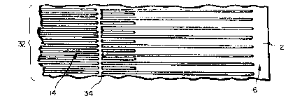
Referri~g now ~o FI~S. 3 throug~ 5, the6~ igure6
illu~trate enlarged sect~on6 of ~a~ 10 for p~rpo6e~ of
illu~trating t~e 6tructural e~peet6 of ~a~k~ of thi~
type. FIG. 3 illu6trates more ~1~6el~ border port~on 12,
~le~trode-for~ portion 14 a~d elec~ro~e-pad-forming
por~io~ 16. Ma~k 10 ~tructurally i6 ~o~pri~d of a
plurality of ~etallic ~trip~ 32 ~Dd a 6erieE of
interconnecting arched bridgefi 34, that ~erve to defi~e a
predetermi~ed pattern of ~longated aperture~. B~rder
portion 12 ih di~po~ed a~ou~ and i~ i~ eontact with
~etallie 6trip~ 32. ~IG. 4 illustrate~ an enlarged
ver~io~ of 6uch ~trip~ 32 ~ith interconnecting bridge~ 34
and elongated aperture~ 3~ PIG. 5 illu6trate6 the ~anner
in ~ic~ 6trip~ 32 are ih operative ~oDtact ~ith a
6ub~t~ate 38 ~hen æ~ado~ ~a~k 10 i6 po~itioned i~
operative contact with æub6trate 38. I~ additio~,
interconnecti~g arc~ed bridge~ 34 pro~ide 6uppore ~or
strips 32 w~ile bei~g ~paced from the $urface of ~ub~trate
38. PIG. 5 al80 illu~trate~ ~ow the ~hadow ~ask ca~ lay
1at again~t t~e 6ub6trate if it i~ flexible with ~espect
to the outer ~a~k portio~.
Il~ forming Yaa~k a~embly 20 a ho~ogeneous piece of
25 metai ~tock i.~ etc~ed u6ing photolithographic type
teoh~igue~ eo form ~he ~a~k a~e~bly illu~trated in F'IG.
2 . Both inrl~r and outer ma~k port ions are ~ade ~t the
same time ~ith orle etching ~tep. I~ foralling the
particular ~a~k~
85 1-09~ ~10- PATZNT
illu6tr~te~ IGS. 3-5, ~ d~fferent~l etch ~ u~ed
~hic~ consi~t~ of e~chi~g halfway throu~h a ~talli~ ~heet
~ith a pattern of bri~ge~ ~rom one ~ide, a~ half~ay
t~rough a ~etallic ~eet wi~ a ~etal pattern lac~inq
bridge~ fto~ t~e ot~er ~ide. Thi~ open~ up the area~
under and around bridge~ 34 with ~ 6tructurally rounded
profile ~FI~S. ~ and 5~. Si~ce ~a~k 10 i6 ~a~e feo~ a
single ~etal 6heet (~ee FIG. lj. it will not del~inate
and t~e ~a~k can be ~ade of ~ateridl6 which ther~ally
~t~ e expan6ion propertie~ of the 6ubstrate on which
the t~in~film ~tructure~ are to be dsposited. In
addition. the 6ingle ~etal ~ask can be ~ade to be
che~ically reEistant or to be magnetically attracted.
5hado~ ~as~ 10 can provide a rounded pro~ile to the Ehape
of the material to be depo~ited on the ~ub~trate and vill
allo~ for a 6ingle, ~i~ple pa~erni~g prooe~6 when
co~pa~ea to photolithography.
- ~eferring ~ow to FIGS. 6A and 6B, i~ ~IG. 6A there i6
ill~strated a aa~ rega6tration ~echanis~ ~0 for
supporting ~as~ a~6e~bly 20 illu~trated i~ ~IG. 2 and to
position inner ~ask portion 22 adjace~t and in operati~e
contact ~ith a ~ub~trate on ~hich the thin-~ilm structure6
are to be depo~ited. ~eshani6~ 40 ~s co~pri6ed of a
b~e~ate carrier 42. which 6upports (in this ca6e) t~o
6ub~trate6 ~l4, a ~a~ frame holder 46 and a ~a6k feame
48. In PIG. 6B a depOEitiOIl 6y6tem i~ illustrated,
includi~g ~e!chani~m 40. containing 6ub~trate6 44 and ~as~
10, that i~ expo~ed to ~ vacuum type ~epo~ition apparatus
50 o~ one ~ide of ~b~trate 44. On the ot~er 6ide of
me~hani~m 40 there is ~hown a ~agnet 52 ~hich i~ to be
po6itioned adjaoe~t and i~ operative contact with a
portion of ~e~hani6m 40 in order to hold inner ~a~
65 l~O9B ~ A~
portlon ~2 again~t the ~ trat~ 44. Fo~ ~ ~nore d~t~ d
d~c~iptlorl o~ t~ typ~ o d~pooitiQn ~pp~rD~tus 5Q,
illus~tec!l ln FI~. 6B, re~er to U.S~ Patent 4,~3~,966
ls~u~d ~o HOpO ~t al.
~ eferr1 ng ~o FI~}S . 2 ~nd ~ ~nd ~8, ~ hod ~o~
depo~ ~I tlng ~ p~tt~rn o~ thin-~t lm ~truotur~s ~o~ a
thin ~ n d~vioq hav~ n~ ~t l~t $ubstr~t~ will be
de~crlbad. ~he a~orsl40nt1cned m~tbod co~prlse~ 'cho ~t~p~
o~ p~ovidlng ~a~k ~æ~ 20 co~prl~ing ~ all~¢ ir,ner
~h~ow ~a~lc por~on 22 h~slng ~ pred~t~ d pat~ern o~
ap~ ure~ llnd bord~r 22 having a pred~ r~ln~d ~satt~rn o~
ap~ur~ an~ bord~r portlon 12 clis~os~d About tho
~pertur~, m~tallio out~ m~k port14n ~4 lo~c~ about
and coplahar wi th ~h~ inner m~sk portion and msano for
~upporting ths innBr Inask po~$on o~hll~ r*l~svin~ ~tr~
in ~h~ inn~ ma~ du~ing dapQ~itl~n of t2~e thin~
~tn~¢tur~, the ~upportl~lg mean~ d~ ~posed bat~e~n ~nd ln
op~r~tive coJlta~t wlth th~ lnnar ~nd out~ m~k po~t~on~.
In ~h~ next ~topy ~Dask a~ ly 20 ~3 portlon~d on orl~
slde o~ th~ ~ub~ at~ 44 (o~e ~IS:. ~A). In tl~e next ~I:ep,
a magne~ 52 1~ ]po~l~ion~a ~d~c~nt the ~id~ o~ tr~te
44 ~a FIG. 6B~ opposite the ~na~k ~ns~m~ly 20 ~u~h th~t
the ~ner ~hadot~ m~k portion 22 i~ h~ld ~rl op~rat~e
~ontat:t w1th ~ub4trate 44 (~. g., e~ FIG. 5) without
cau~lng streo~ vn the inne~ ma~k ~or~ion. Fin~lly, ~nd a~
parti~lly illus~:rated in ~IG. 68, t~ dcpo~it m~t~rl~l 5
uu~-d2pwlte~ throlIgh m~6k ~e~ly 20 and
sp~ ally, inn~r ~a~k portion 22 t4r~u~h apertur~s 36
by u~ing ~ ~0pe41tion ~pp~x~tu~ S0, t~ereby fo~mlng ~h~
thln~ tnl~tur~ on the otlb8~rat~. Tbe thin-~ilm
~trueture i~ complat~ly depol31t~d l~y fl ~ln~le pu~p ~o~n
~tep, ~h~arsror~, the m~sk as~ ly, ~nd ~o~e spa~l~ic~ly,
~h0 ~k, n~d rJo~ be r~align~d.
85-1-098 -12- PATEN~
~hen u~ed in the depo~ition proce~s. the ~as~ a~embly
is ~ec~anically brough~ to t~e 6ur~ace of t~e gla86
6ubstrate by ~o~ement of the mas~ ~rame holder 45,
allovi~g inner mask portion 22 to flex it~elf to oon~orm
to the ~urface of gla~ ~ub6trate 44 a6 magnet 52 i~
energlzed to hold ~he inner ma~k again6t glass sub~trate
4~. AccQrdingly, there i5 a ~inimum amount o
interference from stre68 re~ulting from the imperfect
at~achment of t~e mask to the ~a~k frame and frame holder
and the e~er present ~arpage of the ~ub~trate and
oarrier. ~rinkles that may be pre~ent in the ma~k may now
wor~ their way to t~e edge of the inner ma~k without
binding to the outer mask. Additional advantage~ of the
the present invention are that it protects the ma~k and
~a~ a~embly from phy~ical damage, both in operator
han~ling and by use in an automatic regi~tration
apparatu~. The 6eparation or 810t betwee~ the inner and
- - outer ~ask portion~ act~ a~ a~ ~hock ab~orber to pro~ect
the inner ~ask portion ~o that the mask ~ill lay ~lat on
the su~strate and not become permanently crimped if there
are ~rin~les pre~ent ~hen applying the magneti~ hold down
prior to depo~itio~. Numerou~ repeated, automatic mask
operation~ u'tilizing a ~ingle ma~k wîth this feature have
bee~ ~ucce6~fully ~ompleted.
With respect to dimen~ion~ of the ~upporti~g mean6 of
ma~ a~emb~y 20. slot meanfi 2~ may ~ary in thi~kne~6 ~o
lon~ as the inner mask portion 22 is ree to move with
respect to the outer ma~ portion 24. ~ith re~pecl to
ConDeCtiDg means 28, the width of the ~eg~ent~
interconnec~ing the inner ma~k portion with the outer ma~k
portion will vary in ~idth, depending on the dimen~ions of
the inner ma~ t~ be u~ed. For in~tance. ~a~ a6~embly 20
had inner ~as~ portio~ 22 ~ith the dimension~ of about 9.5
inches by about 5.5 inche~. The ~egment u~ed had a
~aximum
85-l-Q9e -13 PATENT
widt~ of about .375 inc~e~ T~e width ~ay be larger, but
a width laryer than ~ndica~ed would be too binding on the
inner mask portion with respect to the outer ~a~k portio~
for t~is 6i2e mask.
Smaller ~r larger ma~k~ would proportionately require
~maller or laryer ~egment6 re~pectively. but in every
instance the segment ~idth i~ kept to the minimum 6ize
that would allow control of the inner mask po6ition.
The ma~k to be used in the aforeme~tioned method could
be a~ described in ma~k 10, for purpo~e6 o~ formin~
electro~e ~tructure6 in a thin-film device, but 6uch ~n
apertured mas~ oould al~o be formed for purpo6e~ of
forming thin-film ~tructure~ such a~ electrode ~truc~ure6
or electrode pad contacts. The ~acuum-~epo~iting 6tep of
the de~cribed method i~ principally 6puttering, but ~ay
also include vapor depo~ition or c~emical vapor
deposition. The method de~cribed herein ~or depositing
- the thin-film 6tructures o~ a ~ub~trate i~ performed in an
in-line ~y~tem and at no time doe~ the ~y~tem reguire
breaking vacuum. The met~od de~cribed herei~ may al80 be
used in a system whic~ i~ not i~-line, but a~ uch
sy~te~ the risk in~olved is in contaminati~ the layers
to be deposilLed on the 6ubstrate. Aocordin~ly, the
instant invention uniquely provides for a ma~k as6embly
and a method of utilizing such a ~ask as~embly to produ~e
thin-film 6tructure~ within a thin-f ilm device with only a
single depo~îtion ~tep and ~ithout ~ubjecting the ~hado~
ma~k to ~tre~ caufied by wrinkling or crimping during
depo~ltion. The aforementioned ma~k as~embly and methodf
in addition. ~implifie~ manufa~tu~ing of ~hin-film devices
having ~uch thin-film structures. and lower~ the incidence
of contamination in the thin-film device.
a5-1-098 ~14- PATE~T
~ hile t~ere have been ~hown and de6cribed what are at
pre6ent coDsidered the preferred embodi~en~6 o~ the
pre~ent i~ventionO it will be obvious to one 6killed iR
the art tl~at variou~ ~hange~ ~nd r~odif ication~ ~ay be made
t~ere;rl witlloU~C departing ~rom the scope of the invention
a~ def ined by the appended C:laim6 .