Note: Descriptions are shown in the official language in which they were submitted.
~283451
RD-17,142
SWITCHED-CAPACITOR WATTHOUR METER CIRCUIT
HAVING REDUCED CAPACITOR RATIO
Background of the Invention
This invention relates generally to elactronic energy
consumption metering circuits, and more particularly to
electronic metering circuits which employ switched-capacitor
integra~ors and which may be fabricated on a single inte-
grated circuit chip.
Electronic circuits for measuring electrical energy
consumption in an electrical system, such as an AC power
distribution system, are well known. Typically, these
circuits may comprise a switched time division multiplier
for multiplying two signals representative of the instanta-
neous current and voltage in the electrical system and for
providing a product signal which is representative of the
instantaneous power being supplied by the electrical system.
The product signal from the multiplier may be integrated in
an integrator circuit to provide a signal representative of
the average power or energy consumption, and this signal may
be converted to a pulse train in which each pulse represents
a predetermined unit quantity o energy. The pulses may be
counted or accumulated to provide a measure of total energy
consumption. This basic technique of electronic metering is
described, for example, in U.S. Patent No. 3,955,138 which
issued to the present inventor, and various electronic
metering circuits employing this technique are di~closed in
other patents of the present inventor, including U.S. Patent
Nos. 4,066,960; 4,217,546; 4,485,343; 4,495,463; and
4,535,287. The foregoing patents are all commonly assigned
with the present invention to General Electric Company.
While the electronic circuits disclosed in the fore-
going applications are capable of accurate metering and
perform satisfactorily, it is desirable to provide
q~
--1--
128345~
RD-17,142
electronic metering circuits which have improved accuracy,
reduced cost and size, and which are capable of being
fabricated entirely on a solid state semiconductor
monolithic integrated circuit chip. In the past,
electronic metering circuits have been fabricated, at least
in part, on integrated circuit chips. It is relatively easy
to fabricate components such as analogue switches,
amplifiers, logic elements, etc. on silicon chips using,
for example, MOS technology. Some difficulties have been
encountered, however, in attempts to fabricate electronic
metering circuits entirely on integrated circuit chips.
For example, in order to afford the desired degree of
metering accuracy, close matching and control of the values
of some resistor and capacitor components are necessary,
and this has generally required the use of precision
components. It is very difficult to control
characteristics such as value and temperature coefficient
of integrated circuit resistors, and obtaining well-matched
components in circuits such as R-C integrators where close
matching is necessary for good accuracy has been
practically impossible. Furthermore, MOS resistors have a
low sheet resistance, and to obtain resistors having a
large value requires a large chip area. Since it is easier
to match the temperature and voltage coefficients of
integrated circuit capacitors and obtain a desired
; capacitance ratio, it has been proposed to replace the
conventional R-C type of integrator of known electronic
metering circuits with a switched-capacitor type
integrator. The present inventor's commonly assigned U.S.
30 Patent 4,682,102 issued July 21, 1987, discloses an
electronic metering circuit employing a switched-capacitor
integrator that is capable of being fabricated on a single
chip. Although the electronic circuit of the said U.S.
Patent 4,682,102 is quite satisfactory, the ratio of the
capacitors in the switched-capacitor integrator is quite
large. This has made it difficult to match the capacitors
-2 -
lZ8345~
RD-17,142
and has necessitated a relatively large chip area for
fabrication. It is desirable to reduce the capacitor ratio
in the switched-capacitor integrator of such electronic
metering circuit in order to reduce the chip area and to
improve the capacitor matching, and it is to this end that
the present invention is directed.
Summary of the Invention
The present invention affords an electronic metering
circuit employing a switched-capacitor integrator which has
a substantially reduced capacitor ratio so that the values
of the capacitors are generally of the same order of magni-
tude. This facilitates fabrication of the switched-
capacitor integrator on an integrated circuit chip since it
substantially reduces the chip area required when the
capacitor values differ by several orders of magnitude, and
significantly improves the matching between the capacitors.
Moreover, the invention enables the integration speed to be
increased by the same factor by which the capacitor ratio is
reduced, and improves metering accuracy.
Briefly stated, in one aspect the invention affords an
electronic circuit for measuring the energy consumption in
an electrical system that -omprises input means for first
and second signals representative, respectively, of the
current and voltage in the electrical system; means for
multiplying the first and second signals to provide a
product signal representative of the power being supplied by
the electrical system; switched-capacitor integrator means
for integrating the product signal and for providing an
integrated ~ignal representative of the average energy;
means for converting the integrated signal into a first
train of signal pulses; and divider means for dividing the
first train of signal pulses by a preselected ratio and for
providing a second train of output signal pulses, wherein
each output signal pulse represents a predetermined amount
of electric energy consumed in the electrical system.
-3-
lZ8345~ RD-17,142
In another aspect, the invention provides, on a semi-
conductor chip, an electronic circuit for measuring energy
con8umption in an electrical system that comprises input
means for first and second signals representative, respec-
tively, of the current and voltage in the electrical system;means for multiplying the first and second signals together
to provide a product signal representative of the power
supplied by the electrical system; switched-capacitor
integrator means for integrating the product signal to
provide an integrated signal corresponding to the time
integral of the product signal and representative of average
energy; first means for converting the integrated signal
into a first train of pulses, each pulse of which represents
a preselected fraction of a predetermined quantity Or
energy; and second means for converting the first train of
pulses into a second train of pulses such that each pulse of
the second train represents said predetermined quantity of
energy and is indicative of energy consumption of that
quantity.
In yet another aspect, the invention affords an elec-
tronic circuit which comprises first input means for a first
signal representative of the current in the electrical
system; second input means for a second signal representa-
tive of the voltage in the electrical system; time division
multiplier means for multiplying the first and second
signals and for providing a product signal repre~entative of
the power being supplied by the electrical system; switched-
capacitor integrator means for integrating the product
signal and for providing an integrated signal representative
of averagè energy, the switched-capacitor integrator means
comprising an amplifier having an input and an output, a
first capacitor connected between the input and the output,
and switching means for connecting a second capacitor to the
input of the amplifier and to the output of the time divi-
: 35 sion multiplier means; analog-to-pulse rate converter means
for converting the integrated signal from the switched-
-4-
12834~ RD-17,1~2
capacitor integrator means to a first train of signal
pulses; and divider means for dividing the first train of
signal pulses by a preselected ratio and for providing a
second train of output signal pulses, wherein each output
signal pulse represents a predetermined amount of electrical
energy and is indicative of such amount of energy consumed
in the electrical system.
By dividing the signal pulses from the analog-to-pulse
rate converter means by a preselected ratio, such as 100, so
that the pulse repetition freguency of the output signal
pulses is divided by the same factor and each pulse repre-
sents a predetermined amount of electrical energy, the ratio
of the capacitors in the switched-capacitor integrator means
is reduced by this factor and the ir,tegration speed is
increased by this factor. This affords better capacitor
matching and improved integration accuracy. Moreover, the
reduction in capacitor ratio affords a substantial reduction
in the area of the chip required for fabrication of the
capacitors.
Brief DescriDtion of the Drawing~
Figure l i9 a schematic diagram of a switched-capacitor
energy consumption meterinq circuit in accordance with the
invention which i~ particularly well adapted to be fabri-
cated on an integrated circuit chip; and
Figure 2 is a schematic diagram of a triangular wave-
form sampling generator which may be employed in the circuit
of Figure 1.
DescriDtion of the Preferred Embodiment
The present invention is especially well adapted for
fabrication in integrated circuit form and for measuring
energy consumption, as in watthours, for example, in an
electrical system such as a single or polyphase AC power
distribution system, and will be described in that context.
However, as will become apparent, this is illustrative of
only one utility of the inventicn.
_5_
12834~ RD-17,142
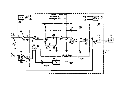
Figure 1 is an electrical schematic diagram of a
preferred form of an energy consumption metering circuit 10
in accordance with the invention for measuring the energy
consumption (in watthours, for example) in a load connected
to an AC power distribution system (not illustrated). As
will be described in more detail shortly, circuit 10 may be
fabricated in integrated circuit form, preferably on a
single monolithic MOS semiconductor integrated circuit
chip 12. The load voltage V1 and the load current I1 in the
electrical system may be sensed by conventional means, and
corresponding voltages VX and vy which are proportional to
the load voltage and load current, respectively, may be
supplied to corre~ponding input circuits 14 and 16 of
circuit 10. Voltage VX may be derived, for example, from
the secondary of a voltage transformer (not illustrated)
which is connected across the voltage lines of one phase of
; the electrical system and may be equal to V1/kV where kv i8
a proportionality constant. Voltage vy may comprise the
; voltage developed across a sensing resistor R due to a
current I1/ki flowing through the resistor from a current
tran#former (not lllustrated) which monitor~ the load
current, where k~ i8 a proportionality constant. Input
circuit 14 may comprise a line for supplying the voltage Vx
to a first terminal of an analog switch S1, and an inverter
amplifier 18 or inverting the voltage and supplying a
voltage ~VX to a second terminal of the switch. Similarly,
input circuit 16 may supply the voltage vy to a first
terminal of another analog switch S2, and include another
inverter amplifier 20 for supplying an inverted voltage -vy
to a second terminal of switch S2. A~ will be described in
more detail shortly, circuit 10 may further compri~e a time
division multiplier (TDM) 22 for multiplying the voltages VX
and vy (or inverted forms thereof) together to form a
voltage vz at the output of switch S2 which correspond~ to
the product of the two input voltages. Since the two input
- voltages VX and vy are proportional, respectively, to the
-6-
12834Sl RD-17,142
instantaneous load voltage and load current, their product,
Vz, i 8 proportional to the instantaneous power being sup-
plied by the electrical system. The signal vz may be then
integrated to convert it into a signal proportional to
average energy and quantized into a train of signal pulses,
each pulse of which represents a predetermined amount of
energy, in an analog-to-pulse rate converter 24. The
voltage va from the analog-to-pulse rate converter may be
supplied to a divider 26, such as a binary divider, which
divideæ the pulse train by a factor N. The pulses from the
divider may be accumulated or counted and displayed in a
register/display (RD) 27 to provide an indication of energy
consumption.
Time division multiplier 22 may comprise a triangular
waveform sampling frequency genera~or (TG) 28, which will be
described in more detail in connection with Figure 2, a
comparator (C0) 30, and switch 52. The comparator receives
at a first input either the voltage +VX or the voltage ~VX
from switch Sl, and receives at a second input a triangular
waveform voltage VT having a frequency f8 from the sampling
frequency generator 28. Comparator 30 constitute~ a pulse-
width modulator which provides pulse-width modulated pulses,
wherèin tho instantaneouQ pulse width of an output pulse is
proportional to the corresponding instantaneous magnitude of
the input voltage from switch Sl. The pulse width modulated
output of the comparator is employed for controlling the
poæition of switch S2 so that the output voltage vz from the
switch comprise~ a train of pulses which alternate in
polarity wherein the instantaneous magnitude of any given
pulse is proportional to the line current while the instan-
taneous width or mark-space ratio of the pulses is propor-
tional to the line voltage. Thus vz is proportional to the
instantaneous power, as explained, for example, in the
afore-referenced Patent No. 3,955,138. The output product,
vz, from time division multiplier 22 is preferably provided
about 100 times for each period of the line frequency.
lZ83~S1
RD-17,142
Accordingly, for a 60 Hz line frequency, the sampling
frequency fs provided by sampling frequency generator 28 is
preferably of the order of 6 KHz.
In analog-to-pulse rate converter 24, the product
signal vz is preferably integrated in a switched-capacitor
integrator comprising an operational amplifier (OA) 32, a
feedback capacitor Cl, an input capacitor C2, and analog
switches S3, S4, S5, and S6. The switches may be controlled
in pairs (as indicated by the dotted lines) by clock sig-
nals l~ 2 which are derived from a clock generator(CLK) 34. The clock signals are non-overlapped and 180
degrees out of phase. The frequency fCl of the clock
signals is preferably high in relation to the frequency fs
of sampling frequency generator 28, and may be, for example,
of the order of 30 K~z. As shown in the figure, switches S3
and S4 are operated together and alternately with
switches S5 and S6 to connect capacitor C2 alternately to
the output of switch S2 an~ to the non-inverting (-) input
of operational amplifier 32, and to ground. Switches S3-S6,
in combination with capacitor C2, effectively constitute a
sampling circuit which samples the signal vz and supplies
the sampled signal to the operational amplifier. This
signal is integrated up in C1. Thus the output voltage VC
o operational amplifier 32 is a ramp signal with a constant
slope formed by superimposed small steps due to sample
integration. In addition, a 2wt component is superimposed
upon the ramp signal due to the effect of multiplication of
the input voltages. This component, however, is cancelled
out in balanced polyphase loads. The output signal VC from
the integrator is thus the time integral of the input
voltage vz with a time constant of (Cl/C2) TCl, where
TCl = l/fcl, and VC represents the average energy being
consumed in the electrical system.
Signal VC from the integrator may be quantized and
converted into a train of signal pulses by a hysteresis
comparator (HCO) 40 wherein each output pulse represents a
lZB3~1 RD-17,142
predetermined quantity of energy. As described, for
example, in the afore-referenced Patent No. 3,955,138, the
hysterosis comparator may comprise a pair of comparators
connected in parallel, each receiving at one input thereof
the output voltage from the integrator. One of the compara-
tors may receive at another input thereof a reference
voltage +VR and provide an output to the set input of a
flip-flop. The second comparator may receive another
reference voltage -VR and provide an output to the reset
input of the flip-flop. During a first time period, Tu, the
integrator may integrate the signal vz upwardly so that the
output ramp voltage VC from the integrator increases. When
this voltage reaches the positive reference voltage, the
flip-flop may be set so that the hysteresis comparator
output may go high to produce an output pulse. This pulse
may be supplied back to switch S1 to control the switch so
as to reverse the polarity of the input voltage VX to
comparator 30 of the time division multiplier. This
reverses the polarity of the product signal vz so tnat the
integrator starts to integrate downwardly during a next time
period Td. Upon the output signal from the integrator
reaching the negative reference voltage, the hysteresis
comparator changes Qtate by going low, which again rever~es
tho input voltage to comparator 30 so that the integrator
starts to integrate upwardly again. The hysteresis compara-
tor output va is thus a pulse train where each pulse repre-
sents a predetermined amount of energy measured, for
example, in watthours. The energy per output pulse is
Wq = (4VR/kfcl) (Cl/C2) (Joules) (1)
and the output pulse rate is
1/Tq = (kfC1/4VR) (C2/C1) VI cos ~ (1/sec) (2)
~2834S~
RD-17,142
where k is a dimensional constant in ohms, VI cos ~ is the
power in the load, VR is a reference voltage, and fCl is the
clock frequency.
From Equation (1), it can be seen that the energy per
output pulqe depends only on the clock frequency fCl, on VR,
and on the ratio Cl/C2. Thus, the accuracy with which the
energy may be measured depends upon the accuracy of these
terms. The clock frequency may be derived from the line
frequency of the electrical system, as by using conventional
phase lock loop techniques, and since the line frequency of
AC power distribution systems is, on the average, stable to
within +0.1%, the clock frequency would have the same
accuracy. The reference voltage VR may be derived from a
voltage regulator (REG) 44 fabricated directly on chip 12,
and the voltage regulator may be formed to be quite accurate
using conventional techniques. As to the capacitor ratio,it
is relatively easy to match the temperature and voltage
coefficients of capacitors formed on a single silicon chip
so that these coefficients track each other over a rela-
tively wide range of temperature and voltage. Thus it ispossible to obtain a desired ratio of the capacitors accu-
rate to within +0.1%, even though the absolute values of the
capacitors may vary substantially from target values.
Assuming that dividor 26 is not included on the output
of the hysterosis comparator and that the output pulses are
supplied directly to the register/display RD, it is conveni-
ent to select Tq = 1 sec. This may be accomplished by
appropriate selection of the ratio Cl/C2. However, thi~
leads to certain difficulties, as will now be explained.
As noted above, it is desirable that the clock fre-
quency fCl be much larger than the sampling frequency fs in
order to obtain adequate information over one sampling
period of vz. An additional requirement on the switched-
capacitor integrator for good linearity is
2Ao (Cl/C2) (l/fcl) >> Tq/2 (3)
--10--
lza34~
RD-17,142
where Ao is the open loop gain of the operational ampli-
fier 32, and Tg/2 is the up (or down) integration time equal
to one-half of the period of the output pulses from the
hysteresis comparator 40. From Equation (3), for a 0.1~
integration non-linearity, the capacitor ratio most be about
C1/C2 = 10 (Tq/2) (fCl/2Ao) (4)
Thus, for an open loop gain Ao = 10 , an output pulse
period Tq = 1 sec, and a clock freguency fCl = 30 KHz, the
ratio C1/C2 is of the order of 750. Thus, Cl must be much
larger than C2, i.e., have a value 750 times that of C2, to
give the reguired ratio. This ratio is prohibitively large
for integration on a silicon chip to afford a reasonable
chip size and to permit good matching between the capaci-
tors. The larger the value of the capacitor, the larger the
; 15 chip area necessary for its fabrication. When the capaci-
tance ratio is large, matching becomes difficult because it
is hard to maintain a desired ratio on a production basis.
With small capacitances, e.g., 0.1 pf, fringe effects may be
guite large in rolation to those associated with larger
value capacitors, e.g., 75 pf. This makes it difficult to
control the value of the ~mall capacitor, and the capaci-
tance ratio may change greatly. When the values of the
capacitor are approximately the same order of magnitude,
much closer matching between the capacitors and much better
integration accuracy are possible. Thus, it is desirable to
reduce the capacitance ratio.
The capacitance ratio may be reduced considerably by
employing divider 26 at the output of hysteresis compara-
tor 40 for dividing the output pulses from the hysteresi~
comparator by a factor of N. In order to maintain the same
energy per output pulse and the same pulse rate as given by
equations (1) and (2) to the register/display, the input
pulse rate to the divider must be increased by the same
': ' ~ ' ~
lZ834~1 RD-17,142
factor N as the division ratio. This requires that the
speed of the integrator be increased by the divider factor N
and the capacitor ratio be reduced by the same factor.
Increasing the integration speed by a factor of N causes the
period of the output pulse train from the hysteresis compa-
rator to decrease to Tq/N, and Equation (4) becomes
Cl/C2 = 103(Tq/2N) (fCl/2Ao) (5)
For the same values of open loop gain, Tq, and fCl as
~ before, selecting the divider ratio~ N = 100 gives a capaci-
tor ratio Cl/C2 = 7.5, which is a reasonable value for
integration on a silicon chip and which permits very close
matching of the capacitors and close control over the
accuracy of the ratio.
Increasing the integration speed by using a divider is
of particular interest in the case of balanced polyphase
watthour metering where the 2~t components are nearly
cancelled. In the case of a single phase meter, these
components are preferably removed before the fast integra-
tion takes place. This may be accomplished by employing a
low pass filter on the input of the switched-capacitor
integrator.
The circuit of Figure 1 affords automatic offset error
correction of system offset voltages. This is accomplished
since during the up-integration period Tu of the signal vz,
system error voltages are integrated up, causing a time
error of +Te~ However, when the integrator output voltage
reaches the reference voltage level and hysteresis compara-
tor 40 output voltage changes state, the input voltage VX to
comparator 30 reverses polarity, as previously described,
which causes polarity of the product signal vz to reverse so
that the integrator integrates down during the down-
integration interval Td. Although the input signal vz to
the integrator reverses polarity, the system offset error
voltage does not and causes a time error of ~Te. Therefore,
-12-
~Z8~45I
RD-17,142
during the total period Tu + Td, the offset time errors are
subtracted and are thus automatically eliminated.
The circuit of Figure 1 has been described in connec-
tion with metering energy consumption in a single phase
electrical system. In order to meter energy consumption in
a polyphase system, it is merely necessary to include, for
each additional phase, input circuits such as 14 and 16 for
receiving voltages proportional to the load voltage and load
current in that phase, a time division multiplier such as 22
for multiplying the voltages together to form a product
signal vz for the phase, and to provide a switched capacitor
input network such as C2 and switches S3-S6. The switched
capacitor outputs, i.e., switch S4 output, from each of the
other phases may simply be connected together and supplied
to the summing point (SP) of integrator operational ampli-
fier 32, as shown in dotted lines in Figure 1. This effec-
tively adds together the product signals vz representative
of the instantaneous power in each of the other phases and
supplies the composite signal to the input of operational
amplifier 32 for integration. The resulting output sig-
nal VC from the integrator then represents average power in
the polypha~e system, and the output pulses to the register
and display 27 indicate the total energy consumption in the
polypha8e system. For metering polyphase power, it is not
necessary that the time division multiplier of each phase
include a separate triangular waveform sampling frequency
generator 28. The same sampling freguency VT from genera-
tor 28 of Figure 1 may be supplied in parallel to each of
the comparators in the time division multipliers of the
other phases corresponding to comparator 30. In addition,
the output from hysteresis comparator 40 may be supplied in
parallel to switches corresponding to switch Sl in each of
the other phases, so that the polarities of the input
voltages VX are all reversed simultaneously. These addi-
tional circuits required for polyphase monitoring may all beincluded on integrated circuit chip 12.
-13-
lZ834S~
~D-17,142
Figure 2 illustrates a preferred form of triangular
waveorm samp1ing generator 28. Other forms of the sampling
frequency generator which may be employed are disclosed in
the afore-referenced patents. However, the generators
disclosed in these patents all employ RC integrators and are
accompanied by the attendant disadvantages previously noted
with respect to fabricating resistors on a semiconductor
chip. The sampling frequency generator of Eigure 2 is
advantageous in that it employs a switched-capacitor inte-
grator, instead of an RC integrator, and it may be moreeasily fabricated on chip 12.
In Figure 2, the switched-capacitor integrator of the
sampling frequency generator comprises an operational
amplifier 50 having a feedback capacitor C3 connected
between its output and its non-inverting input, and a
switched input capacitor C4 controlled by switches S7, S8,
S9, and S10. As with the switched-capacitor integrator of
Figure 1, the switches may be controlled in pairs by non-
overlapping clock phases o3 and 04, which are 180 degrees
out of phase. The clock phases may be derived from a
non-critical clock oscillator 52 and may have a fre-
quency fc2 which is large in relation to the sampling
frequency f5 for example, 60 KHz. Oscillator 52 may be a
separate oscillator similar to clock 34, for example, or
alternatively clock 34 may be formed to provide clock
signals at both frequencies Cl and fc2.
The output of operational amplifier 50 may be coupled
to one input of a comparator 54, the other input of which
receives one of the reference voltages IVr or -VR in accor-
dance with the closure of one of switches S11 and S12. The
output signal of comparator 54 may be employed for control-
ling switch S12 and for controlling another switch S13, as
shown, and may be supplied to an inverter amplifier 56, the
output signal of which controls switch S11 and another
switch S14. Switches S13 and S14 connect the reference
-14-
~Z 8 3 ~ ~1 RD-17,142
voltages ~Vr and +Vr, respectively, to the input of
switched-capacitor C4.
The sampling frequency generator of Figure 2 functions
in a manner similar to that previously described for the
switched-capacitor integrator of Figure 1. The integrator
integrates one of the reference voltages (depending upon
which of switches S13 and S14 is closed) to provide either
an increasing or a decreasing triangularly-shaped ramp
voltage VT, as indicated by the waveform alongside the
output lead from operational amplifier 50, which varies
between the reference voltages with a time constant of
+ (C3/C4) (1/fc2). When the output voltage from the inte-
grator reaches either the positive or the negative value of
the reference voltage, the output signal of comparator 54
changes state causing switches Sll-S14 to be operated, which
reverses polarity of the integrator input voltage so that
the integrator begins to integrate in the opposite direc-
tion.
All of the various components illustrated within the
dotted line 12 of Figure 1 and in Figure 2 may be readily
implemented in a well-known manner in integrated circuit
form. The various analog switches Sl-S14, for example, may
be implemented as conventional CM05 switche~. Since the
entire energy consumption metering circuit may be fabricated
on a single integrated circuit chip, it may have a small
size and may be produced rather inexpensively. The use of
switched-capacitor integrators is particularly advantageous
since, as indicated above, the ratios, voltage coefficients,
and temperature coefficients of the capacitors may be well
matched over a relatively wide temperature and voltage
range. In fact, the temperature and voltage coefficients of
integrated circuit capacitors are generally smaller than
those of discrete components, and since the coefficients of
integrated circuit capacitors can be matched quite well,
fabrication of the metering circuit in integrated circuit
form affords high accuracy metering of energy consumption.
~Z83451 RD-17,142
Also significant is the use of a divider, such as 26, at the
output of the hysteresis comparator of the analog-to-pulse
rate converter, since it enables the capacitor ratio of the
switched-capacitor integrator to be reduced, thereby
reducing the chip area required for fabricating the capaci-
tors, improving the capacitor ratio matching, and affording
a higher integration speed.
While a preferred embodiment of the invention has been
shown and described, it will be appreciated by those skilled
in the art that changes may be made in this embodiment
without departing from the principles and spirit of the
invention, the scope of which is defined in the appended
claims.
-16-