Note: Descriptions are shown in the official language in which they were submitted.
1;~8347~
Field of the Invention
The invention relates to circuits used to accurately read
data pulses transmitted from storage media, such as floppy
disks, despite the presence of frequency errors and phase errors
during reading of the data. The present invention can operate
to interface a disk drive subsystem with a host computer
system. This invention further relates to digital phase locked
loop circuitry that can be used to interface floppy disk storage
media with personal computers.
Background of the Invention
Digital computers transfer information in the form of
digital pulses to and from a resource memory to which the host
computer system has access, whether the memory is located within
the system (local) or at a remote location. In processing the
data, it is necessary that the timing of these pulses be
determined and controlled so that the various logic functions
occurring in the host system can be synchronized with the
transfer of digital pulses representing digital data contained
within the resource memory.
Information, including program instructions as well as
other data, is typically stored in a resource memory on a
magnetic medium, and each bit of digital data typically appears
as a magnetic transition area on the surface of the medium. In
order for the host computer to have access to such data, it is
important that the bits of data be accurately positioned on the
magnetic medium and be capable of being accurately read
therefrom. With the growth in the market for personal
computers, the use of a particular type of magnetic memory
--1--
~k
~ Z83479
device, the floppy disk, has greatly increased. Furthermore, as
personal computers have been redesigned for greater memory
capacity and speed, the storage capacity of floppy disk used
with these computers has been increased by increasing the
density of the digital data recorded on the floppy disk.
The use of disks as storage media is accompanied by certain
problems, however, particularly for disk drive systems used in
host computer systems available in the less expensive personal
computer and business word processor markets. Although it is a
design criteria of disk drive manufacturers to accurately
control the speed of rotation of the disk in order to have a
fixed period of disk rotation and thereby maintain a
predetermined frequency at which one can read data from the
disk, one problem is frequency drift during data transfers due
to unsteadiness in motor drive speed. This results in frequency
error and can cause the data on the disk to be read
incorrectly. Another problem is migration of the magnetic
transition areas, and thus the data bits on the storage medium,
due to the inherent characteristics of the magnetic disk. This
results in phase error during data transfers and can also result
in incorrect data reads. These sources of error are present in
every disk drive system to a certain extent, and are addressed
by the circuitry of the present invention.
Summary of the Invention
An object of the present invention is to provide a data
input circuit for a host computer system that has access to a
resource memory, such as a floppy disk. The circuit is capable
of processing data pulses received from a disk drive and adjusts
--2--
3347~
the input circuit to compensate for phase errors and for
frequency errors while the data is being read. Phase locked
loop circuitry is implemented to establish inspection windows
that can be varied in time duration and/or time of start and
stop of the windows. The windows are adjusted so that each
subsequent data pulse from memory will occur in the middle of an
inspection window.
The input circuit processes each received data pulse to
determine if there is a phase error, i.e., the data pulse has
shifted from its expected time of arrival, or a frequency error,
i.e., the data pulses are arriving at an increased or decreased
frequency rate and therefore are not received at the expected
time. Frequency measurement and correction, and phase
measurement and correction, are carried out by two separate
dedicated portions of the circuit.
The circuitry of the invention keeps track of the times of
arrival of prior data pulses in order to measure and correct for
frequency and phase drift of the data pulses being read from the
disk. An up-down counter and an adder are included in the phase
locked loop to digitally indicate the precise time of arrival of
the data pulses from memory. Decoder circuits process the
digital arrival time information for a data pulse or pulses and
generate correction signals that are fed back to the counter and
adder circuits. The correction signals adjust the duration and
start/stop time of each inspection window by causing the
duration and/or start/stop time for one complete cycle of the
adder to vary. After each complete adder cycle, a carry signal
334~9
is sent to a buffer. If a data pulse was received at any time
during that one adder cycle (chich corresponds to an inspection
window), a ~1" will be input and stored. Thus, the buffer will
temporarily store data bits that match the data contained in the resource memory being transmitted to the input circuit.
Brief Description of the Drawings
The present invention will be better understood from a
reading of the following detailed description of the preferred
embodiment in conjunction with the accompanying drawings, in
which:
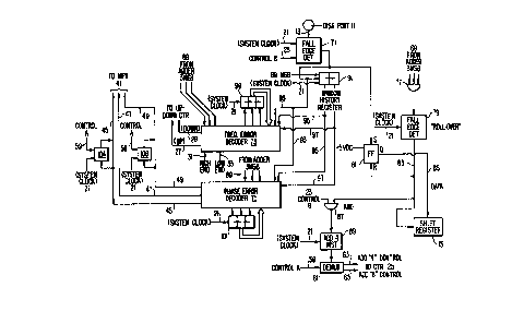
Fig. 1 is a block diagram of the data input circuit of the
invention and
Fig. 2 is a block diagram of the control circuit used in
the data input circuit of Fig. 1.
Detailed Description of Preferred Embodiment
A data input circuit is implemented using NMOS LSI digital
circuitry and operates to process data pulses received from a
resource memory, including data formatted by and received from a
floppy disk. The input circuit can process bits of data in
typical formats arriving at 4, 6, 8 or 12 microsecond intervals,
which enables it to be used with a number of commercially availa-
ble personal computers. The data input circuit ensures that the
data pulses are converted into data bits and stored in the shift
register 15, or input data buffer, as a sequence of bits that
correctly reflects the data bits stored in the resource memory.
Data is received in the form of pulses and is binary (ones or
zeros), with the specific absence of a pulse interpreted by the
1~83479
circuitry as a zero. An error occurs if a shift in the time
of arrival of a pulse creates an error in the ordering of the
data bits as interpreted by the host computer system, so that
the data bits input into the input data buffer 15 and
processed in the host computer system do not match the data
bits stored in the resource memory. The input circuit detects
data pulses transmitted from the resource memory and processes
them as data bits in an ordered sequence. A "one" is input
into register 15 if a pulse is received at any time during a
particular receive (adder) cycle; otherwise a "zero" will be
stored in the register as the value of the current data bit.
The period of the receive (adder) cycle is chosen to
conform with the expected data transfer rate of the memory.
Ideally, individual pulses will each be received in the middle
of one of a sequence of these receive cycles. Each receive
cycle immediately follows the preceding cycle and the time
period from beginning to end of the cycle can be referred to
as an inspection window. The input circuitry receives a bit
stream from the resource memory containing a series of ones
and zeros and detects each successive data pulse during one of
a series of these inspection windows. Inspection windows
have durations and start/stop times that are a function of the
basic data bit transfer rate and the deviation in the times of
arrival of the most recently detected data pulses from the
ideal. Thus, if, for example, there is a basic phase shift of
several nanoseconds in the times of arrival of the immediately
preceding data pulses from the resource memory, this is
compensated for in the data input circuitry by adjusting the
lZ~3347~
start/stop times of the receive cycles. If there is a
frequency shift affecting data transfers so that the period
between the immediately preceding data pulses is gradually
expanding or shortening, this is also compensated for in the
data input circuitry by adjusting the duration of the receive
cycles. After a receive cycle has ended, a carry signal is
generated by the data input circuitry. This carry signal marks
the end of an inspection window and causes a "one" to be
clocked into the shift register 15, or data input buffer, if a
data pulse was received at any time during the window, and
causes a "zero" to be stored in the buffer if no pulse was
received.
The input circuit in Figure 1 is connected to a storage
medium, such as a floppy disk drive, through a disk port 11.
Bits of data are transferred in serial form, one at a time, on
a line 13 from the disk port 11, through circuits shown in
Figure 2, and finally to a buffer, the shift register 15. This
shift register 15 is clocked by the carry signal on line 17
generated by a control circuit 19, whereby data is input and
stored in the register 15, and can then be converted from
serial to parallel form and transferred to other processing
circuitry in the host computer system.
The data line 13 is also input to the control circuit 19.
System clock pulses on lines 21, available in the host computer
system or from a dedicated oscillator made a part of the present
circuitry, control the timimg of the data input circuit and syn-
chronize its operation with the circuitry of the host computer
system. In a typical system, data pulses may be one-half to one
~~~ -6-
9~' '`;C,
1~3479
5 crosecond wide with a 4, 6, 8 or 12 microsecond period between
pulses. A "one" is indicated by a low level--a pulse with a
leading edge going low and a trailing edge returning to high.
The system clock pulses on lines 21 are generated at a suitable
frequency, such as 7.16 MHz. The basic clock rate of 7.16 MHz
was chosen to be 28 times faster than the fastest expected rate
of arrival of data pulses from the resource memory (i.e., 4
microseconds) and 14 times faster than the receive (adder) cycle
rate used to generate the typical inspection window.
An 8 bit up-down counter 25 receives system clock pulses on
line 21, an increment up instruction on line 27, an increment
down instruction on line 29, an add 4 instruction on line 63,
and an add 8 instruction on line 65. The counter 25 has three
8-bit parallel outputs: On lines 35 a-h, 37 a-h, and 39 a-h. A
multiplexer 41 operates as a selection switch to pass only the
value on either the output lines 35, output lines 37, or output
lines 39 as an input to an adder circuit 43 from the counter.
The adder 43 is a serial adder, and can be switched to operate
as either an 11 or 12-bit adder, so that the input circuit can
20 operate in two different speed modes. Adder 43 is clocked in
operation by the system clock. Each sum result at the adder
output is input via lines 67 into the adder 43 again so that
during each adder cycle the adder continually adds the value of
the prior sum result at its output to the value of one of three
25 possible counter outputs selected by the multiplexer 41. The
three most significant bits of the sum result output of the
adder 43 are input to the control circuit 19 via lines 69.
~;~83479
The variable output at lines 37 of counter 25 is initially
set to a nominal value of 146. ~hen the adder is in the ll-bit
mode, the adder can output a sum result as high as 11111111111,
or 2047 in decimal. A nominal center value of 146 was chosen as
the variable output at lines 37 of the up-down counter to the
adder as an approximation of 2048 divided by 14. As a result,
there are approximately 14 clock pulses for each complete cycle
of the adder (i.e., receive cycle), so that the ll-bit adder 43
in ideal operation (no phase or frequency errors) will add the
number 146 that is input via lines 37 to its previous total on
each clock pulse and will therefore "roll over" back to the same
result (because the total number of counts of 2048 is not evenly
divisible by 14, however, the count will be four less than the
count 14 clock cycles before) after 14 clock pulses. The
counter 25 variable output at 37 can be increased using the
increment up signal at 27 up to a maximum value of 159, at which
point any higher increase is inhibited and a high end stop
signal at line 31 is output from the counter 25 to the control
circuit 19. Likewise, the counter 25 can be decreased using the
increment down signal at 29 but will not decrease below a value
of 134, at which point the counter 25 provides a low end stop
signal at line 33 to the control circuit 19. If for some reason
the counter variable output is out of range, the control circuit
19 will respond to the stop signal by sending out either
increment up or down signals until the variable output is back
within the limits.
A hardwired value of 258 is a fixed high output 35 a-h from
the counter 25, and a hard~ired value of 34 is a fixed low output
33479
39 a-h from the counter 25. The counter output 37 a-h is the
variable output and can range in value from 146 to any number
counted up or down therefrom, as constrained by the upper and
lower limits of 159 and 134 set on the counter 25. Three
control lines 45, 47, and 49 are output from the control circuit
19 to the multiplexer 41 and control the selection of one of the
three counter outputs: the fixed low output 35, the variable
counter output 37, or the fixed high output 39.
The host computer system provides the system clock pulses
on lines 21, a control A signal on lines 59, and a control B
signal on lines 23. The state of the control A signal indicates
whether the resource memory utilizes single density or double
density disks. Adder 43 is placed in one of two modes by a
switch 51, which is connected to adder 43 and receives an output
from the adder at line 53. The control A signal on line 59 sets
the state of switch 51. If the adder is set in the 12-bit
state, the output data is reinserted to the adder 43 via line 57
without any jumping or skipping of a bit. If the switch 51 is
set for the ll-bit state by the control A signal, this causes
the adder via line 55 to bypass one of the stages of the adder
and to skip a bit when counting. The adder 43 cycles around
twice as fast when it is operating in the ll-bit state so that
the inspection windows (and receive cycles) associated with
the input circuitry when in this mode have one-half the period
of those when the adder is in the 12-bit state. The inspection
windows have nominal durations of two microseconds for the
ll-bit adder and 4 microseconds for the 12-bit adder.
_g_
3475'
The control circuit 19 is implemented as shown in Figure 2.
Data pulses on line 13 from the disk port 11 are input to a
first falling edge detector 71, or input data bit detector,
which detector 71 provides a pulse output after detecting the
falling leading edge of a data pulse representing a "one~ from
the resource memory received on line 13. The first detector
pulse output is generated in synch with the system clock on line
21, which clocks the output of detector 71. The state of the
control B signal indicates whether the host computer system is
in a read mode or write mode of operation. The control B signal
on line 23 is input into the data bit detector 71 to selectively
disable operation of the detector when the host computer system
is in the write mode because the host computer system does not
read or process data from the resource memory in this state.
The three most significant bits of the adder sum result on
lines 69 of the adder 43 are input into a first AND gate 77.
The output of this first AND gate 77 is input to a second
falling edge detector 79. This second detector 79 is also
clocked by the system clock to synchronize its output pulses,
which are generated after the falling edge of an output from AND
gate 77, with the host system. The second detector 79 and first
AND gate 77, or means for detecting the end of a receive cycle,
detect when the output of the adder 43 completes an adder cycle
and rolls over. This occurs when the calculated sum result that
would be output by the adder if it had additional bits exceeds
its actual capacity, so that the three most significant bits on
lines 69, which were all high, switch to the zero state,
whereupon the first AND gate 77 output goes low and second
--10--
,
1283479
detector 79 outputs a pulse. A D (data) flip flop 81, or input
data bit latch, has the output of the first detector 71
connected to its set terminal and the output on line 83 from the
second detector 79 connected to its reset terminal. Thus, if a
data pulse is detected during a receive cycle, a "one" will be
store in the flip flop. At the end of the receive cycle, the
latch will be reset to zero by second detector 79. The Q output
on line 85 of the flip flop 81 is input to shift register 15,
and is used to serially input bits of data from the memory one
at a time per adder (receive) cycle to the shift register 15.
The output line 83 of the second detector 79 is input to the
shift register 15 as a clocking signal, and is the carry signal
on line 17 of Figure 1 used at the end of an inspection window
to cause whatever data bit was stored in the latch 81 during the
window to be input as the next bit of data stored in the buffer
15.
The output from the first detector 71 is also input as a
clock or enable signal to a shift register 91. The shift
register 91 stores a lag/lead history bit for each pulse and
shifts the stored data in response to the detection of any
additional pulses. The 11 or 12-bit output of the adder 43
indicates the time of arrival of a data pulse in relation to the
beginning of the adder (receive) cycle. If it is desired to
keep data pulses in, for example, the middle of the inspection
window and receive cycle, and the adder cycle is defined as
beginning at zero, then the lag or lead status of a received
pulse is easily determined by input of only the most significant
bit of the adder 43 on lines 69 to register 91. Thus, the
--11--
347~
register 91 stores the value of the most significant bit of the
adder output when each of the two previous data pulses were
detected. A "one" indicates the data pulse was detected
sometime after the center of the inspection window passed (lag),
and a "zero" indicates the data pulse led the center of the
inspection window and adder cycle. The shifting of the register
91 causes the retention of the lag/lead history of only the to
preceding data pulses detected at the first detector 71.
The output from the data pulse detector 71 is input via
line 93 and the two bits of lag/lead history are likewise input
via lines 95 and 97 into a frequency error decoder 73 and a
phase error decoder 75. The first decoder 73 corrects for
frequency drift and the second decoder 75 corrects for phase
drift as data pulses are being transmitted from the resource
memorY-
To determine if an error has occurred, each decoder looksat a history of several pulses, e.g., the current data pulse,
and the preceding two data pulses from shift register 91. A
3-bit frequency error parallel/serial shift register 99, or
correction amount register, clocked by system clock pulses
receives in parallel form three bits from the frequency error
decoder 73 that indicate whether additional frequency
corrections are required during subsequent clock cycles.
Register 99 acts as storage for additional correction commands
to be read serially back into the frequency error decoder 73
during successive clock cycles. A 3-bit phase error
parallel/serial shift register 101, or correction amount
register, clocked by system clock pulses receives in
-12-
- 1~83479
parallel form three bits from the phase error decoder 7S that
indicate whether additional phase corrections are required during
subsequent clock cycles. Register 101 acts as storage for
additional phase correction commands to be read serially back
into the phase error decoder. The three most significant bits
of the sum result of adder 43 on lines 69 form additional inputs
to the frequency error decoder 73 and the phase error decoder 75.
The freguency error decoder 73 can provide an increment up
signal at 27 or increment down signal at 29 to the up-down
counter 25 to direct the counter to increase or dcrease the
count of its variable output 37 by one (initial nominal value is
146). The period of the adder ~receive) cycle can thereby be
increased or decreased because the adder sum result will roll
over at a different rate when a number other than 146 is added
every clock cycle. The high end stop signal 31 and the low end
stop signal 33 from the up-down counter 25 are also input into
the frequency error decoder 73. The phase error decoder 75
provides either a select low count signal on line 45, a select
variable count signal on line 47, or a select high count signal
on line 49 to the multiplexer 41, which selects one of counter
outputs 35, 37 or 39, respectively, to be input to adder 43 in
response. As a result, the sum result in the adder 43 during
the next clock cycle is either increased by a count o 34, a
count of 258, or a variable count between 134 and 159.
The up-down counter 25, multiplexeer 41, and adder 43 define
the duration and start/stop time of the inspection window, during
which any detected data pulse from resource memory will be read
-13-
3479
as the next data bit into buffer 15. If detected data pulses do
not occur at a regular predetermined time, e.g., the middle, in
relation to the start and stop times of the inspection window,
there is a phase error. If data pulses are received at a rate
deviating from the expected period of either 4, 6, 8 or 12
microseconds, there is a frequency error. During each cycle,
the logic in the frequency error decoder and phase error decoder
is used to adjust window duration and start/stop time to center
the window around the last data pulses received.
The circuitry establishes a nominal variable output of 146
for counter 25 to set a nominal window size for the inspection
window, which results in the use of two microsecond wide windows
when the control A signal selects an ll-bit adder mode. With
this algorithm, data pulses received every 4 microseconds appear
in every other window, 6 microsecond data appears in every third
window, and 8 microsecond data appears in every fourth window.
Window size is adjusted to accommodate for deviations in the
frequency of data transfers from memory by increasing or
decreasing the variable output of the up-down counter to the
adder 43. For example, the data transfer rate may be slower
than the nominal rate and therefore, data pulses would be
detected after the center of the inspection window. Each adder
~receive) cycle, the data pulses would be detected as lagging
the center of the window, and as a result, the most significant
bit of the sum result for the adder 43 would be a "one~ at the
instant during the adder cycle that a data pulse is detected.
Accordingly, the shift register 91 would be filled with a string
of ~ones~ to indicate the lag/lead history for preceding pulses.
-14-
1;~83479
The decision to make a frequency correction is made in the
frequency error decoder and results when the lag/lead history
bit for the preceding pulses, as well as the most significant
bit of the sum result for the adder for the current data pulse,
indicate that the most recent data pulses are all falling on one
side of the window. AS a result, an increment down signal on
line 29 is sent from the frequency error decoder to the up-down
counter 25, which decreases the count of the variable output on
lines 37 by one (e.g., from 146 to 145). This decrease in the
size of the variable output of the up-down counter will decrease
the number being added to the sum result during each clock cycle
by the adder 43, and, as a result, the adder 43 will not turn
over as quickly and the period of the adder (receive) cycle will
increase. Thus, the duration of the inspection window will be
increased to account for the slower rate at which data pulses
are being detected from the resource memory. A similar process
occurs if the data transfer rate from the resource memory begins
to increase (so that data pulses are consistently leading the
center of the inspection window), requiring an increase in the
count of the variable output on lines 37.
Phase corrections are made by the phase error decoder,
which will output a select low count signal at 45 or select high
count signal at 49 to the multiplexer 41 when a phase error
exists. Thus, instead of adding a value between 134 and 159 to
the sum result of the adder 43, a value of 258 or 34 will be
selected by the multiplexer 41 among the outputs from the
counter 25 during several (up to four) of the subsequent clock
~ ;~834'7~
cycles and added to the sum result by the adder 43. The phase
error decoder decides whether to output the select low count
signal 45 or the select high count signal 49 based on the value
of the most significant bit of the sum result being output by
the adder 43 on lines 69. For example, if the last data pulse
lagged the center of the adder (receive) cycle, a select low
count signal at 45 can cause the sum result of the adder to roll
over only after 15 (instead of 14) clock cycles and would
therefore delay by a fixed amount the start/stop times of
subsequent inspection windows.
The extent of the frequency corrections and phase
corrections that are made during each adder cycle, and whether
such corrections should be made at all, depends upon the amount
of the error as reflected by the amount of time by which the
detected data pulse leads or lags the center of the inspection
window. The size of this lag or lead is determinable because
the sum result of the adder that is output on lines 69 indicates
the precise time of arrival of the data pulse with respect to
the beginning of the adder cycle. The three most significant
bits from the adder sum result are input to both the frequency
error decoder and the phase error decoder in order to enable the
logic circuits therein to vary the amount of correction made
during any given adder cycle to the duration and start/stop
times of the inspection windows. For example, a binary value of
100 for the three most significant bits would indicate only a
small lag in the arrival of the latest data pulse, whereas a
value of 000 would indicate an extremely large lead. In the
embodiment shown in the drawings, the size of a frequency or
-16-
1;~8347~
phase correction during any one system clock cycle is fixed and
discrete. However, the relative magnitude of the phase and
frequency corrections made during a complete receive cycle can
be varied by the decoders 73 and 75 by making up to four
corrections by causing the same correction to occur during up to
four distinct system clock cycles. The parallel/serial shift
registers 99 and 101 indicate whether additional corrections for
phase and frequency errors will be made. Either 000, 001, 011,
or 111 is loaded by the decoders 73 and 75 into their respective
correction amount registers 99 and 101, depending on the
magnitude of the three most significant bits of the sum result
from the adder 43. Thus, the bits loaded into the 3-bit shift
register 101 by the phase error decoder would be 000 if the
three most significant bits had binary values of 011 or 100,
bits 001 would be stored in register 101 if the most significant
bits from the adder were 01C or 101, bits 011 would be sent to
register 101 if the most significant bits read 001 or 110, and
bits 111 would be output to register 101 if the most significant
bits read 000 or 111 (which indicates the maximum possible
amount of lead and lag by an input data pulse). The registers
99 and 101 are loaded with the additional correction amount bits
during the same clock cycle that the first frequency and/or
phase correction is being made. On subsequent clock cycles, the
bits stored in the correction amount registers 99 and 101 are
serially shifted one bit at a time into the frequency error
decoder and the phase error decoder. The additional correction
requests input as a bit to the decoders 73 and 75 cause each to
1~347'~
make corrections exactly as described before during additional
clock cycles if the bit serially shifted in from the respective
correction register indicates an additional correction is
needed. Thus, in the preferred embodiment shown in the figures,
the correction amount registers are necessary because a
correction made during any one clock cycle has only a single
fixed magnitude.
The counter 25 and adder 43, in cooperation with the
freqency error decoder 73 and the phase error decoder 75 (which
determine the amount of feedback received by the adder), form a
digital phase locked loop responsive to data pulses received
from the resource memory. The phase locked loop tracks a train
of data pulses from the memory which may vary in phase and in
frequency. The speed at which the sum result of the adder 43
rolls over, which corresponds with the duration and start/stop
times of the receive (adder) cycle (or inspection window), is
continually being adjusted with feedback that matches the phase
and frequency of the receive (adder) cycles with the phase and
frequency of the data pulses received at the data bit detector
71. The phase error decoder adjusts the phase of the adder
cycle (changes the start/stop times of the inspection window) in
order to maintain the data pulses in the center of the
inspection windows. The frequency error decoder adjusts the
frequency of the adder cycle (changes the size of the inspection
window), and thereby adjusts the period of receive cycles so
that they match or are evenly divisible into the period between
successive data pulses. The nominal value of 146 by which the
sum result of the adder is normally incremented was selected in
-18-
1;~8347~
order to have the time it takes to complete one adder (receive~
cycle be divisible into a typical transfer rate of bits from a
floppy disk. A well-designed phase locked loop, used to track a
varying input signal, should be fast settling but stable. A
large amount of phase correction causes the loop to settle
faster, but also makes it more sensitive to noise. On the other
hand, if too much frequency correction is used, the loop can
become unstable. The proper ratio of phase and frequency
correction provided in the loop is important. The amount of
phase correction must hold the next data input pulse in the
correct inspection window while enough frequency correction is
provided to ensure that the inspection windows are of the
correct duration. If not enough phase correction is provided,
it is possible for a data input pulse to be detected during the
wrong inspection window, and this in turn would prevent a proper
determination of the amount of needed frequency correction. The
nominal variable counter output of 146, as well as the fixed low
value of 34 and the fixed high value of 258, are selected in
order to maintain the proper ratio of phase and frequency
correction feedback. Thus, if only a small phase correction is
needed for a lag in the train of input data pulses, the addition
of only 34 (instead of 146) to the sum result of the adder
during one clock cycle will probably cause the adder to take one
extra clock cycle to roll over. A single frequency correction,
incrementing the variable counter output from 146 to 147, will
slow the adder cycle rate by .7~. It has been determined that
smaller percentage changes in the period of the phase locked
loop do not provide much of an improvement in performance,
whereas problems in reading data from floppy disks may become
-19-
1 ~ ~3 ~7~
noticeable if the duration of the inspection windows cannot be
adjusted by a fine enough amount.
When the input circuit is in the 12-bit adder mode, the
cycle period for the adder and the phase locked loop is
S nominally four microseconds, or 28 clock cycles. The inspection
window is twice as long, so that a single frequency correction
from, e.g., 146 to 147, changes the sum result of the adder by a
total of 28 counts rather than 14 counts during each complete
adder cycle. However, a single phase correction from, e.g., 146
to 34, continues to change the adder sum result by a total of
112 during one adder cycle regardless of the adder mode.
Therefore, by changing the nominal cycle time of the phase
locked loop from 2 microseconds to 4 microseconds in switching
to a 12-bit adder, the amount of frequency correction feedback
is effectively doubled when compared with the amount of phase
correction feedback. As described above, a proper ratio of
phase and frequency correction feedback is desirable, and too
much frequency correction can cause oscillation of the phase
locked loop. Therefore, to maintain the same ratio of phase and
frequency correction feedback when switching from the ll-bit to
12-bit adder mode, double the normal phase correction of 112
counts per adder cycle is needed. This is accomplished with the
pulse-doubling one shots 104 and 106. Doubler structures are
connected to select lines 45 and 47, which are output from the
phase error decoder 75 to the multiplexer 41. They cause the
high or low count select signals, if output by the phase error
decoder, to be repeated after four clock cycles so that the
fixed low value of 34 or high value of 258 is output twice
-20-
1~8347~
~s often from counter 25 into adder 43, and thereby provide for
multiplying the amount of phase correction by a factor of two
when the adder 43 is operating in the slower 12-bit mode.
Subsequent corrections requested by the correction amount
register 101 are executed without interference by delaying the
phase correction commands from the doubler structures by four
clock cycles. A first one shot 104 operates as a pulse repeater
connected to line 45. This one shot circuit 104 will receive a
pulse on line 45 output by decoder 75, and then repeat it by
placing a second pulse on the line 45 to multiplexer 41 after
the required delay if the control A signal on line 59 for
selecting 12 bits is input into the one shot circuit 104. A
second one shot circuit 106 is similarly responsive to the
control A signal on line 59, and is connected to control line 49
to act as a pulse repeater with respect to line 49. As a
result, the magnitude of any phase correction is doubled from a
minimum total of 112 counts in the ll-bit mode (146 versus 34 or
258) to a total of 224 counts in the 12-bit mode.
When the host system is in the write mode of operation, the
state of the control B signal on line 23 changes so that data
bits cannot be input from the disk port 11 into the data input
buffer 15. Instead, data bits are written from an output data
buffer (not shown) to the resource memory, and the same carry
signal on line 83 can be used to clock data bits both into the
data buffer 15 and out of the output data buffer during data
transfers with the resource memory. When writing data onto a
1~3475~
- memory device, it is important to keep the period between each
transmitted data bit as stable as possible. In the ll-bit adder
mode, a data bit is output every 14 clock cycles in the write mode
in response to the carry signal. In order to maintain this
S uniform period between carry signals in the write mode, an error
correction is built into the circuitry to operate only in the
write state, gated on the state of the control B signal on line
23. A potential deviation in adder cycle duration exists because
the nominal inspection window width of two microseconds is not
evenly divisible into 14 even time increments when using an adder
that makes a total of 2048 counts. If a correction were not made,
the adder 43 would sometimes complete its count (and cause a carry
signal to clock data out of the output data buffer) in 13 clock
pulses instead of always in 14 pulses. Division by 14 of the
ll-bit adder maximum count of 2048 leaves a remainder of 4.
Therefore, every 14 (ll-bit mode) or 28 (12-bit mode) clock
pulses, the adder sum result must be increased by a fixed amount
so that the identical sum result appears every 14 or 28 clock
pulses. When the control A signal on line 59 for 11 bits is
applied to the circuit, an add 4 command is sent as an instruction
to the counter 25. When the control A signal is set for 12 bits,
an add 8 command is sent to the counter. The add 4 and add 8
commands are generated only once per adder cycle in respone to AND
gate 87 being enabled by detector 79 when the adder 43 rolls over
ZS and begins a new adder cycle. Either the add 4 or add 8 command
is selected by demultiplexer 61 in response to the state
347~
of the control A signal, and the proper command is sent out as a
pulse on line 63 (add 4) or line 65 (add 8). The add 4 and add
8 commands, are synchronized with the system by instruction
generator 89, which receives inputs from AND gate 87 and the
system clock and outputs a signal to the demultiplexer 61.
The combinatorial functions performed by the decoders 73 and
75 are implemented using a programmable logic array (PLA). The
techniques for programming the PLA to implement a truth table
are well known to those skilled in the art. In the ideal
embodiment, the phase decoder 75 does not utilize the inputs
from the history register 91. The relation between the decoder
inputs and outputs is as follows:
1~8347~
TABLE 1
INPUT PHASE CORRECTION OUTPUT
(from MBS of adder) (112/2048 of cycle = +1)
0 +4
23 +2
4 -1
-2
7 -4
,
TABLE II
ERROR HISTORY INPUT
(none in same direction - 0)
MBS INPUT O
FREQUENCY CORRECTION OUTPUT
11/146 = +1)
0 0 +3 +4
1 0 +2 +3
2 0 +1 +2
3 0 0 +1
4 0 0 -1
0 -1 -2
6 0 -2 -3
7 ~ 0 -3 -4
The disclosure~ ~n U.S. patents 4,780,844 issued October 25,
1988 and 4,874,164 show related systems.
The above description of the invention is intended to be
illustrative of a single preferred embodiment. Changes can be
made to the structures described herein without departing from
the features and scope of the invention.
-24-
~ ~`