Note: Descriptions are shown in the official language in which they were submitted.
7()7
P~IN 12.144 1 24.05.1988
"Receiver ~or a phase-shift keyed carrier si~Jnal."
The .invPntion relates tc, a receiver for a passband signal
generated by phase-shift keying ,~ a carrier .Ln accordance with a data
signal of a predetermined ;ymhol rate 1/T, the receive:r comprising:
- demodulation means for demodulating the received passband signal with
the aid of a local carrier and thereby producing a demodulated data
signal;
- regeneration means for regenerating the demodulated data signal with
the aid of a local clock and thereby producing a regenerated data
si.gnal;
- carrier recovery means having a local carrier generator included in a
phase-locked loop and connected to the demodulation means, and having a
remodu].ator for phase-shift keying of the received passband signal in
accordance with the regenerated data signal and thereby producing a
carrier component as an input signal for the phase-locked loop; and
- a local clock generator connected to the regeneration means.
A receiver having such a structure is known from the
second edition of the book "Phase Lock Techniques" by F.M. Gardner,
Wiley, New York, 1979, Chapter 11, Section 11.2, pp. 216-230.
For data transmission with the aid of phase-shift keying
(PSK) of à carrier, a first requirement for an optimum detection of the
data signal is the availability of a stable local carrier with little
phase jitter in the receiver to enable coherent demodulation of the
received modulation band signal (PSK-signal). A known method to obtain
this local carrier utilizes the principle of PSK-remodulating the
received PSK-signal in accordance with the demodulated data signal for
producing a carrier component that is used as an input signal for a
phase-locked loop (PLL) in which a local carrier generator is included
(cf. Figs. 11.4, 11.5 and 11.8 on pp. 219, 220 and 223 of the above-
mentioned book by Cardner). In applications of the receiver in systems
in which the available signal power is limited and the channel
properties are unfavourable, as is the case in systems for satellite
communication and systems for mobile communication, the signal-to-noise
1~37'J7
PHN 12.144 2 24.05.1988
ratio (SNR) at the input of the receiver can as3ume relatively low
values. In the recircumstances, the PSK-remodulation should preferably
be performed by using thedata signalm regenerated as regards amplitude
and instant of occurrence Lnstead of the demodulated data signal itself,
as tl1e improvement in noise suppression has achieved thereby
for its result that a reliable recovery of the carrier can be ensured
at lower SNR-values at the input of the receiver. True enough, the
errc)r probability of the received data symbols becomes indeed greater
at these lower SNR-values, but the influence of the increased error
probability can effectively be combated by the use of error-correcting
(ode3 as long as the receiver has the disposal of a reliably recovered
carrier. A requirement to achieve this improvement in the transmission
quality is that the receiver disposes, also at these lower SNR-values,
of a stable local c].ock with little phase jitter. When to that end use
is made of the known metl1ods for recovering the local clock from the
demodulated data si~nal, as described in Section 11.3, pp. 230-249 of
said book by Cardner, there is however the disadvantage that the
generation of a clock component as an input signal for a phase-locked
loop including tl1e local clock generator, generally requires operations
which result in the introduction of additional noise in the control
signal for the local clock generator. This is more specifically the case
with operations such as rectifying, squaring or limiting, which are
based on the use of elements having a non-linear amplitude transfer
cllaracteristic. The additional noise thus introduced implies that higher
SNR-values are required at the input of the receiver so as to be able to
ensure a reliable clock recovery.
The invention has for its object to provide a novel
concept for obtaining a local clock in a receiver of the type defined in
the opening paragraph, the concept rendering it possible to improve the
reliability of the carrier covery at low SNR-values at the input of the
receiver.
According to the invention, the receiver is therefore
characterized in that
- the regeneration means are arranged for also producing a delayed and
an advanced version of the regenerated data signal with a delay and an
advance, respectively, relative to the regenerated data signal, over a
time interval A less than symbol interval T, and
7()7
PHN 12.144 3 24.05.1988
- the receiver also includes means responsive to the received passband
signal anrl the local carrier for generating a baseband control signal
for the local clock generator, the control signal being representative
of the difference between the correlation function of the data signal
inherent to the received passband band signal withthe delayed version of
the regenerated data signal and the correlation function of the data
si~Jnal inherent to the received passband signal with the advanced
version of the regenerated data signal, the local clock generator, in
response to s.lid control signal, applying such a local clock to the
regeneration means that the regenerated data signal is in synchronism
with the data signal which is inherent to the received passband signal
applied to the remodulator.
The invention will now be described in greater detail
witl1 reference to the accompanying drawings, in which:
Fig. 1: is a block diagram of a receiver according to the
invention for binary PSK-signals;
Fig. 2: is a block diagram of regeneration means suitable
for use in the receiver of Fig. 1;
Fig. 3: shows four time diagrams of the clock signals
used in the regeneration means of Fig. 2;
Fig. 4: shows the shape of the control signal for the
lo(al clock generator of Fig. 1; and
Fig. 5: shows two curves to illustrate the bit error rate
(~R) as a function of the SNR-values at the input of the receiver of
Fig. 1.
The present receiver is described in greater detail for
the case in which the received passband band signal is generated in the
transmitter by phase-shift keying (PSK) of a carrier with a frequency
fc of- for example, fc = 70 MHz in accordance with a binary data
signal a(t), wherein the symbols (bits) have a waveform of the NRZ-type
(non-return-to-zero) and occur at a symbol (bit) rate 1/T of, for
example, 1/T = 1 MHz, and the spectrum of the binary PSK-signal thus
generated (referred to as the BPSK-signal hereinafter) is limited by
means of filtering to its main lobe having a width of 2/T = 2 MHz.
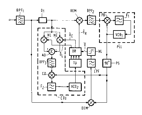
In the receiver shown in Fig. 1,
noise and interference are removed from the received BPSK-signal as well
as posible with the aid of a bandpass filter BPF1 having a centre
7()7
PHN 12.144 4 24.05.1988
~requency equal to the carrier frequency fc = 70 MHz and having a
band width which is chosen such that no appreciable loss of signal power
occurs. In vlew of the width 2/T = 2 MHz of the main lobe of the BPSK
spectrum a (3 dB) bandwidth of approximately 2.5 MHz is a suitable
choice for this band pass filter ~3PF1. The ~3PSK-siynal thus filtered
is col1erent]y c1emodulated in a PSK demodulator DEM which in this case is
constitllted by a multiplier, and the demodulated data signal is selected
Witl1 the aid of a lowpass filter LPF having a transfer chaIacteristic
which is predominantly constant for frequencies up to approximately the
Nyquist frequency 1/(2T) of the binary data signal a(t). A suitable
choice for this lowpass filter LPF is a fourth-order ~utterworth-
Tl1omson filter having a (3 dB) bandwidth of 0.54/T = 540 KHz.
The local carrier of frequency fc necessary for the
coherent demodulation is recovered from the received BPSK-signal using
the principle of PSK-remodulating this ~3PSK-signal in accordance with
the demodulated data signal for producing a carrier component that is
used as an input signal for a phase-locked loop in which a local carrier
generator is included. To obtain a local carrier with the lowest
possible phase jitter, the PSK-remodulation should preferably be
uerformed by using the data signal, regenerated as regards the amplitude
and instant of occurrence, instead of demodulated data signal itself.
In the receiver of Fig. 1, the system for the recovery of
the local carrier, described in the forgoing, is now implemented as
~ollows. The demodulated data signal at the output of lowpass filter LPF
is applied to a hard limiter HL to obtain an amplitude-regenerated
binary data signal a(t) that is subsequently regenerated as regards
instant of occurrence in a binary data regenerator DR which is connected
through a timing unit TU to a generator VC02 for generating a local
clock of bit rate 1/T. Data regenerator DR applies a completely
regenerated, i.e. as regards both amplitude and instant of occurrence,
binary data signal âR(t) to a PSK-remodulator REM for the received
BPSK-signal, the remodulator REM in this case again being constituted by
a multiplier. Since both lowpass filter LPF and also data regenerator DR
introduce a delay, the filtered ~PSK-signal at the output of bandpass
filter ~PF1 is applied to remodulator REM through a delay element D1
to introduce a compensating delay, so that the regenerated data signal
âR(t) is in synchronism with the data signal a(t) that is inherent
707
PHN 12.144 5 24.05.1988
to the filtered BPSK-siqnal applied to the remodulator REM. If, for the
sake of simplicity, ~.he influence of filteriny and the influence of
noise and interference are not consldered and the BPSK-signal applied to
remodulato:r REM is wr.it.ten as
a(t) . sin(2~fct + ~c)
whe~ein ~c is the carrier phase, then remodulation in accordance with
the reyenerated data signal âR(t) results in a slgnal of the form
àR(t) . a(t) . sin(2~fct + ~c)
If no transmission errors occur, âR(t) is equal to a(t) so that,
neglecting a scale factor which is not important here a perfect carrier
reference
sin(2~fct + ~c)
is recovered. However, in actual practice, bit errors always occur in
âR(t) with a given bit error rate and furthermore âR(t) is not
fully bit-synchronous with a(t) due to phase deviations of local clock
generator VC02 which result in a shift of aR(t) relative to a(t)
over a time interval pT (denoted the clock phase error hereinafter). The
absolute value of this clock phase error pT never exceeds T/2 since a
shift of the local clock over a time interval -T/2 is equivalent to a
shift over a time interval +T/2. These clock phase errors and also the
bit errors cause brief sign inversions of the product âR(t).a(t) and
consequently of the carrier component at the output of remodulator REM.
As a result, this carrier component is contaminated by multiplicative
noise and moreover by additive noise and interference penetrating into
the receiver from the input. The output signal of remodulator REM is
therefore first filtered with the aid of a bandpass filter BPF2 having
a centre frequency equal to carrier frequency fc = 70 MHz and having a
(3 dB) bandwidth of, for example, 200 KHz, and is thereafter applied to
a phase-locked loop PI.L in which a signal-controlled generator VC01 is
incorporated for generating a local carrier of frequency fc~ In
addition, this phase-locked loop PLL includes a phase dectector PD for
detecting the instantaneous phase difference between the local carrier
and the signal originating from bandpass filter BPF2, and also a
lowpass filter F1 to obtain a control signal for generator VC01. As
phase detector PD is of the multiplier type, phase lock of this loop PLL
occurs at a noninal phase difference of 90 between the two input
signals of phase detector PD, so that, irrespective of a constant scale
PHN 12.144 6 24.05.1988
factor the local carrier can be written as
cos ( 2~fCt -~ ~o
wherein ~0 is the local carrier phase and the phase error
~e = ~c - ~0 on phase-lock is very small. This local carrier from
generator VCO1 i5 applied to demodulator DEM through a 90 phase-
;hifter PS. So as to effect that the BPSK-signals applied to demodulator
DEM and remodulator REM have an appropriate mutual phase
relationship -the time delay of delay-compensating element D1 must
moreover be rl~osen such that the phase-shift introduced thereby at
carrier frequency fc is an inteyral multiple of 180. This value of
180 results from the fact that phase-locked loop PLL can lock at both
a nominal phase error ~e = and at a nominal phase error ae =
180. On the other hand this phase ambiguity is not a shortcoming of
phase-locked loop PLL but a typical property of all PSK-techniques (cf.
the said Section 11.2 of the book by Gardner). The influence of this
phase ambiguity on the data transmission can be eliminated in known
manner by utilizing differential encoding in the transmitter prior to
the BPSK-modulation and by utilizing differential decoding in the
receiver subsequent to the BPSK-demodulation and the regeneration. This
differential decoding of regenerated data signal âR(t) for the data
transmission proper is not shown in the receiver of Fig. 1 since this
decoding is of minor importance for the present description.
As regards the practical implementation of phase-locked
loop PLL in the described carrier recovery system it should be noted
that its (3 dB) bandwidth is chosen such tl1at also for the maximum
frequency deviations of its input signal to be expected relative to the
nominal value of fc = 70 MHz the loop PLL will still sufficiently
rapidly pass from the non-locked state to the locked state. At frequency
deviations of not more than 5 KHz a value of, for example 20 KHz for
the (3 dB) bandwi~th of loop PLL is amply sufficient. After the phase
lock has been obtained, this (3 dB) bandwidth is reduced to a value of,
for example, 1 KHz to reduce the phase jitter of the local carrier. This
can be effected in known manner by switching resistors in loop filter
F1 under the control of the smoothed output signal of a quadrature
phase detector (not shown in Fig. 1) which in the most current designs
of a phase-locked loop is already present as a locking indicator (cf.
pp. 88-89, of the book by Gardner). In addition bandpass filter BPF2
1~371~7
PHN 12.144 7 24.05.1988
is preferably implemented as d bandpass limiter so as to apply a signal
of constant amplit.~lde to pllase detector PD in phase-locked loop PLL. The
influence of the limiter on the sirJnal-to-noise ratio (SNR) is
restricted to a very small deterioration of not more than 1.05 dB for
very low SNR values at the input (cf. Section 6.11, pp. 125-128 of tl1e
book by Gardner). The phase-shifts occu:rrin~ in bandpass filter BPF2
in response to frequency deviations of its input si~nal relative to its
centre frequency of f~ = 70 MHz always remain limited to very low
values at the selected value of 200 KHz for the (3 dB) bandwidth and the
maximum value of 5 KHz for these frequency deviations.
The attractiveness of the described carrier recovery
system can be demonstrated by comparing this system with two other
systems, whose behaviour is described on pages 226-230 of Gardner s
book. In this comparison, the relevant circumstances are the same for
all systems, that is to say that the same bandpass filter BPF1 and the
same phase-locked loop PLL are used and that in addition the signal-to-
noise ratio SNR in the passband of filter BPF1 has the same value for
all systems. In the first prior art system, an unmodulated carrier is
applied to filter BPF1 and loop PLL is directly connected to the
output of filter BPF1. The second prior art system differs from the
present system in that the demodulated data signal at the output of
lowpass filter LPF is used for the BPSK-remodulation in remodulator
REM. In Gardner s book, the first prior art system is characterized as a
first-order system (N = 1) since the control signal in the loop PLL is
proportional to SEN(~e), wherein ae = ~c - ~0 is the phase
error. The second prior art system is characterized as a second-order
system (N = 2) since the control signal in the loop PLL is proportional
to sin(2~e), and furthermore the influence of the multiplicative noise
on remodulation is represented by a loss factor which increases within
decreasing SNR-values. The behaviour of these two prior art systems is
illustrated in Fig. 11.11 of the book by Gardner by the curves for N = 1
and N = 2. If now i.n the system shown in Fig. 1 it is assumed that the
clock phase error pT is very small, then it appears that for high SNR-
values, for which multiplicative noise on remodulation in response to
bit errors may be neglected, the present system behaves as a first-order
system as the control signal in the loop PLL is proportional to
sin(~e). In addition, it appears that at decreasing SNR-values, a
707
PHN 12.144 8 24.05.1988
510wly increasing deterioration indeed occurs compared with a first-
order system, but that the behaviour of the present system, also at low
SNR-values, is ~till significantlY better than that of a second-order
system.
In order to achieve the improved reliability of the
recovered carrier at low SNR-values, the receiver must indeed have the
disposal of a local clock of bit rate 1/T which is still sufficiently
reliable also at these low SNR-values. In the present receiver a novel
__ concept is now used for the recovery of this local clock from the
received BPSK-signal, which novel concept utilizes both coherent
demodulation with the aid of the local carrier and also correlation of
the data signal a(t) inherent to the received ~PSK-signal with delayed
and advanced versions of the fully regenerated data signal âR(t) so
as to generate a cont~ol signal for local clock generator VC02.
In the receiver of Fig. 1, this novel concept is
implemented as follows. Data regenerator DR and timing unit TU are
arranged to generate both the regenerated data signal âR(t) and also
advanced and delayed versions âE(t) and âL(t) of data signal
âR(t), the advance and the delay both corresponding to a shift a
time interval ~ less than bit interval T. For the case a time interval
= T/4 is chosenl it then holds that
âE(t) = âR(t + T/4) = âL(t + T/2)
A possible practical implementation of data regenerator DR and timing
unit TU for this case is illustrated in Fig. 2 and the associated clock
signals are shown in Fig. 3. Data regenerator DR comprises a cascade
arrangement of four D-flipflops which are interconnected in the manner
shown in Fig. 2. The input of this cascade receives data signal â(t)
at the output of hard li.miter HL in Fig. 1 and the respective
regenerated data signals âE(t), âR(t) and âL(t) areavailable
at the output of the secondl third and fourth D-flipflops. The
respective clock signals CDI CE~ CR and CL for the four
D-flipflops are derived in timing unit TU of Fig. 2 from the local clock
of clock generator VC02 in Fig. 1. This local clock constitutes the
clock signal CD for the first D-flipflop and the furher clock signals
CE, CR and CL are derived from the local clock with the aid of two
delay elements D2, D3 and an inverter which are interconnected in
the manner shown in Fig. 2. The time delay produced by element D3 is
3~ 7
PHN 12.144 g 24.05.1988
equal to the time interval A = T/4. As regards the time delay of element
D2 it should be noted that delay element n1 in Fig. 1 now must al.so
produce a compensating ~elay ~or the time interval ~ - T/4 through which
data signal âR(t) is delayed relative to data siynal aE(t). For
the time delay ~)f element D1 a value of 1.25 T is chosen which
satisfies the r~quirement that the phase-shift produced thereby at
carrier frequency fc is an integral multiple of 180 and is also
adequate]y sufficient to compensate in the formation of data signal
âE(t) fur the time delay of lowpass filter LPF. The difference
between the time delay of this lowpass filter LPF, which is, for
example, 0.625 T, and the duration T of one bit interval is compensated
with the ald of delay element D2 in timing unit TU, this element D2
consequently having in this example a time delay of 0.375 T.
To achieve that regenerated data signal âR(t) is in
synchronism with data signal a(t) inherent to the BPSK-signal applied to
remodulator REM, ]ocal clock generator VC02 in the receiver of Fig. 1
is included in a clock tracking unit CTU which further includes means
which in response to this BPSK-signal and the local carrier generate a
baseband control signal for clock generator VCo2. To that end, clock
tracking unit CTU includes two PSK-remodulators ML and ME which in
this case are again constituted by multipliers. The filtered and delayed
RPSK-signal at the output of delay element n1 is subjected in these
remodulators ML and ME to a PSK-remodulation in accordance with the
delayed version âL(t) and the advanced version âE(t),
respectively, of regenerated data signal âR(t). With the aid of an
adder AD the output signal of remodulator ME is subtracted from the
output signal of remodulator ML and the carrier component of the
differential signal at the output of adder AD is thereafter selected by
means of a bandpass filter BPF3 and coherently demodulated in a
demodulator CD with the aid of the local carrier at the output of phase-
shifter PS. Finally, the baseband control signal for local clock
generator VC02 is obtained with the aid of a lowpass filter F2
connected to demodulator CD.
The main character of this baseband control signal can
now be derived by, as also done in the forgoing, leaving the influence
of filtering and noise out of a account and thus by writing the BPSK-
signal applied to clock tracking unit CTU as
3707
PHN 12.144 10 24.05.1988
a(t) . sin(2~fct + ~c)
Remodulation of this ~PSK-si-Jnal in accordance with the delayed and
advanced version r^lL(t) and âE(t) of regenerated data signal
âR(t) then results in the output signals
âL(t) . a(t) . xin(2~fct + ~c)
âE(t) . a(t) . sin(2~fct + ~c)
of remodulators ML and ME. When phase-locked loop PLL has reduced
the phasc error ~e = ac ~ ~0 to the value zero, so that,
neglecting a constant scale factor, the carrier derived from phase-shift
PS can be written .lS
sin(2~fct + ~c)
then the subtracting operation in adder AD and the subsequent coherent
deomulation in demodulator CD results in a baseband output signal of
shape
âL(t) . a(t) - âE(t) . a(t)
neglecting a scale factor 0.5. In the absence of transmission errors,
regenerated data signal âR(t) is a version a(t+pT) of data signal
a(t), shifted over a time interval pT, pT being the clock phase error
of the local clock. On the basis of the relations between âE(t),
âL(t) and âR(t), the baseband output signal of demodulator CD
can then be written as
a(t + pT - T/4) . a(t) - a(t + pT + T/4) . a(t)
Since lowpass filter F2 forms the average value of this signal over
time interval which is very large relative to the bit interval T, the
olltput signal of this filter F2 is given to a very good approximation
by
a(t + pT - T/4) . a(t) - a(t + pT + T/4) . a(t)
the subscript line symbolizing the mathematical averaging operation. Now
the autocorelation function R(7) of data signal a(t) is defined as
R(~) = a(t) . a(t + r)
so that the output signal of filter F2 and consequently the control
signal for clock generator VC02 can be written as
R(pT - T/4) - R(pT + T/4)
Fig 4 shows the shape of this control signal as a function of the clock
phase error pT for the case in which the symbols of binary data signal
1~37()7
PHN 12.144 11 24.05.1988
a(t) have a waveform of the NRZ-type and assume the values +1 and -1. In
Fig. ~, the two terms of the above expression are shown separately, the
Eirst term being denoted by RL and the second term by -RE, so that
the cc)ntrc)l si-Jrlal is given by RL ~ RE. Since the clock phase error
pT c.~n never exceed T/2, the control signa] is always located in tl1at
portion of the control curve RL ~ RE in Fiy. 4 that is represented
by a fat line.
In the above consideration, filtering of the BPSK-signal
in the transm:itter and in bandpass filters BPF1, BPF3 of the
receiver of Fig. 1 are left out of account. This filtering results in
the shape of the composite parts RL and RE ''f the control curve
deviating from the triangular sl1ape of the autocorrelation function of
data signal a(t) that is shown in Fig. 4, but it will indeed retain
substantially the same character. Consequently, Fig. 4 renlains
representative of the main character of the control curve RL in RE.
As regards the influence of noise, the description of
deriving the control signal brings out an important advantage of the
novel method for recovering the local clock from the received BPSK-
signal. In contrast to other, known methods (cf. pp. 230-249 of the
book by Gardner), tl1is novel method for generating tl1e control signal
for clock generator VC02 does not utilize elements having a non-linear
amplitude transfer characteristic which result in the introduction of
additional noise in this control signal. Thus, it will be possible to
ensure a reliable recovery of a local clock with little phase jitter at
lower SNR-values at the receiver input than in the case these other
known methods are used.
As regards the practical implementation of the system
(CTU, TU, DR) shown in Fig. 1 for the clock recovery it should be noted
that the (3 dB) bandwidth of the loop formed by this system is chosen
such that also for the maximum frequency deviations to be expected of
the clock in the transmission system relative to the nominal value of
1/T = 1 MHz the loop will still sufficiently rapidly pass from the non-
locked state to the locked state. At clock frequency deviations that in
practice will be much less than 100 Hz, a value of, for example, 250 Hz
for the (3 dB) loop-bandwidth is adequately sufficient for that
purpose. Since this loop-bandwidth is predominantly determined by the
bandwidth of lowpass loop filter F2, the (3 dB) bandwidth of
37()7
PHN 12.144 12 24.05.1988
bandpass filter ~PF3 is of minor importance. In the example described,
a :rather arbitrary value of 200 KH~ is chosen for this (3 dB) bandwidth
of bandpass filter BPF3.
After the extensive explanations already given it will be
evident thdt the novel cnncept for cloclc recovery results in an improved
reliability of the recovery of the carrier for low SNR-values at the
input of the receiver. This improved reliability is confirmed by
experiments in which the described example of the receiver of Fig. 1 was
used, in which experiments the SNR-value at the input of the receiver is
indicated by the value, expressed in dB, of the ratio Eb(No)~
wherein Eb is the received signal energy per bit interval T and No
is the spectral power density of additive white Gaussian noise. These
experiments provcd that the present system for the combined recovery of
the carrier and the clock remains in the locked state up to values
values Eb/No of approximately -10 dB, which means an improvement of
4-6 d~ compared with known second-order systems for the recovery of the
carrier.
From the explanations given and also from the block
diagram of Fig. 1 it will be clear that in the present receiver there is
a strong connection between the recovery of the carrier, the recovery of
the clock and the detection of the data signal. Errors in one of these
three processes influence the other two processes. Because of this
strong connection the question arises whether the present system for the
combined recovery of the carrier and the clock can change from the non-
locked state to the locked state. This question can be answered in theaffirmative, as, at a deviating clock frequency, the clock phase error
pT cannot become greater than T/2, as was explained in the foregoing.
When in this case the carrier loop PLL is in the locked state, the
probability of incorrectly detected data bits at values Eb/No which
are not too low will not become greater than 0.25. In this situation
there still is at the output of remodulator REM a carrier component
having a sufficient power for a reliable recovery of the carrier. So
clock recovery is in principle not necessary for the carrier recovery.
In contrast thereto, to enable clock recovery, a recovered carrier is
indeed necessary for the coherent demodulation in demodulator CD of
clock tracking unit CTU. When the carrier loop PLL is in the non-locked
state, for example on switch-on of the receiver, the carrier phase error
7()7
PHN 12.144 13 24.05.1988
~e as a function of time will vary with a frequency equal to the
frequency difference between the two input signals of phase detector
PD. If this frequency difference is mllch maller than the clock
frequency 1/T, which generally is the case, this phase error e varies
from 0 to 360 in a manner that is slow compared to the bit rate
1/T at whicl, the data signal varies. During one period (of 360) of
this v~}ying phase error ~e many data bits are detected, however with
an error rate which depends on clock phase error pT and carrier phase
_-eIror ~e During this 360 period two ranges occur in which data
bits are detecte~ with a minimum error rate, more specifically the
ranges around the values ~e = and ~e = 180. These ranges are
stable points onto which the carrier loop PLL can lock, since the
variation of the phase error ~e is very slow compared to the variation
of the data signal of the bit rate 1/T and consequently a sufficient
number of data bits is correctly detected to produce at the output of
remodulator REM a carrier component having a sufficient power to bring
the carrier loop PLL into the locked state. After locking of the carrier
loop PLL a reliably recovered carrier is available for the coherent
demodulator CD in clock tracking unit CTU, so that also the clock loop
(~TU, TU, DR) can lock. Thus, the combined system for the recovery of
the carrier and the clock has been brought in its totality from the non-
locked state into the locked state. From said experiments with the
described example of the receiver of Fig. 1 it was found that, after
loss of lock, the present system for the combined recovery of carrier
and clock again reaches the locked state for values Eb/No greater
than approximately -6 dB.
The performances of the present system are clearly
visible in Fig. 5 which shows the bit error rate (BER) as a function of
Eb/No. In view of the phase ambiguity already mentioned (phase-
locked loop PLL can lock at ~e = or at ~e = 180), the BER-
value shown in Fig. 5 does not relate to the bits of regenerated data
signal âR(t) used for the BPSK-remodulation, but to data bits which
were derived from the bits of âR~t) by means of differential
decoding, differential coding being used in the transmitter for forming
the bits of data signal a(t). The broken-line curve in Fig. 5 shows for
these differentially decoded data bits the BER-values which are
theoretically feasible. The solid-line curve in Fig. 5 represents the
i7()7
P~IN 12.144 14 2~.05.1988
BER-values measured ~or tl~e nne (asc in l:hc exL)~rLm~nt:; already
mentioned in the foregoing. Fig. 5 shows that, i.n comparison with the
theoretic,ll situation, the present system results in a slight
deterioratic)n which is less than 1 dB. In addition, it appears that also
at very low values for Eb/No the data bits can still be detected. Of
collrse the BER--value is then relative]y high, but the influence thereof
(~an effective~y be combated by means of error-correcting codes as long
as the present system remains in the locked state, which, as has been
mentioned al~eady, is the case up to values Eb/No of approximately -
10 dB. These experiments also show that the present system is ratllerinsensitive to disturbing signals. It was found more specifically that
tlle present system always remains in the locked state as long as the
power of an interfering carrier at the input of the receiver is less
than the received power o~ the desired signal, even for interfering
carriers having a frequency near the carrier frequency fc = 70 MHz of
tlle desired signal.
So far the system for tlle combined recovery of the
carrier and the rlock has been described for the case of a BPSK-
signal. The present invention is however not limited to BPSR-signals, as
tl1e same principles can also be applied to other types of PSK-signals.
This will now be described by way of example for the case of a receiver
for quarternary PSK-signals (denoted as QPSK-signals or as four-phase
signals).
This explanation can be a short explanation, as a
receiver for a QPSK-signal basically only differs from the receiver
shown in Fig. 1 for a BPSK-signal in that demodulator DEM and
remodulator REM in Fig. 1 are replaced by tl1eir QPSK-equivalents, which
are known Per se, in the manner shown in Fig. 11.8 on page 223 of the
book by Gardner. As regards demodulator DEM this implies tllat the output
of filter BPF1 is connected to a second amplifier to which the
quadrature-phase carrier (which is already available at the input of
phase-shifter PS) is applied and from which, with the aid of a second
lowpass filter (which corresponds to lowpass filter LPF) a second
demodulated data signal is derived which is inherent to the quadrature
component of the QPSK-signal. The second data signal is thereafter
regenerated as regards amplitude and instant of occurrence, with the aid
of a second hard-limiter (corresponding to hard-limiter HL) and a second
l;~c~;~7(~7
PHN 12.144 15 24.05.19~8
data generator (which differs from data regenerator DR in that the last
D-flipflop in the cascade arrangement can be omitted and vnly the output
of the third D-~lipflop is utili~ed), the second data regenerator also
being controlled by timing unit TU (with the exception of clock signal
CL whicl1 is now superfluous). As regards remodulator REM, this means
that the output of delay element D1 is also connected to a second
multiplier for remodulating the QPSK-sirJnal in accordance with the
regenerated second data signal for producing a second carrier component
which, through a -90 phase-shifter, is added by means of an adder to
the carrier component which hdd already been obtained at the output of
the fi.rst multiplier, whereafter the output signal of this adder is
applied to bandpass filter BPF2. The carrier loop PLL and the clock
tracking unit CTU need, however, not to be modified.
In addition, the possibility is pointed out to implement
within the frame work of the invention the clock tracking unit CTU in a
manner other than the manner shown in Fig. 1. From the explanation of
clork unit CT4 of Fig. 1 as given in the foregoing, it will be apparent
that for instance the order of the operations performed in oherent
cdemodulator CD on the one hand and the combination of remodulators ML,
ME and adder AD on the other hand can be interchanged, so that first
the coherent demodulation and thereafter the multiplication by the
delayed and advanced versions âLtt) and âE(t) of regenerated
data signal âR(t) are performed. Of course a lowpass filter
connec-ted to the output of the displaced demodulator CD must be
substituted for bandpass filter ~PF3, and the delay produced by such a
filter must be taken into account of in the choice of the connecting
point of clock tracking unit CTU for receiving the filtered and,
optionally, delayed BPSK-signal at the output of bandpass filter
BPF1. This measure and further measures necessary for maintaining the
desired time and phase relationships between the different signals in
the receiver of Fig. 1 are fully within the scope of a person skilled in
the art and, after taking cognizance of the foregoing description need
no further explanation. It should however be noted that from the point
of view of practical implementation, preference is given to the design
of clock tracking unit CTU shown in Fig. 1.
Finally it should be noted that it is possible to
implement, in the event of QPSK-signals, the remodulators ML and ME
37(~7
PHN 12.144 16 24.05.1988
also for QPSK-remodulation in the manner already described for
remodulator REM. After the extensive descriptions already given in the
foregoin~ also this pos;ibili.ty needs no further explanation.