Note: Descriptions are shown in the official language in which they were submitted.
1~3~
20104-8265
The inventlon relates to a method of optlcally recording
and erasing information in which a disc-shaped recording element
which comprises a substrate and a recording layer provided thereon
which comprises crystalline recording material is rotated and
exposed to the light of a recording spot which is moved
diametrically over the disc and originates from a laser light beam
which is focused on the recording layer and is modulated in
accordance with the information to be recorded, amorphous
information bits being formed in the exposed places of the
recording layer which bits can be read by means of weak laser
light and which can he erased by means of an erasing spot
originating from a laser light beam focused on the recording
layer.
Such a method which thus is based on crystalline-
amorphous phase changes is known, for example, from European
Patent Application No. 0,135,370 published on March 27, 1985 in
the name of Hitachi, Ltd., and from the copending Netherlands
Patent Application No. 8403817 published on July 16, 1986 in the
name of the Applicants. In the known method a Te-Se alloy is used
as a recording material which may comprise other elements. This
method has for its disadvantage that the erasing time, i.e., the
exposure time which is necessary to return the amorphous
information area (bit) to the original crystalline phase, is long.
For example the erasing time of a Te-Se-Sb alloy is, for example,
50 ~s.
During the recording of information, the reading thereof
and erasing the information the recording element is rotated. The
linear speed of the element is, for example, from 1 m/s to 15 m/s
or more. Upon recording audio (sound) information according to
the EFM (eight out of fourteen) modulation system, a linear disk
(element) velocity is used of 1.4 m/s. In video information a
~.
Z
PHN.11703 2 7-3-1987
linear spee~l o~ 10-15 m/s is used.
It is highly desirable to perform the erasing
process at the same linear disk speed as the recording
process, that is erasing in rea:L time. Furthermore it
is highly desirable to be able to erase the information
during one rotation of the element. For practical appli-
cations this presents the very interesting possibility
of recording new information directly over the existing
information, in which after the existing information has
lO been erased, the new information can be recorded imme-
diately thereon at the same disk speed and in the same
rotation run of the element. Such a direct overwrite
cannot be realised in magneto-optical recording processes,
in which at least one complete revolution of the recording
15 element exists between erasing and re-recording.
In phase change recording with the above-mentioned
erasing time of 50/us, an erasing process in real time
with one revolution of the element also is not readily
possible in practice. Even at a very low linear disc speed
20 of 1.4 m~s a slot-shaped erasing spot having a minimum
length of 70/um must already be used in that case. The
erasing spot is the light spot of the laser light beam
on the recording layer used in the erasing process.
An erasing spot of 70/um meets with considerable practical
25 disadvantages due to the required high laser power, as well
as the positioning of the spot on the track. At higher
disc speeds even an erasing spot having a length in the
order of magnitude of mm is necessary, which cannot be
performed in practice.
In the published Japanese Patent Application
Kokai 60-177446 an optical recording medium is described
the recording material of which satisfies the formula
In1 XSbx My wherein M is selected from a group of 13
elements, substantially metals, x is 55-80 % by weight
35 and y = 0-20 % by weight. Upon recording information,
the recording material is exposed to modulated laser light.
In the exposed places, depending on the rate of cooling,
either a semi-stable phase is formed which is termed ~-phase,
lZ~3~73Z
PHN.11703 3 7-3-1987
or a mixed phase of InSb and Sb. The ~phase can be trans-
ferred to the mixed phase by heating. So there is switched
- i.e. recording and erasing process - between a mixed
phase and a ~ phase. This has for its disadvantage that
upon converting the mixed phase two constituents are
concerned. As a result of this the number of switching
times - recording and erasing - is restricted although,
according to the Kokai, a repeated reproduction is
possible. This is a stability problem which for the
practical application is not acceptable. Moreover, the
speed of conversion of the mixed phase to the ~ phase
is limited because the two components InSb and Sb must
find each other in the good proportion before conversion
takes place. In the said Kokai no information is given
15 or details disclosed of the erasing process, particularly
the speed of erasing and the quality of the erasing process -
the magnitude of a possible rest signal. It is stated that
the information can be removed by "scanning" with laser
light.
A further serious disadvantage is the low signal-
to-noise ratio of the information bits, which does not
enable video recording.
It is an object of the invention to provide an
optical recording method of the type mentioned herein-
25 before in which very short erasing times can be used and
in particular the recorded amorphous information bits
can be erased in real time during one revolution of the
recording element.
A further object is to provide an optical
30 recording method in which the recorded information bits
can be read with a very high signal-to-noise ratio which
on an average has a value of 5O dB and higher as a result
of which video recording is possible.
Still another object of the invention is to
35 provide an optical recording method having a high quality
of both the recording and the erasing process. The recor-
ding process can be carried out at a high recording speed
and with a high information density. By means of the
1~3'7~
PHN.11703 4 7-3-1987
erasing process the recorded information bits are erased
to a negligible rest signal so that recording and erasing
can be carried out many times and high signal - to-noise
ratios are st-ill obtained.
According -to the invention these objects are
achieved by means of a method of the type mentioned in
the opening paragraph which is characterized in that a
recording material is used the composition of which
satisfies the formula
QxSbyTe
wherein Q is the element In or Ga,
x = 34-44 at./O; y = 51-62 at. /0; z = 2-9 at. /0,
that the amorphous information bits recorded in the
crystalline recording material can be erased in real time
15 during one revolution of the recording element by means
of the erasing spot and thereby returned to the original
crystalline state.
Very short erasing times of, for example, 100 ns
or even shorter, can be realised by means of the method
20 according to the invention. The recording material used
in the method according to the invention presents the
important advantage that the erasing time necessary to
crystallize an amorphous area can be adjusted and first
of all depends on the selected quantity of Te within the
25 indicated limits. With comparatively small quantities of
Te, for example, an atomic percentage smaller than 5 /0,
a very short erasing time is obtained. By choosing a
higher percentage of Te, a longer erasing time can be
adjusted, hence a lower crystallisation rate. A lower
30 crystallisation rate is of importance when the recording
rate is low, hence at a comparatively low speed of the
element. It is hence possible at the different speeds of
the element, in accordance with the use of the element for
audio recording, video recording and data recording, not
35 to adapt or to adapt not exclusively the size of the
erasing spot but to adapt the erasing time by a variation
of the Te content of the recording layer. The limits of
the Te content are 2 and 9 at. /0. With a Te content
;3~3Z
PHN.11703 5 7-3-1g87
smaller than 2 at. /0 the crystallisation rate is so high
that no crystalline amorphous changes are possible any
longer and the recording process no longer operates. With
Te contents exceeding 9 at. % the crystallisation rate is
so low that erasing in real time can no longer be carried
out adequately.
With an Sb content exceeding 62 at. /0, elementary
Sb is deposited so that the system is no longer stable.
With an Sb content lower than 51 at. /0 the crystallisation
rate becomes too high so that the recording process
(crystalline to amorphous) is no longer satisfactory. If
the Q content is lower than 34 at. /0, the system becomes
unstable. With a Q-content exceeding 44 at. /c the
crystallisation rate is too high so that the erasing
15 process occurs excellently, it is true, but recording
information in which there is switched from crystalline
to amorphous is no longer possible or is possible with
extreme difficulty only. Very good results are obtained
in particular when the Te and Sb contents together amount
20 to 58-65 at. % and more in particular to 58-62 at. /0.
The composition of the recording layer may be
chosen to be so that extremely short erasing times are
realised, hence high crystallisation rates. Such a material
can be erased at any disc speed. However, it is to be
25 preferred in order to promote the recording process to
use, at lower disc speeds, a material having a longer
crystallisation time.
The recording layer used in the method according
to the invention has an excellent stability, not only in
30 the crystalline phase but also in the amorphous phase. The
stability of the amorphous phase against crystallisation
has been established by means of a standard DSC (differen-
tial scanning calorimetry) test. It has been found that
54 e6 e crystallisation time of
35 the amorphous phase at 50C is 3 x 10⁵ years. At 100C the
crystallisation time is 8 years. So there is a very great
stability.
3'~Z
PHN.11703 6 7-3-1987
In a preferred form of the method according to
the invention a recording material is used the composition
of which satisfies the formula
Inx~sby~Te ,
wherein x' = 35-42 at. /0; ~' = 52-60 at. /0; z~ = 3-8 at. %.
In this preferred form very high signal-to-noise
ratios are obtained with average values of 50-55 dB and
highest values of 60 dB. It is to be noted that when
replacing Te by Se the signal-to-noise ratios show a
lower value.
Excellent results are obtained in particular
in a further preferred embodiment of the method in accor-
dance with the invention in which a recording material
is used which satisfies the formula
I~X,ISbyllTez~
wherein x" = 37-42 at. /0; y" = 52-56 at. /0; z" = 5-8 at. %.
The linear speed of the rotating recording
20 element depends on the type of information which is recor-
ded, for example audio information, video information or
data information, and is, for example, from 1 to 20 m/s.
During the recording process the crystalline recording
material is heated above the melting temperature in the
25 exposed places so that a melting area is formed which
cools so rapidly that no crystallisation takes place and
an amorphous information bit is formed. The information is
recorded at high speed. The pulse time of the laser light
beam in which per pulse an information bit is formed, is
30 short and is, for example, from 20 to 100 ns. The formed
amorphous information bits have small diametrical dimensions
from at most one to a few micrometres so that a high
information density is obtained.
In the erasing process the amorphous information
35 areas (information bits) are exposed to the erasing spot.
As a result of this an amorphous area is heated to a
temperature which is slightly lower than the melting-
point of the material in the crystalline phase but higher
lZ~3~32
PHN.11703 7 7-3-1987
than the glass transition temperature. As a result of this
the amorphous material of such an area becomes less viscous
and will return to -the thermodynamically more stable
crystalline state. The material will have to be kept at
the above-mentioned temperature for some time (erasing
time) so that all the material in such an ~rea crystallises.
The method according to the invention surprisingly
represents the possibility of using very short erasing
times. In a preferred form of the method the erasing time
l per information area is from 50ns to 5/us and in particular
from 100 ns to 1/us.
In a further preferred form of the method in
accordance with the invention an erasing spot is used
which is circular or elliptical and has a maximum dia-
l5 metrical or longitudinal dimension of 3/um. In particulara circular erasing spot is used having a diameter of 1-2
um. The required laser power is lower then. Such a small
circular erasing spot, compared with a slot-shaped erasing
spot, presents the further advantage of a better focusing
20 on the recording layer and a better control and guidance
over the information track. Moreover, the optical device
for performing the method is technically simpler in case
of a circular erasing spot.
To this connection it is noted that the recording
25 element, in behalf of a good control of the recording and
erasing process, preferably comprises an optically detect-
able, spiral-like track. This track is present, for example
in the form of a groove in the surface of the substrate
on the side of the recording layer. In the case of a
30 substrate of a synthetic material the groove can be provided
during the manufacture of the substrate. A suitable manu-
facturing process is an injection moulding or a compression
moulding process in which the hot liquid synthetic material
is injected in a mode which comprises a matrix which at
35 its surface has the negative of the desired groove structure.
In the case of a substrate of, for example, glass, the
groove is provided in a separate layer of synthetic material
on the surface of the substrate. The groove is optically
~Z~ 7~2
PHN.11703 7-3-1987
detected by means of laser light which is shown in via
the transparent substrate. The light reflected against
the recording layer shows phase differences depending on
whether the light is reflected against a groove part or
against a land part present beside the groove. The infor-
mation recorded in the recording element usually lies
in the groove part of the recording layer so that a spiral-
like information track is formed.
A circular small erasing spot can easily be
lO kept on the information track. In the case of a slot-shaped
erasing spot the possibility exists that with some rotation
of the spot an adjacent spiral part of the information
track is exposed and an undesired erasing process takes
place.
Recording and erasing information is carried
out by means of a laser light beam which is preferably
focused on the recording layer via the substrate. Herewith
it is achieved that dust particles or scratches present
on the substrate fall beyond the depth of focus of the
20 focusing objective so that said contaminations do not
influence the quality of recording and erasing. The substrate
in that case must be transparent and be manufactured, for
example, from glass or a transparent synthetic material,
for example, polycarbonate or polymethylmethacrylate.
The circular small erasing spot may be used at
all usual speeds of the recording element because, as
already said hereinbefore, the composition of the recording
layer can be adapted to the exposure time in the erasing
process determined by the spot size and the disc(element)
30 speed. At a low disc speed of, say, only 1.5 m/s and a
spot size of 2/um, for example, which means an exposure
time of 1.3/us a composition of the recording layer can
be chosen having a comparatively high content of the
element Te. This material has a comparatively low crys-
35 tallisation speed. At a disc speed of 15 m/s and an erasingspot size of 2/um, hence with an exposure time of approxi-
mately 135 ns, a recording layer will be used which has a
comparatively low content of the element Te, hence crys-
1'~kt3~73Z
PHN.11703 9 7-3-1987
tallises more rapidly and consequently has a shor-t erasing
time.
A further favourable embodiment of the method in
accordance with the invention is characterized in that
the substrate is provided by means of an electroless
deposition process with an amorphous recording layer in
which by using the erasing spot a spiral-like track of
crystalline material is formed, which track has a width
of a few microns, amorphous information areas are then
formed in the said track by means of a pulsed recording
spot and can be converted again selectively by means of
the erasing spot into the cr~stalline phase and be erased.
A suitable deposition process is a vapour-
deposition process at reduced pressure or a sputtering
l5 process in which an amorphous recording layer is obtained.
Said favourable embodiment presents the advantage that
not the whole recording layer need be converted in one
separate treatment step from the amorphous to the crystal-
line phase.
An erasing spot is preferably used which is
followed at a short distance by the recording spot.
A suitable mutual distance is, for example, from 5-50/um.
Herewith the possibility is presented to record new in-
formation directly over old information.
Another preferred embodiment is characterized
in that the erasing spot and the recording spot originate
from the same laser in which during the recording process
the laser is switched at a higher power and is pulsed.
The invention will be described in greater
30 detail with reference to the drawing, in which
Fig. 1 is a cross-sectional view of a recording
element used in the method,
Fig. 2 is a plan view of a segment of the
Figure 1 element, and
Fig. 3 is a diagrammatic cross-sectional view
of a device ~or carrying out the method according to the
invention,
lZ~3~2
PHN.11703 10 7-3-1987
Fig. Ll is a plan view of a part of the recording
elernent use~ in -the Figure 3 device,
Fig. 5 is a plan view of -the laser set up in the
device shown in Fig. 3,
Fig. 6 is a composition diagram of the elements
In, Sb and Te, and
Figures 7 and 8 show graphically a recording
and erasing process.
Reference numeral 1 in Fig. 1 denotes a glass
substrate. The substrate has the form of a circular disc
having a diameter of 30 cm and a thickness of 1-2 mm.
The surface of` substrate 1 comprises a layer 2 of a UV
light-cured acrylate synthetic resin in which a spiral-
like groove 3 is provided. The groove has a width of 1.6/um
15 and a depth of 60 mm. Lacquer layer 2 with groove 3 has
been manufactured by providing substrate 1 with a layer
of a liquid, UV-curable lacquer, pressing the assembly
against a matrix surface which comprises a groove struc-
ture, exposing the liquid lacquer layer to UV light via
20 the substrate and removing the assembly of substrate
with cured lacquer layer in which the groove structure
has been copied from the matrix surface.
A recording layer 4 of In40Sb54Te6 is vapour-
deposited on lacquer layer 2 at a pressure of 3.10 5
25 Torr by means of a flash evaporator. The rate of deposition
is o.6 nm per second. The thickness of the vapour-deposited
layer 4 is 100 nm. During the vapour deposition the sub-
strate 1 is rotated at a frequency of 20 Hz.
The recording layer is covered with a protective
30 layer 11 of a synthetic resin.
After the vapour deposition the layer 4 has an
amorphous structure. The groove part 5 of the recording
layer is exposed to a continuous laser light beam 6
which is focused on the recording layer 4 via the substrate 1.
The laser used has a power of 5 mW on the recording layer 4.
The laser light beam produces a light spot on the recording
layer, the so-called erasing spot, which is circular and
lZ1~3~ Z
PHN.11703 11 7-3-1987
has a cross-section of 2/um The erasing spot follows the
groove part 5 by using a servo system (control system)
not shown in which a weak laser light beam is used which
is reflected via the substrate 1 against the layer 4 and
which on the basis of phase differences between reflected
light originating from groove 5 and land part 7 scans
the groove structure. During the exposure with the erasing
spot the disc 1 is rotated in which the linear speed
at the area of the erasing spot is 5 m/s. As a result of
the exposure to the erasing spot a track 8 of a crystalline
recording material is formed in the groove part 5.
Said conversion from amorphous to crystalline takes place
during one revolution of the disc 1 hence one passage
past the erasing spot.
During or after said erasing run information
can be recorded in track 8. For this purpose, track 8 is
focused to pulsed laser light 9 which is focused on the
track 8 v the substrate 1. The pulsed laser light beam
9 gives a light spot (recording spot) on the recording
20 layer 4 at the area of the crystalline track 8. The light
spot is circular and has a diameter of 2/um. The pulse
time is 100 ns. The laser light energy per pulse is o.6 nJ.
The laser light beam 9 is controlled and kept on track 8
by means of the above-mentioned servo system, not shown.
25 During the recording of information disc 1 is rotated,
the linear speed at the area of the recording spot being
5 m/s. Erasing and writing takes place in real time during
one revolution of the disc. This may be the same revolution.
For obtaining the recording spot the same laser may be
30 used as is used in the erasing process. Said laser is then
switched temporarily to a higher power in behalf of the
recording process and in addition is pulsed. Alternatively
a second laser may be used for the recording process.
In that case the recording spot can follow the erasing
spot at a very short distance, for example a distance of
30/um. As a result of the exposure to the recording spot,
amorphous information areas 10 (see Fig. 2) having a
diameter of approximately 1/um are formed in the crystalline
1~3~2
PHN.11703 12 7-3-1987
track 1. The information areas 10 can be erased selectively
and hence be converted again into the crystalline phase
by using the above-described erasing spot. Erasing occurs
in real time at a linear disc speed of 5 m/s. The erasing
time per amorphous area is 400 ns. The amorphous information
areas are read by means of a weak continuous laser light
which is reflected against the recording layer 4 via the
substrate 1. Reading is based on reflection differences,
i.e. differences in intensity of the reflected light,
between an amorphous information area and the crystalline
surrounding thereof (track 8).
The above erasing-writing process has been
repeated 400 times wlthout any problems occurring.
In the same manner as stated above information
can be recorded and erased at a different speed of sub-
strate (disc) 1, for example a recording speed of 12 m/s.
In that case an erasing spot is used having a circular
shape and a diameter of 2/um originating from a laser
having a power of 16 mW on the recording layer. In the
selected erasing of the recording amorphous information
areas the erasing time per information area is approximately
170 ns. Information is recorded by means of pulsed laser
light at a pulse time of 55 ns and a pulse energy of
o.6 nJ.
Experiments have demonstrated that the rapid
recording-erasing process can be repeated 800 times
without any problems.
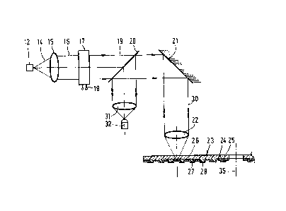
Reference numeral 12 in Fig. 3 denotes a laser.
Parallel to laser 12 a second laser 13 is arranged (see
Fig. 5). The light beam 14 of laser 12 passes through a
lens 15 and is converted into a parallel beam 16, which
then passes through a modulator 17. The modulator serves
as a light shutter controlled by binary (digital) signals
on connection pins 18. The electric signal represent the
information to be recorded. The laser light beam 16 when
passing through modulator 17 is pulsed in accordance with
the binary information to be recorded. It is also possible
to pulse laser 12 directly, without the interconnection of
lZ~3~
PHN.11703 13 7-3-1987
a separate modulator, in accordance with the da-ta to be
recorded. This is the case when an AlGaAs laser having
an emission wavelength of 850 nm is used. The pulsed
laser light beam 1g passes through a semipermeable mirror
20 and is then rotated through 90 by reflection against
mirror 21. The beam 19 is focused by an objective 22 on a
recording element 23 which corresponds to the recording
element shown in Figs. 1 and 2. The recording element 23
comprises a substrate 24 of glass which has a lacquer
10 layer 25 in which a groove 26 is provided. Between the
grooves a land part 27 is present. Lacquer layer 25 compri-
ses a recording layer 28 as stated in the description of
Figs. 1 and 2. The pulsed laser light beam 19 is focused
in the groove part of the recording layer 28 via the sub-
15 strate 24 and produces a pulsed light spot (recording spot)29 on the recording layer (see ~ig. 4). The recording ele-
ment 23 is rotated about the axis 35 in which the linear
speed of the element at the area of the recording spot
is adjusted at a value which generally is between 1 and
20 15 m/s-
In the places exposed to the recording spot 29amorphous information areas are formed as was explained
with reference to Figs. 1 and 2. The amorphous information
areas are read with weak continuous laser light which
25 is focused on the groove part 26 of recording layer 28
according to the same optical path as shown in Fig. 3.
The reflected light beam 30 is intercepted in detector 32
via mirror 21, semipermeable mirror 20 and lens 31, in
which the place and length of the information areas are
30 determined on the basis of reflection differences and
converted, for example, into an electric signal.
The amorphous information areas are present
in a track of a crystalline material provided in the
groove part 26 of the recording layer 28 by using an
35 erasing spot 33 (Fig. 4). In the situation shown by Figs.
3, 4 and 5 the erasing spot originates from a second laser
13 which produces a continuous light beam 34 which traverses
substantially the same light path as beam 14, with the
~3~Z
PHN.11703 14 7-3-1987
proviso that the produced eras:ing spot 33 has been displaced
over a distance of approximately 30/um with respect to the
recording spot 29. The erasing spot 33 precedes the re-
cording spot 29 so that first a crystalline track is formed
in the amorphous recording layer and the amorphous infor-
mation areas are then provided herein. The amorphous
information areas can be erased selectively by the erasing
spot in real time during one revolution of the element
by the conversion into the crystalline phase.
Fig. 6 shows a composition diagram In, Sb, Te
having at the corners of the composition triangle the
indicated compositions In30Sb70; In30 50 20
In50Sb50. The triangle shown hence is a small part of
the total In, Sb, Te diagram. Within the composition
triangle the solid line A denotes a composition area
which corresponds to that stated in Claim 1. The broken
line B denotes an area which is equal to the composition
area as claimed in Claim 3 and the broken line C is a
composition area as claimed in Claim 4. A representative
20 number of specific compositions which has been used by
the Applicants in the method according to the invention
are indicated by dots. ~or convenience said compositions
are summarized hereinafter in table form arranged according
to an increasing In content (in at. ~).
7~2
PHN.11703 15 7-3-1987
Composition table be]onging to Fig. 6.
. ,, . . _ _ ._
In S~ Te In Sb ~e In Sb Te
34.8 61.6 3.6 38.8 55.1 6.1 40.0 54.0 6.o
35.0 60.0 5.0 3g.0 54.9 6.1 40.0 52.0 8.o
10 35.0 57.0 8.0 39.2 5~1.8 6.o 40.3 53.0 6.7
36.2 57.7 6.1 39.3 55.1 5.6 41.0 52.0 7.0
37.1 60.0 2.9 39.4 54.0 6.6 41.5 53.5 5.0
15 37.2 58-5 4.3 39.4 54.7 5.9 42.o 52.0 6.o
38.0 57.0 5~ 39.6 53.6 6.8 42.1 56.o 2.9
20 38.2 54.0 7.8 39-7 54-5 5-9 43.6 52.0 4.4
3~.6 55.2 6.2 40.0 55.8 4.2
The signal-to-noise ratios of the compositions
25 comprised by line A have an average value of 45-50 dB.
In the area determined by line B an average value of
50-55 dB is reached. The most interesting composition
area is represented by line C. Herein highest values of
60 dB are reached. If Se is used instead of Te slightly
30 lower values are obtained.
Fig. 7 shows a graph in which the signal-to-
noise ratio is plotted in dB against the energy used for
making an amorphous information bit. It may be read from
the graph, for example, that an information bit obtained
35 by using a laser light energy pulse of 0.8 nJ has a
signal-to-noise ratio upon reading of approximately 55 dB.
The tests are made in the recording material In41Sb52Te7.
Z
PHN.11703 16 7-3-19~7
The amorphous information bits are recorded in a track of
a crystalline material obtained by exposing the recording
element during one revolution to a circular light spot
originating from a laser having a power of 3 mW. The disc
speed is 1.4 m/s. The wavelength of the laser light is
750 nm. The numerical aperture of the optical focusing
system is 0.5. Upon writing the amorphous information bits
the same laser but then pulsed was used. The laser was
switched at various powers (mW) in order to provide the
quantities of energy per pulse indicated in the graph. The
pulstime in all cases was 60 ns.
In Fig. 8 the decrease of the signal-to-noise
ratio in dB is plotted against the erasing power of the
laser used in mW. The laser has a wavelength of 750 nm.
l5 The numerical aperture is 0.5. The disc speed is 1.4 m/s.
The erasing process was carried out by means of a circular
erasing spot having a diameter of 2/um. The graph indicates
the change as a result of only one erasing run, hence one
passage of the erasing spot over an information bit.
20 It can be read from the graph that in one erasing run the
signal-to-noise ratio has reduced to substantially 0
already with a laser power of slightly more than 4 mW.
When using even lower erasing powers, for example 3mW,
a signal-to-noise ratio of 15 dB is present after one
25 erasing run which is then reduced to zero in a subsequent
erasing run.
An important aspect of the method in accordance
with the invention is that EFM modulated signals can be
recorded and read perfectly. An EFM modulated signal is
30 also used, for example, in the well-known Compact Disc.
By means of the invention, Compact Disc information can
h~nce be recorded and read also at the same disc speed as
used in Compact Disc, namely 1.4 m/s. Such a compatibility
is of technical importance. EFM modulation means that
35 amorphous information bits are recorded in the recording
layer which have, for example, the form of an ellipse and
have different accurately defined, discrete, longitudinal
dimensions of 0.9; 1.2; 1.5; 1.8; 2.1; 2.4; 2.7; 3.0 and
37~Z
PHN.11703 17 7-3-1987
3.3/um. The use of the method according to the invention
makes this possible. The infcrmation bits of the above-
mentioned dimensions may furthermore be scanned, distin-
guished and hence be read with a great accuracy by means
of a laser light beam.