Note: Descriptions are shown in the official language in which they were submitted.
lZE~3736
PHF 84516 1 1,2,1985
Digital-to-analogue converter arrangement,
The present invention relates to a digital-to-
analogue converter arrangement formed on the basis of a
digital-to-analogue converter of a type producing at its
output an output voltage V'(N'~ such that :
(1) V'(n') = k,E, M~
where k is a constant, E is a voltage applied to a
reference voltage input, n' is a binary number applied
to an input for binary signals and M' is the maximum value
n' can attain.
This type of converter arrangement is very
advantageous for signal processing applications,
~ ecause of the linearity of equation (1), the
steps by which the voltage V develops result in an
imprecision which is relatively greater for small amplitu-
des of the value V than for the large amplitudes, If a
high precision for weak amplitudes is required, a digital-
to-analogue converter circuit must be used in which "n"'
is formed from many binary elements,
The invention has for its object to provide a
digital-to-analogue converter arrangement providing a
high precision for a low-amplitude output voltage without
utilizing a binary number "n "' formed from many binary
elements, To that end, a digital-to-analogue converter
arrangement of the above-defined type is characterized in
that it comprises a negative feedback network arranged
between the reference voltage output and input,
Such a network may produce non-linearities
between the output voltage and the number "n "' ; these
non-linearities are not always desirable. In accordance
with an important characteristic of the invention~ a
digital-to-analogue converter arrangement according to the
invention is further characterized in that transcoder means
PHF 84516 2 1~3736 1.2.1985
are provided which, starting from a number "n~' whose
maximum value can reach M, adjust such a num~er "n"' that
a "pseudo-linear" relationship is established between
the number "n" and the voltage V' :
V' (np) = K.-~ (2)
where K is a constant and n ar~e specific values of n.
A "pseudo-linear" relationship must be under-
stood to mean a relation which is only linear for certain
values np of "n". This notion will be explained in greater
detail in the sequel of this description.
he following description which is given by way
non-llmi~ ~ example with reference to the accompanying
drawings will make it better understood how the invention
can be put into effect.
Figure 1 shows a circuit diagram of a digital-
to-analogue converter arrangement according to the
invention.
Figure 2 illustrates the shape of the "staircase"
curve which represents the voltage V as a function of the
number "n".
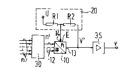
Figure 1 shows the digital-to-analogue
converter arrangement according to the invention. It is
formed around a digital-to-analogue converter circuit 10,
for example an integrated circuit of the type NE 5020
produced by Signetics. With a voltage V' at output 13 there
must correspond a binary number n' applied to input 12
according to :
V~ = k.E. nM,
30 where k is a constant and E is the voltage applied to its
reference-signal input 14,
M~ is the maximum value the number n~ can assume~
M' has the form :
M' = 2 -1
35 where b represents the number of binary elements of the
number n'.
- By way of example, let it be assumed that such
a converter arrangement is used in radio-navigation to
PHF 84516 3 lZ~3736 1,2.1985
apply a control voltage to an a:Ltimeter derived from a
digital information processed by a radio altimeter. The
object i5 to supply a voltage between 0 and 25 Volts for
altitudes comprised between 0 and 5000 ft with a
5 resolution better than 0.5 ft near 0, that is to say that at
this level the voltage must evoLve in steps of 2.5 mV. Ac-
According to the prior art this requires the use of a 14-
binary element converter. The invention makes it possible
to produce a voltage which is accurate within 2,5 mV
10 for low values of V, using a digital-to-analogue converter
circuit processing 10-binary element numbers n' (M' - 1023).
Therefor the digital-to-analogue converter
is characterized in that it comprises a negative feedback
network (20) arranged between the output where the voltage
15 V' appears and the reference-signal input. This network
(20) is constituted by a series arrangement of two
resistors R1 and R2. A voltage U of 10 Volts is applied to
the first end of this series arrangement and the output
voltage V is applied to the second end. The junction of
20 these two resistors R1 and R2 is connected to the input
14. The designers have constructed the digital-to-analogue
converter circuit in such a manner that at this input 14
the value of the voltage must be limited so that, to obtain
the required 25 Volts, a d.c. amplifier 35 having a gain
25 equal to 2.5 is used; the output voltage V of the
amplifier ~ is then V = 2.5 V'.
The voltage E is then written as :
(3) E U R1 I R2 ~ R1 ~ R2
Assuming ~ = R1R~ R2~ then:
(4) V' = ~ .U.n'.k
M' - (1 ~CC )-n'-k
For the sake of simplicity, let it be assumed for the
further course of the description that k = 1; assuming
35 0~ = 0.1 it will be obvious that V evolves for n' = 0, 1, 2
by steps of 2.4 mV. It will be obvious that this precision
is only reached for low values of n'; for n' = 1020~ 1021
the steps become of the order of 290 mV.
PHF 84516 4 lZ~3~36 1.2.1985
Formula (4) demonstrates that the parameter V is
not a linear function of the variable n'. In the practical
example, calculating the altitude is obviously estimated
by means of the number n with the highest possible precision,
5 which provides that the number "n" is defined by 14 binary
elements (M = 16 383). A transcoding circuit 30 is provided
by means of which it is possible to obtain a voltage V which
is proportional to the number "n" whilst having the precision
required for low amplitudes. The transcoding circuit may
10 be a read-only memory which causes a code "n~' to correspond
to the whole code "n" by means of the formula:
(5) n' = M ~ ~ c~)n
The integral value which is nearest to the value
given by (5) is taken for "n". In practice, a value of
"n"' will correspond to each n for low values of "n"; this
will not be the case anymore for high values or for several
values of "n" to which a sole value of "n"' corresponds.
Thus, it is said that there is a pseudo-linear relationship
between V or V' and the value "n". Figure 2 shows schema-
tically the shape of the staircase curve which causes V to
correspond to the value n. It is shown that the absolute
errors of the low values of n and V are smaller than the
- absolute errors of the high values of V and n for which the
steps are larger. The plateaus are wider because of the
fact that the transcoding circuit produces the same value
(n') for several values of "n". Thus, in Figure 2, when
n = nl, n2, n3 the same voltage value VK is obtained, while
for n = 0, 1, 2 there are different values of V. The
negative feedback network 20 causes deviations between the
plateaus which vary from ~ Vm to ~ VM. The specific
values npl, np2 ... of formula (2) are taken approximately
in the centre of the plateaus so that a straight line D can
be drawn through these points and the point of origin 0.
This straight line D represents the ideal linear function
between "n" and "V".
It should be noted that the use of negative feed-
back networks other than those described are of course also
within the scope of the invention.
12f~3736
2010~-7868
THE EMBODIMENTS OF THE INVENTION ~N WHICH AN EXCLUSIVE
PROPERTY OR PRIVILEGE IS CLAIMED ARE DEFINED AS FOLLOWS~
1. A dlgital-to-analoyue converter arrangement comprising a
digital-to-analogue converter circuit of a type producing at its
output an output voltage V'(n') such that:
V'(n ) = k E M'
where k is a constant, E is a voltage applied to a reference
voltage input of the digital-to-analogue converter circuit, n' is
a binary number applied to a binary signal input of the digital-
to-analogue converter circuit and M' is the maximum value n' can
attain r a negative feedback network coupled between the output of
the digital-to-analogue converter circuit and the reference
voltage input thereof, and a transcoding means coupled to said
binary signal input and which, from a number "n" whose maximum
value may reach M, ad~ust a number "n'" such that there is a
"pseudo-linear" relationship between the number "n" and the
voltage V':
V'(np) = K~
where K is a constant and np are the specific values of n.
2. A digital-to-analogue converter arrangement as claimed
in claim 1, wherein the negative feedback network comprises a
series arrangement of two resistors R1 and R2 one end of which