Note: Descriptions are shown in the official language in which they were submitted.
1~339~L6
TITLE: VERY HIGH SPEED INTEGRATED
MICROELECTRONIC TUBES
INVENTOR: IVOR BRODIE
SPECIFICATION
FIELD OF THE INVENTION
This invention rel at es t o i nteg ra te d
microelectronic tubes ha~ing 4ield emission cathode
structures which operate as ~acuum tubes but at
pressures rangin8 from about 1/100 to 1 atmosphere.
BAC~GROUND OF THE INVENTION
Integrated microelectronic tubes haYing field
emission cathode structures are well known as shown, for
example, in U.S. Patent Numbers 3,789,471, Spindt et al;
3,855,499, Yamada et al; and, 3,921,022, Levine. For
: 15 such de~ices to function in the manner of vacuum tubes
:: they must be fabricated with a high vacuum. However,
: to-date, ~o practical, commercially economicsl, means
: for producing such tubes with ~ high vacuum has been
:~ found. Consequently, substant~ally no use has been made
20 of:~uch tubes ~5 ~acuum devices.
OBJECTS AND SUMMARY OF THE INVENTION
: ,
An object of thiQ invention is the pro~ision
: of ~n improYed integrated oicroelectronic de~ice which
~L2839~6
includes a field emission cathode structure, which
d evice may be readily a nd in ex pe ns iv el y pr oduced and
which operates i~ the ma~ner of a vacuum tube bu~
without the neçd for a hi~h vacuum.
An ob ject of this invention is the provision
of an improved integrated ~icroelectronic device of the
above-mentioned type for uRe in very high ~peed
integrated circuits which are capable o~ switching at
speeds substantially faster than comparable ~alli~m
arsenide devices.
An object of this invention is the provision
of sn improved integrated microelectronic device of the
~bove-mentioned type which occupies a small space per
tube, dissipates a small amount of power in the "on"
mode, does not nece3si~ate the use of single-crystal
materials, i8 rsdiation hard, can be operated over a
wide range of temperstures, and may be integrated to
contain a large number of circuit elements on a single
substrate.
The abo~e and other objects and advantages of ~:
this invention sre achieved by use of a field emission
tube whose dimensions are sufficiently small that the
mean free path of electrDns ~ravelling between the tube ::
cathode and anode is larger ~han the interelectrode
di tanoes, even at atmospheric or close to atmospheric
pressure, say, between 1/100 to atmosphere, and whose
~oltage of operation is less than the ionization
potential of the residual gas. Because a high vacuum is .-
not required f or operation, tubes of this type are
: 30 relatively easily produced, and air or other gases may
: be employed therein. A vsriety of circuits may be
fabrica~ed using tubes of this invention. For example,
: ~ :high ~peed oemory circuits, may be made wherein tubes
are: interconnected to proYide flip-flop circuits which
~:~ : 35 fu~ct~on as ~emory elements.
:~ , ` `
. .: . . : - ~ - -
~33~34~
BRIEF DESCRIPTION OF T~E DRAWINGS
The invention, together with other objects and
advantages thereof will be better understood from the
following description considered with the accompanying
drawings. In the drawings, wherein like reference
characters refer to the same parts in the several views:
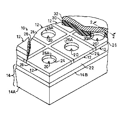
Fig. 1 is a fragmentary enlarged perspective
view of an array of field emission tubes showing the
snode and insulator that sep~rates the anode fro~ the
gate broken a~ay for clarity;
Fig. 2 is an enlarged sectional view taken
along line 2-2 of Fig. 1,
Figs. 3 and 4 are graphs showing probability
of collision of electrons in various gases versus
electron velocity (which is proportional to~v~liage),
Fig. 5 is a fragmentary enlarged perspective
~iew whlch is similar to that of Fig. 1 but showing an
array of field emission diodes instead of triodes, and
Fig. 6 is an enlarged sectional view taken
along line 6-6 of Fig. 5.
Reference first is made to Fig. 1 wherein an
arrsy 10 of microelectronic devices 12 is shown formed
on a substrate 14. In Fig. 1 the devices are shown to
comprise triode type "vacuum" tubes. As will become
apparent, diodes, tetrodes and other types of tubes may
be constructed in accordance with the present invention,
which de~ices function as vacuum tubes yet contain a
gas. Also, by way of example and not by way of
limitation, up to 2 x 10⁸ devices/cm2 may be formed on
sub~tra~e 14. From the ~bove, it will be apparent that
the devices are depicted on a greatly enlarged scale in
the drawings.
The ~ubstrate 14 provides a support for the
array 10 of tubes 12 formed ~hereon. In the illustrated
arrangement, substrate 14 comprises a base member 14A
`P
. .
. . . :
: : . ~ . . :
. . .: ~ . - .
. . . .
~X~39~6
together with a silicon layer 14B deposited thereon.
Base member 14A may be made of ceramic, glass, metal, or
like material, and for purposes of illustration a glass
member is shown. Silicon layer 14A is adapted for use
~n forming leads for cathodes 20 formed thereon. An
array of individual cathodes 20 is formed on silicon
layer 14B, each of which comprises a single needle-like
electron emittin8 protuberance. Protuberances 20 may
be formed of a refrsctory metal such as m~lybdenum or
tunpsten.
A dielectric film 22, such as a film of
silicon dioxide, is deposi~ed o~er the surface of
Qilicon layer 14B, which film is provided with an array
of apertures 24 through which the emitter electrode
protuberances 20 extend. Gate, or aceelerator,
electrodes 26 sre formed as by depo~iting a ~etal layer
on ~he dielectric film 22. For purposes of illustration,
crossing rows and ltne~ 28 of insulating material are
shown divid~ng film 26 into an array of indiYidual gate
electrodes. Gate electrodes 26 are the equivslent of
control gridx of conventional vacuum tubes. The upper
tips of the cathode protuberances terminate at a level
intermediate the upper snd lower surfaees of gate
electrodes 26 at substantially the center of ~perture
26~ in the electsodes for maximizing the electric field
at the tips undes tube operating conditions
-An insulating layer 30 is deposited on the
pate electrcdes 26, which layer is formed with
~~pertures 30A that are sxially ali~ned with apertures
: 30 2SA in the gate electrodes. A metal ~node 32 is affixed
to the insulating layer 30 which , if desired, may
comprise an unpatterned plane metal shee~ which requires
no alignment when pressed over the insulating surface.
A gas-contslning ~pace i~ formed between the snode 32
; 35 and lay~r 14B upon which the cathode protuberances 20
:~ : :
:: :
~ '
~ .
5 128~9~6
are formed. Unlike prior art arrangements wherein a
vacuum is provided, tubes of the presen~ invention
include a gas st a pressure of between approxima~ely
1/100 ~o 1 atmosphere in the interelectrode space.
Methods of produeing tubes of ~his type are
well kno~n ~s shown and described, for example, in ~he
above~mentioned U.5. Patent Number 3,789,471. With
cusre~t fabrica~ion methods, dimensions as small as H =
1.5 ~m, t ~ 0.5 ~m and r ~ 0.6 ~m may be achieved where
H is the thickness of ins~latin~ layer 22, t is the
thickness of the gate electrode 26 and r is the radius
of aperture 26A in the gate electrode, as identified in
Fig. 2. Also, a distance D of approximately 0.5 ~m
between the tip of cathode 20 and the anode 32 is
contemplated through use of an insulating layer 30 with
thickness on the order of 0.25 ~m.
PRINCIPLES OF OPE~ TION
It is know~ that the mean free path A of an
electron ln a gas traveling at velocity v (corresponding
to a potential V) is given by
T cm, (l)
273PPC ( V )
where:
p pressure ln ~orr,
T ~ ~bsolute ~emperature, and
Pc(V) ~ probability of collision for an electron of
: energy eV.
: Rearran8in8 equation ~1) provides an
expression for probability of collision as follows:
: . - ........ ~ , , ,
,
. " " . ". ~ ' ', ' ' ' ' , ' ............... ' . . .
~ '; ~ ' . , ' ~ . . ' ' ' , '
-
3L~839~L6
P~(V) = T (2)
273p A
Using equ2tion (2) and assuming that:
T ~ 300K,
p ~ 760 torr = one atmosphere, and
,~ > 0.5 ~,~m,
then Pc(V) would ha~e to be <30 for a tube with the
above-mentloned D ~ 0.5 ,~m dimension to operate
substantlally without colllsion of electrons with gas
contained therewithin.
iO Probability of collision, Pc~ is a function
of ~he electron velocity (or ~ ~oltage), and thi~
function has been measured for many gases. Functions of
probability of collision versus ~ vol~age for H2, Ne,
and He are shown in Fig. 3, and for N2 and 2 (the maJor
constituents of air) are shown in Fi8. 4. It will be
noted that often Pc has a maximum in the range of 2-10
~olts as a re~ult of the Bamsauer effect. If air is
employed in the tubes, operating Yoltages would have to
be away from the nitrogen peak which occurs at
~0 approximately 2.6 ~olts. As seen in Fig. 4, the
probability of collision for both nitrogen and oxygen
gases exc~ed 30 over a substantial portion of the
voltage range, thereby precluding operation within said
voltage range. HoweYer, by reduclng the pressurç of air
~N2 and 2) within the tube, the probability of
collision may be reduced to an acceptable Yalue, For
e~ample9 operation at 0.5 atmosphere air pressure
reduces the probability of collision to an acceptable
value a~ all operating voltages away f rom the nitrogen
peak.
From aD examination of Fig. 3, i~ will be seen
that for both neon and helium, the probability of
collision, Pc~ i8 less than 20 for all electron
. ~ - .
- - - . ,,
- , . .
., .......... , . ~ . : ~ . , ,
339~6
energies. Consequently, neon and helium at atmospheric
pressure may be employed in ~he tubes. They are
excellent gases to use because they are non-reactive and
inexpensive. For hellum, the minimum electron en~rgy
for ionlzation is 24.6 eV. Also, helium pene~rates most
materisls very easily, and if necessary can be used to
displace the air in the tube volume.
U~ing the sbove-mentioned dimensions (i.e.
r ~ 0.6 ~m, ~ - 1.5 ~m and t = 0.5 ~m) a gate voltage
of about +40V (relati~P to the cathode) is required to
extract 1 to 10 ~A from the cathode tip. With the anode
32 ~paced 0.5 ~um from the tip, an anode voltage of
about 75 to lOOV is required to ensure that no electrons
return to the gate. Extrapolation of existing
experime~tal data indicates that by reducing r to
0.3 ~m, it should be possible to reduce the gate
~oltage to ~ 5V and hence operate st sn anode voltage
of 10 to 20V~ With the illustrated construction wherein
the array of tubes is provided with a common anode,
operation of the tubes at a constant anode voltage is
provided. A vsriable gate vol~age is provided for
switching the tube between on and off condition~ in the
case the tubes are u~ed in, ~ay, a binary circult such
as a memory circult. The tube output may be obtained
from across a load resistor 36 connected between the
cathod~ 20 and ground.
With the present invention the tubes function
a~ vscuum tubes even though they contain gas at a
pressure of between l/100 atmosphere to 1 atmosphere.
Thls re~ult from the fact that the construction and
opersting conditions are such that the mean free path of
electrons is equal to or 8reater than the spacing
between the cathode and anode between which the
electrons travel, which spacing in accordance with the
present in~ention is no 8rester than abou~ 0.5~ m.
. . .
. : . . . . .
: , - . , . - -: . - ,
,,
~ - ~ : , :: :: -:
. . ,. .~ ~ . . .
9~6
With the present construction, th~ assembly
step that includes provlding a gas in the interelectrode
space is re3dily accomplished by simply performing
assembly in a ~aseous environment with the desired gas
and at the desired pressure. Gas pressures of, say,
between 1/100 and 1 a~mosphere are readily produced and
easily maintained during the assembly step at which gas
is sealed within the tubes. F~r example, in the
illustrated construction9 the anode 32 may be applied
within the desired gaseous e~vironment, say, within an
en~ironment of helium at substaDtially atmospheric
pressure. Upon bonding the anode 32 to the insulating
lsyer 30, the ineerelectrode space is sealed thereby
containing the gas within the tubes. No deep ~acuum
1~ pumping of the ~ubes is required to provide for an
operative arrsy of tubes.
Advantages of the novel triode tubes of this
invention include the fast switching speed compared,
say, to silicon3 gallium arsenide, and indium phosphorus
devices. Reference is made to Table 1 showing maximum
drift velocity, field strength, transit time for a
distance of 0.5 ~ m9 and applied voltage across 0.5 ,~m
of the above-mentioned metia and for a vacuum. In the
table the maximum ~alues of drift velocities of
electrons in the semiconductors Si, GaAs and InP sre
employed, which drift ~elocities are obtained from
graphs of dri~t Yelocity of electrons as a function of
electric field for the semiconductors. Because the tip
of cathode 20 is only about 0.05 ~m in diame~er (usin~
prior art construction methods) and because most of the
acceleration occurs w ie hi n 0.15 ~lm of the tip, it is
assumed that the in~erelectrode distance is travelled at
an essentially uniform ~elocity given by
.
'
'.
- ,. .
39~6
.
V 3 \~ (3)
TABLE 1
Medium Silicon GaAs InP Vacuu~
Msximum
5 Velocity (m/s) 10~2x10⁵ 2.2x10⁵ 6x10⁵V~
Obtained W$th
A Field of (V/m) 6X1060.8x106 2X10⁶ 3.2x10⁷
_ _ _ _ _ _ .
Transit Time (s) ~-
For 5x10-12 2.5x10-l2 2.27X1o-12 2.1x10⁻¹³
10 D ~ 0.5 ~m .:
Appli~d Voltage
Across 0.5 ~m 3 0.4 1 16
(volts)
*Field Limited By Breakdown across the insulator at
15 about 5x10⁷ V/ m.
-
:~ From Table 1 it will be seen that the "vacuum " tubes of
. this inveneion are capable of ~ switching speed about
;~ten times better than the best semiconductor now
:~Yailable.
: 20 : In order to detect whether current i6 flowing,the transport of~200 elcctrons is sufficient to have an
average error:sate of 1 in 1012, sssumin~ Poisson
~: ~ stati~tics. If the need is to detect whether a circuit
::
.
~ 39a~6
10
has current flowing in a time of 10-9 seconds~ then the
current flowin~ in the tube must be ;-
;~
200 x 1 6 x ~ 19 ~ 3.2 x 10⁻⁸ A
10-9
Thus, although the fluctuations in the field emitter may
be gr~ater than Poisson, it reasonably ~ay be assumed
that an 'on' current of lG-6 A/tlp is more than adequate
for detecting current flow at gigabit rates. The power
dissipated by a pair of 'on' tubes with this current
flowing and 16V anode voltage will be 3.2 x 10⁻⁵ W.
With each microtube occupying about 2.5 x 10⁻⁹ cm2 of
surface area, it 1s possible to pack up to a density of
about 108 memory circuits/cm2.
Reference now is made to Figs. 5 and 6 wherein
an array 50 of microelectronic diodes is shown formed on
a ubstrate 52. For purposes of illustration only,
substrate 52 upon which the diode array is suppo~ted is
shown ~o comprise a base member 52A of ceramic, glass,
metal, or the like, snd a silioon layer 52B deposited
thereon. Alternating rows of conducting cathode
connectors 54 and insulating material 56 are deposited
on silicon lay~r 52B. A linear array of $ndividual
cathodes 60 is formed on each of the cathode connectors
54, each of which ca~hodes comprise a single needle-like
electron emitting protuberance. As with the above-
~5 described triode array, protuberances 60 ~8y be formed~f a refractory met~l such as molybdenum or Sungsten.
A dielectric fiIm 62 is deposited over the
surface~ of the cathode connectors 54 and adjacent
insul~ting ~sserial 56, which film is provided with an
rray of spertures 64 into which the emitter electrode
; protuberance~ 60 e~tend. The upper tips of the cathode
protuberances t~rminate a short distance d below the
upp~r surfsce of ih~ulating layer 62.
.:
.
~: '
~339~6
Rows of metal anode electrodes 66 are affixed
to the insulating layer 62, which anode electrodes
extend in a direction at right angles to the rows of
cathode connectors 54. A gas-containing space is
provided st each cathode 60 between the rows of anodes
and crossing rows of cathode ~onnectors, which space is
filled with gas st 8 preqsure of between approximately
1/100 and 1 atmospher~. A di~tance d on the order of
0.5 ~m is provided between the tip of cathode 60 and
10 anode 66. hs with the ~riode tube embodiment, the diode
array is operated a~ vol~ages wherein the mean f ree pa~h
of electrons tra~elling in the ~as between the cathode
snd anode electrodes is equal to or grea~er than the
spacing d between the tip of the cathode electrode and
the associated anode electrode. As with the above-
described triode tube array, gases including air, neon,
helium, or the like, may be e~ployed in the diode array
structure. ~s with the triodes, the diodes function as
~acuu~ tubes even thou~h they contaln gas at a pressure
of between 1/100 atmosphere to 1 atmosphere. Also, the
anode strips 66 may be affixed to the insulating layer
62 in a gaseous environment of the desired gas at the
desired pressure ~hereby the gas-containing space
between the diode cathode and anode, contains the gas
upon complet~on of attachment of the aDodes to layer 62.
There is no requirement to reduce the gas pressure in
the interelectrode space after assembly of the tubes.
The inventio~ having been described in detail
in accordsnce with requirements of the Patent Statutes,
variou~ changes and ~odifications will suggest
themselYes to those skilled in this art. For exsmple,
the trlode type tubes may be provided with a separate
anode, if desired, in which case connection of the
snodes to a positive voltage source (selative to the
cathode) through individual load resistors is possible.
.. . . : ~ ::
. . ~: . . . :
. . .
- ., ., . . . ,.. , :.. . ...
~ ~8394~
,
12
With this structure, the triode cathodes may be formed
on a conducting substrate which may be connected to a
common d-c supply source. Also~ it will be apparent
that gases other thsn air, neon, and helium may be
employed in the tubes. It is intended that the above
and other such changes and modifications shall fall
within the spirit and scope of the invention as defined
in the appended claims.
'~
,
: :
, ' ' ~ ' , , '
: -: .: - , ~, . .