Note: Descriptions are shown in the official language in which they were submitted.
467~
MOTOR ROTATION SERVO CONTROL APPARATUS
BACKGROUND OF TH~ INVENTION
This invention relates to an apparatus applicable
to video tape recorders and the like for providing
accurate servo control of motor rotation.
Motor speed servo control apparatus have been
employed for controlling the speed of rotation of motors
used to drive VTR drums. It is the current practice to
perform such motor speed control based upon a motor
speed signal having a series of FG pulses generated at a
frequency corresponding to the motor speed sensed by a
frequency generator or the like sensor operable in
connection with the motor. One of serious problems is
reproduced picture distortion caused by noise
superimposed on the motor speed signal when the drum or
the frequency generator is mounted in an erroneous
manner to cause drum rotation variances. Such noise
superimposed on the motor speed signal has a frequency,
for example, 30 hertz, corresponding to the frequency of
rotation of the drum.
In order to avoid such a problem, it is the current
practice to design the motor speed servo control
apparatus to have a characteristic reducing the gain at
a frequency around 30 hertz. However, such gain
reduction raises another problem in that the servo
control accuracy is influenced considerably by torque
variations.
Alternatively, it has been proposed to provide an
analog notch filter to attenuate the gain at a frequency
around 30 hertz. However, this proposal is not suitable
for applications to video tape recorders or the like
where the speed of rotation of the drum is changed to
accommodate different modes of operation of the
apparatus so that the frequency of the noise
4~7~
superimposed on the motor speed signal due to drum
rotation variances changes from 30 hertz. Therefore, it
is not appropriate to minim:Lze reproduced picture
distortion by employing a filter having a high Q at a
frequency around 30 Hz.
SUMMARY OF THE INVENTION
A main object of the invention is to provide a
simple motor rotation servo control apparatus which can
control motor rotation with high accuracy.
It is another object of the invention to employ a
comb filter circuit to attenuate noise resulting from
motor rotation variances.
It is still another object of the invention to
provide a motor rotation servo control apparatus which
can employ inexpensive components to effect accurate
motor rotation servo control so as to minimize wow and
flutter.
There is provided, in accordance with the
invention, an apparatus for controlling rotation of a
motor. The apparatus comprises a sensor for sensing an
actual condition of the motor rotation for generating a
motor rotation signal indicative of the sensed condition
of the motor rotation. The sensor is connected to a
signal processor for processing the motor rotation
signal to provide an error signal indicative of an error
between the sensed and target conditions. A means is
connected to the signal processor for extracting an AC
component from the error signal. A comb filter circuit
receives the extracted AC component and filters out from
it a motor rotation component, which may be superimposed
on the motor rotation signal at a frequency of rotation
of the motor and its higher harmonics. The apparatus
also includes an adder for adding the filtered out
signal fed from the comb filter circuit and the error
4ti7~
signal fed from the signal processor to provide a
control signal used to control the motor.
In another aspect of the invention, there is
provided an apparatus for controlling the rotation of a
motor. The apparatus comprises a sensor sensitive to a
condition associated with the motor's rotation for
generating a sensor signal corresponding to the sensed
condition. The sensor is connected to a signal
processor for processing the sensor signal to provide
successive digital error signals each having a
predetermined bit number representing an error between
the sensed motor rotation condition and a target motor
rotation condition. The apparatus also includes a
digital-to-analog converter having a predetermined
effective bit number for converting a digital signal
into a corresponding analog signal used to control the
motor rotation. A data modification circuit is
connected between the signal processor and the
digital-to-analog converter for dividing each of the 20 successive digital error signals into a first digital
signal having upper bit data having a bit number equal
to or less than that of the digital-to-analog converter
and a second digital signal having the remaining lower
bit data. The first digital signal is applied to the
digital-to-analog converter. The data modification
circuit includes means for adding the second digital
signal to the next one of the successive digital error
signals.
In still another aspect of the invention, there is
provided an apparatus for controlling rotation of a
motor. The apparatus comprises a sensor sensitive to
motor rotation speed and phase for generating speed and
phase signals indicative of the sensed motor rotation
speed and phase, respectively, a first signal processor
for processing the speed signal to provide successive
4~
--4--
digital speed error signals each having a predetermined
bit number representing a speed error bet-~een the sensed
motor rotation speed and a target motor rotation speed,
and a second signal processor for processing the phase
signal to provide successive digital phase error
signals, each having a predetermined bit number
representing a phase error between the sensed motor
rotation phase and a target motor rotation phase. The
second signal processor is connected to a data
modification circuit for dividing each of the successive
digital phase error signals into a first digital signal
having the upper bit data and a second digital signal
having the remaining lower bit data. The data
modification circuit includes means for adding the
second digital signal to the next one of the successive
digital error signals. The apparatus also includes an
adder circuit for adding the digital speed error signal
fed thereto from the first signal processor and the
first digital signal fed from the data modification
circuit, a gate control circuit for multiplying the
digital speed error signal to the adder circuit by a
first value and multiplying the first digital signal to
the adder circuit by a second value greater than the
first value, and a digital-to-analog converter for
converting a digital signal fed from the adder circuit
into a corresponding analog signal used to control the
motor rotation.
BRIEF DESCRIPTION OF THE DRAWINGS
This invention will be described in greater detail
by reference to the following description taken in
connection with the accompanying drawings, in which like
numerals identify like elements in the several figures
and in which:
1~4~
Fig. 1 is a schematic block diagram of a comb
filter circuit applicable to the invention;
Fig. 2 contains two wave.orms used in explaining
the manner in which speed error data are formed;
Fig. 3 contains four waveforms obtained at various
points of the comb filter circuit;
Fig. 4 is a graph showing the gain versus frequency
characteristic of the comb filter circuit;
Fig. 5 is a schematic block diagram showing one
embodiment of a motor rotation control apparatus made in
accordance with the invention;
Fig. 6 contains three waveforms used in explaining
the manner in which phase error data are formed;
Fig. 7 is a schematic block diagram showing a
second embodiment of the motor rotation control
apparatus of the invention;
Fig. 8 is a diagram used in explaining the manner
in which speed and phase error data are added before
application to a digital-to-analog converter;
Fig. 9 is a schematic block diagram showing a
modified form of the motor rotation control apparatus of
the invention;
Fig. lO is a schematic block diagram showing a
third embodiment of the motor rotation control apparatus
of the invention; and
Fig. 11 is a schematic block diagram of a comb
filter circuit applicable to the third embodiment of the
motor rotation control apparatus.
DETAILED DESCRIPTION OF THE INVENTION
Prior to the description of the preferred
embodiment of the present invention, a description will
be given of a comb filter circuit which is used in the
motor rotation control apparatus of the invention for
removal of a component OL DC and a 30 ~z component and
its higher harmonics from a signal inputted thereto.
Referring to Fig. 1, the comb filter circuit,
generally designated by the numeral 10, has an input
terminal 12 and an output terminal 14. The input
terminal 12 is connected to one input of an adder 16
which has an output connected to the output terminal 14.
The input terminal 12 is also connected to the wiper of
a six position switch 22 whose six contacts 22a ... 22f
are connected through respective digital primary low
pass filters 30A ... 30F to corresponding fixed contacts
24a ... 24f of a six position switch 24 whose wiper is
connected to another input of the subtracter 16.
Although only contacts 22a, 22b, and 22f, filters 30A,
30B, and 30F, and contacts 24a, 24b, and 24f have been
shown for purposes of clarity, it will be understood
that these other elements, corresponding to those which
are shown, are in the actual embodiment.
The digital primary low pass filter 30A includes a
subtracter 32 having an input connected to the fixed
contact 22a. The output of the subtracter 32 is coupled
to an integrator comprised of an adder 34, a limiter 36
and a delay circuit 38. The adder 34 receives an input
from the subtracter 32 and has an output connected
through the limiter 36 to the delay circuit 38. The
output of the delay circuit 38 is connected to another
input of the adder 34 and also to a multiplier 40 having
a multiplication factor K smaller than unity. The
output of the multiplier 40 is coupled to the fixed
contact 24a. The other digital primary low pass filters
30B ... 30F are substantially the same in structure as
the primary low pass filter 3OA.
Referring to Fig. 2, the waveform (a) represents a
series of FG pulses generated at a frequency
cor-es_ondins to a drum motor spee~ sensed by 2 sensor.
1~4~7~
These FG pulses are used to control a counter in such a
manner that the counter clears its counter and starts
counting clock pulses at the leading edge of each of the
FG pulses and its count is sampled at the trailing edge
of the FG pulse as shown by the waveform (b) of Fig. 2.
The sampled values N1, N2, N3 ... constitute speed error
data DS which are used to rotate the motor at a constant
speed. If errors occur upon mounting the drum or the
sensor, however, a 30 Hz component and its higher
harmonics which are multiples of the DC component and
the 30 Hz component may be superimposed on the speed
error data DC, causing picture distortion. The filter
circuit 10 can remove the 30 Hz component and its higher
harmonics from the speed error data DS in the following
manner:
Assume that the comb filter circuit 10 receives, at
its input terminal 12, speed error data DS including the
sampled values N1, N2, N3 ..., as shown by the waveform
(a) of Fig. 3. The switches 22 and 24 receive the
sampling signal from the counter and are thus switched
in synchronism with the times at which the counter
counts Nl, N2, ... are sampled in such a manner that the
comb filter 30A can handle sampled counts N1, N7, N13,
..., a primary low pass filter 30B (not shown) can
handle sampled counts N2, N8, N14, ..., a primary low
pass filter 30C (not shown) can handle sampled counts
N3, N9, N15, ..., a primary low pass filter 30D (not
shown) can handle N4, N10, N16, ..., a primary low pass
filter 30E (not shown) can handle sampled counts N5,
N11, N17, ... , and the primary low pass filter 30F can
handle sampled counts N6, N12, N18, ... .
When each of the counts Nl, N7, N13, ... is
sampled, the switch 22 is set to connect the input
terminal 12 to the primary low pass filter 30A and the
switch 24 is set to connect the primary low pass filter
7~
3OA to the adder 15. As a result, the speed error data
DS1, as shown by the waveform (b) OL Fig. 3, are fed to
the primary low pass filter 30A. The data DS1 are fed
to the subtracter 32 and hence to the integrator
comprlsed of the adder 34, the limiter, 36 and the delay
circuit 38. The limiter 36 limits the dynamic range of
the signal inputted thereto. The delay circuit 38
delays the signal inputted thereto for a time during
which six counter counts are sampled; that is, the drum
motor makes a full rotation. The delay circuit 38
generates data DS2 which are fed back to the adder 34
where they are added to the next data fed thereto from
the subtracter 32. For example, if the data DS2
corresponds to the sampled count Nl, the adder 34 adds
the data DS2 to the data corresponding to the count N7
sampled in the following sampling cycle. The data DS2
represent the average value of the data DSl. The data
DS2 are fed to the multiplier 40 where the data DS2 are
multiplied by the multiplication factor K smaller than
unity to develop data DS3. The data DS3 represent an
error of each of the sampled counts N1, N2, N3, ... from
a center value (zero level), as shown by the waveform
(c) of Fig. 3. It means that the primary low pass
filter 30A functions in a manner substantially
equivalent to an RC low pass filter for analog signals.
The data DS3 are fed back to the subtracter 32 which
subtracts the data DS3 from the data DSl. The data DS3
are fed from the multiplier 40 to the subtracter 16
which subtracts the data DS3 from the data DSl.
In a similar manner, the switches 22 and 24 are set
to operate the other primary low pass filters 3OB
30F successively. The result is that the subtracter 16
receives data DS4 which represent the 30 Hz component
and its higher harmonics extracted from the data DS.
The ~dder 16 subtracts the data DS4 f-Gm thC origina
1~4~
data DS to remove the 30 ~z component and its higher
harmonics rrom the data DS. The data DS developed at
the output terminal la is shown by the waveform (d) of
Fig. 3. Fig. 4 shows the gain versus frequency
characteristic of the comb filter circuit 10. It is to
be noted that the frequencies of 30 Hz, 60 Hz and 90 Hz
correspond to the drum motor rotational frequencies
selected respectively in various modes of operation of
the video tape record/playback apparatus. Therefore,
the comb filter circuit 10 is effective to remove noise
components superimposed on the speed error data due to
nonuniform motor rotation at any selected motor speed.
Normally, the input data DS has a DC component
which represents a reference value for motor speed.
Since the DC component remains on the data DS4, the
subtracter 16 removes the DC component when it subtracts
the data DS4 from the data DS. This means that the comb
filter circuit 10 cannot transmit a DC component. In
order to transmit such a DC component, the comb filter
circuit 10 is required to operate with a very complex
and expensive circuit which can calculate the average
value of the outputs of the respective comb filters 30A
... 30F or the average value of the input data DS and
subtract the calculated average value from the data DS4.
The invention provides a motor rotation control
apparatus which employs a simple circuit associated with
such a filter circuit as shown in Fig. 1 to permit DC
component transmission.
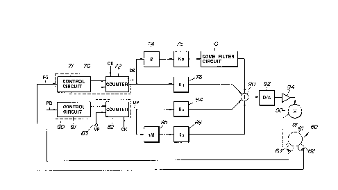
Referring to Fig. 5, there is illustrated one
embodiment of a motor rotation control apparatus made in
accordance with the invention. The apparatus is shown
as including speed-servo and phase-servo loops for
controlling rotation of a drum motor 50 in a manner to
rotate a drum (not shown) at a constant speed. The
apparatus includes a motor ~ota=ion sensor ~0 having a
1~4~i7~
--10--
frequency generator G- pulse generator 61 operable in
connection with the drum mo~or 50 and first and second
heads 62 and 63 disposed in close proximity to the
circumference of the generator 61 for generating signals
which indicate the speed and phase of rotation of the
drum motor 50. The first head 62 develops a series of
FG pulses at a frequency corresponding to the speed of
the drum motor 50, as shown by the waveform (a) of
Fig. 2. The second head 63 develops a series of PG
pulses each corresponding to 360 degrees of rotation of
the drum motor 50, as shown by the waveform (b) of
Fig. 6. The FG pulses are fed from the first head 62 to
a speed error data forming circuit 70 which forms a part
of the speed servo loop. The PG pulses are fed from the
lS second head 63 to a phase error data forming circuit 80
which forms a part of the phase servo loop.
The speed error data forming circuit 70 is shown in
schematic form as including a control circuit 71
connected to control a counter 72. The control circuit
71 develops a reset/start (RSC) command signal at the
leading edge of each of the FG pulses and a sample (SC)
command signal at the trailing edge of each of the FG
pulses. Upon occurrence of such a reset/start (RSC)
command signal, the counter 72 clears its count and
starts counting clock pulses CK generated at a
predetermined frequency, for example, 1 megahertz. The
sample (SC) command signal is applied to sample the
count N of the counter 72. The speed error data forming
circuit 70 produces speed error data DS which include
the count values N1, N2, N3, ... that are sampled in a
sequential fashion, as shown in Fig. 2(b).
The output of the speed error data forming circuit
70 is coupled to an adder circuit 90 through a series
circuit of a differentiating circuit 74, a first
multiplier circuit 75 and the fllter circui_ 10 and also
4~j7~
~ 1
throush a second mul,iplier circlit 76. The
differentiating circui. 74 differentiates the speed
error data DS .o conver. .hem into angular acceleration
error data. It is to be noted that the DC component of
the speed error data DS is removed while it is
differentiated in the differentiating circuit 74 and the
angular acceleration error data have an AC component
only with no DC component. The first multiplier 75 has
a predetermined first multiplication factor K and
multiplies the angular acceleration error data by the
first multiplication factor to provide a weight for the
data communicated therethrough. The multiplied angular
acceleration error data are fed from the first
multiplier circuit 75 to the filter circuit 10. The
filter circuit 10 removes the 30 Hz component and its
higher harmonics which may be superimposed on the
received data, in the same manner as described
previously in connection with Fig. 1. The second
multiplier circuit 76 has a predetermined second
multiplication factor Kl and multiplies the speed error
data DS by the second multiplication factor Kl to
provide a weight for the data communicated therethrough.
This loop including the second multiplier 76 is
effective to communicate a DC component which represents
a target or reference motor speed required to control
the drum motor 50.
The phase error data forming circuit 80 is shown in
schematic form as including a control circuit 81
connected to control a counter 82. The control circuit
81 develops a sample (SC) command signal at the leading
edge of each of the PG pulses fed thereto from the
second head 63. A vertical synchronization signal VP,
shown in Fig. 6 (a), is applied at a terminal 83 to
cause the counter 82 to clear its count and start
countlng clock pulses CK gener2ted a. a predetermined
4~
-12-
fre~uency, Sor example, 1 me~ahertz. The sample (SC)
command signal is applied Lrom the control circuit 81 to
sample the count M of the counter 82. The phase error
data forming circuit 80 produces phase error data DP
which include the count values M1, M2, ... that are
sampled in a sequential fashion, as shown in Fig. 3.
The output of the phase error data forming circuit
80 is coupled to the adder so through a third multiplier
circuit 84 and also through a series circuit of an
integration circuit 85 and a fourth multiplier circuit
86. The third multiplier circuit 84 has a predetermined
third multiplication factor K2 and multiplies the phase
error data DP by the third multiplication factor K2 to
provide a weight for the data communicated therethrough.
The integration circuit 85 integrates the phase error
data DP. The fourth multiplier circuit 86 has a
predetermined fourth multiplication factor K3 and
multiplies the integrated data by the fourth
multiplication factor K3 to increase the gain of the
phase servo loop for low-frequency band components.
The adder 90 adds the data fed from the filter
circuit 10 and the second, third and fourth multiplier
circuits 76, 84 and 86. The added data are fed from the
adder 90 to a digital-to-analog converter 92 which
converts them into a corresponding analog control
signal. This control signal is applied to a drive
amplifier circuit 94 which thereby controls the speed
and phase of rotation of the drum motor 50.
In the illustrated embodiment, the first, second,
third and fourth multiplication factors K, K1, K2 and
Ka are set as K > Kl > KZ ~ K3 in order that the motor
rotation control apparatus has a faster response to a
speed error than is obtained for a phase error.
In the illustrated embodiment, the speed error data
DS are d~- e _ntiate~ to have their DC component removed
4~
-13-
be_ore the data are processed in the fllter circuit 10
so that the filter circult 10 can handle the AC
component only. This permits the rotation control
apparatus to remove only the component related to the
actual variances of rotation o~ the drive motor 50.
This effect is improved by the first multiplier circuit
75, which has the greatest multiplication factor K. In
addition, the DC component produced by a hold means in
the counter 72, which represents a target or reference
motor speed required to control the drum motor, is
communicated through the second multiplier circuit 76 to
the adder 90.
Although this embodiment has been described in
connection with a digital servo circuit, it is to be
noted that it is equally applicable to analog servo
circuits, in which case the delay circuit 38 (Fig. 1)
may use a CCD (charge coupled device) element.
According to this embodiment, it is possible to
remove errors introduced into motor rotation servo
control due to motor rotation variances by a simple
circuit arrangement. In addition, it is possible to
handle superimposed noise and its higher harmonics by
only using comb filters having a high Q. This is
effective to avoid low-frequency band phase shift and to
achieve stable and accurate motor rotation control.
Referring to Fig. 7, there is illustrated a second
embodiment of the motor rotation control apparatus of
the invention. The apparatus is shown as including
speed-servo and phase-servo loops for controlling
rotation of a drum motor 150 in a manner to rotate a
drum (not shown) at a constant speed. The apparatus
includes a motor rotation sensor 160 which includes a
frequency generator or pulse generator 161 operable in
connection with the drum motor 150, and first and second
heads 162 and 153 dispose~ -~ cl OS2 roximity _o the
1 ~4~
circum~erence oî the generato~ 161 for generating
signals which indicate the speed and phase of rotation
of the ~rum motor 150. The ~^irst head 152 develops a
series of FG pulses at a frequency corresponding to the
speed of the drum motor 150, for example, three pulses
for one rotation of the drum motor 150, as shown by the
waveform (a) of Fig. 2. The second head 163 develops a
series of PG pulses each corresponding to 360 degrees of
rotation of the drum motor 150, as shown by the waveform
(b) of Fig. 6. The FG pulses are fed from the first
head 162 to a speed error data forming circuit 170 which
forms a part of the speed servo loop. The PG pulses are
fed from the second head 163 to a phase error data
forming circuit 180 which forms a part of the phase
servo loop.
The speed error forming circuit 170 is shown in
schematic form as including a control circuit 171
connected to control a speed error counter 172. The
control circuit 171 develops a reset/start (RSC) command
signal at the leading edge of each of the FG pulses and
a sample (SC) command signal at the trailing edge of
each of the FG pulses. Upon occurrence of such a
reset/start (RSC) command signal, the speed error
counter 172 clears its count and starts counting clock
pulses CK generated at a predetermined frequency, for
example, 1 megahertz. The sample (SC) command signal is
applied to sample the count N of the speed error counter
172. The speed error data forming circuit 170 produces
speed error data DS which include the count values Nl,
N2, N3, ... that are sampled in a sequential fashion, as
shown in Fig. 2(b).
The output of the speed error data forming circuit
170 is coupled to an adder 200 through a first gain
control circuit 174 which may be in the form of a
mul iplier circuit having 2 --ede'~ ned mult plication
~X~4~i7;~:
.^ac_or X4. The first gain control circuit 17~
multiplies the speed error data DS by the multiplica~ion
factor K4 to provide a weight for the data communicated
therethrough.
The phase error data forming circuit 180 is shown
in schematic form as including a control circuit 181
connected to control a phase error counter 182. The
control circuit 181 develops a sample (se) command
signal at the leading edge of each of the PG pulses fed
thereto from the second head 163. A vertical
synehronization signal VP is applied at a terminal 183
to cause the phase error counter 182 to clear its count
and start eounting eloek pulses CK generated at a
predetermined frequeney, for example, 1 megahertz. The
sample (SC) command signal is applied from the eontrol
eireuit 181 to sample the eount M of the phase error
eounter 182. The phase error data forming cireuit 180
produees phase error data DP whieh inelude the eount
values Ml, M2, ... that are sampled in a sequential
fashion, as shown in Fig. 3.
The output of the phase error data forming eireuit
180 is eoupled through a data modifieation cireuit,
designated generally as 190, to a seeond gain eontrol
eireuit 198 and henee to the adder 200. The seeond gain
eontrol eireuit 198 may be in the form of a multiplier
eireuit having a predetermined multiplication faetor Ks
to provide a weight for the data eommunieated
therethrough. A eomputer 210 eontrols the gains K4
and Ks~ but does not seleet these faetors.
The data modifieation eireuit 190 ineludes an adder
191 having an input from the phase error data forming
eireuit 180. The adder 191 has an output conneeted to
one input of an AND gate 192 having another input
eonneeted to a terminal 193 to whieh a signal having an
FOH eode represented as "11110000" is applied. The
4~
-~5-
output OI the adde- 191 is also connec~ed to one input
o, a subtracter 194 which has another input connected to
the output of the ÆND gate 192. The output of the
subtracter 194 is connected through a delay circuit 195
to another input of the adder 191. The output of the
AND gate 192 is connected to the second gain control
circuit 198.
The adder 200 adds the data fed from the first and
second gain control circuits 174 and 198. The added
data are fed from the adder 200 to a digital-to-analog
converter 202 which converts them into a corresponding
analog control signal. This control signal is applied
to a drive amplifier circuit 204 which thereby controls
the speed and phase of the drum motor 150.
The operation of the data modification circuit l9o
will be described. First of all, for purposes of this
explanation, assume that the output of the phase error
data forming circuit 180 is connected directly to the
second gate control circuit 198 with the data
modification circuit 190 being removed. The first gate
control circuit 174 multiplies the speed error data DS
by the multiplication factor K4 and produces data
represented as K4 x DS. The second gate control circuit
198, multiplies the phase error data DP by the
multiplication factor K5 and produces data represented
as Ks x DP. The adder 200 adds the data K4 x DS and the
data K5 x DP. Assuming now that both the speed error
data DS and the phase error data DP are eight bit data
and that the multiplication factor K4 is set at about 1
and the multiplication factor Ks is set at 2 4, the data
outputted from the adder 200 is represented as:
K4 x DS + Ks x DP = DS + 2 x DP
-17-
As shown in Fig. 8, the data 2 4 x DP are
equivalent to the phase error data DP shifted four bits
toward the lower bit side and, thus, the added data DS '
2 4 x DP are 12 bit data. The added data are fed to the
digital-to-analog converter 202. It is preferable that
the digital-to-analog converter 202 is an eight bit
converter in view of cost considerations. Such an
eight-bit digital-to-analog converter converts the upper
eight-bits of digital data into analog form while
omitting the other lower four-bits of data. However,
this manner introduces noise into the control signal so
as to degrade the motor rotation control accuracy,
increase wow and flutter, and exert adverse influences
on the signal particularly in its low frequency band.
Although it may be possible to overcome the problem by
employing a 13 bit digital-to-analog converter, it is
too costly to be used in such an apparatus.
The data modification circuit 190 provides an
elegant solution to the above problems. The AND gate
192 is open to communicate the data from the adder 191
to the second gain control circuit 198 when it receives
a logic 1 level signal at the other input to which the
FOH code signal "11110000" is applied. Therefore, the
AND gate 192 communicates the upper four-bits of data of
the eight-bit phase error data DP to the second gain
control circuit 198 and also to the subtracter 194 which
subtracts the upper four-bits of data from the eight-bit
phase error data DP fed thereto from the adder 191. As
a result, the subtracter 194 develops a signal
representing the lower four-bits of data. The lower
four-bits of data are fed to the delay circuit 195 which
provides a predetermined time delay relative to the
signal applied thereto from the subtracter 194, the
predetermined time delay corresponding to one sampling
35 interval z_ whlch the co~nt values Ml, M2, are
4~i7;~
sampled, 2s shown in ~-ig. 6(c). ~he delay circuit 195
may employ a memory, an eight-bit shift register, or the
li~e czpable of celaying the lower rour-bits of data for
a time corresponding to the time interval-at which the
count values M1, M2, ... are sampled, as shown in Fig.
6(c). The adder 191 adds the lower four-bits of data of
the previously sampled phase error data DP to the lower
four-bits of data of the presently sampled phase error
data DP in such a manner that 1 is added to the digit at
the fourth bit position from the most significant bit
(MSB) of the phase error data DP. The added data are
fed through the subtracter 194 and the delay circuit 195
to the adder 191 again. This operation is repeated so
that the adder 191 accumulates the lower four-bits of
data.
When the lower four-bits of data are accumulated, 1
is added to the digit at the fourth bit position from
the most significant bit (MSB) of the phase error data
DP; that is, at the lowermost bit position of the upper
four-bits of data obtained from the AND gate 192. The
upper four-bits of data are fed to the second gain
control circuit 198.
Referring to Fig. 9, there is illustrated a
modified form of the data modification circuit applied
for more general purposes. This modification is
effective to compensate for the lower bits of data of a-
bit error data inputted to the data modification
circuit, the upper bits of data being fed to a digital-
to-analog converter 300 having an effective bit number _
smaller than the bit number a of the error data.
In Fig. 9, the data modification circuit, generally
designated by the numeral 290, includes an adder 291
having an input at which a-bit data D are fed. The
adder 291 has an output connected to one input of an AND
gate 292 havina -r.other input connec~ed to a terminal
--19--
293 to ~hich a signal having a code is applled for
ex,rac~ing the upper bits of (b-bit) data from the
inputted a-bi, data D. The output of the adder 251 is
also connected to one in?ut of a subtracter 294 which
has another input connected to the output of the AND
gate 292. The output OI the subtracter 294 is connected
through a delay circuit 295 to another input of the
adder 291. The output of the AND gate 292 is connected
to the digital-to-analog converter 300 which converts a
k-bit digital signal into a corresponding analog signal
which is used to control a motor 150.
The AND gate 292 is open to communicate the data
from the adder 291 to the digital-to-analog converter
300 when it receives a logic 1 level signal at the other
input 293 to which the code signal S is applied.
Therefore, the AND gate 292 communicates the upper k-bit
data of the a-bit data D to the digital-to-analog
circuit 300 and also to the subtracter 294 which
subtracts the upper b-bit data from the a-bit data D fed
thereto from the adder 291. As a result, the subtracter
294 develops a signal representing the lower c (a-k) bit
data. The lower -bit data are fed to the delay circuit
295, which provides a predetermined time delay relative
to the signal applied thereto from the subtracter 294,
the predetermined time delay corresponding to one
sampling interval at which the data D is formed. The
delay circuit 295 may employ a memory, a shift register,
or the like capable of delaying the lower c-bit data a
time corresponding to the one sampling time. The adder
291 adds the lower c-bit data of the previously sampled
data D to the lower c-bit data of the presently sampled
data D in a similar manner as described in connection
with Fig. 7. The added data are fed through the
subtracter 294 and the delay circuit 295 to the adder
291 again. Thls ope~a~lon ls repea,ed so tha_ ~he 2dde~
4~i7~
-20-
291 accumula~es ~ e lower c-bit data. ~*.en the lcwe~ ~-
bit data are ac-umulated, 1 is added to the digit at the
lower~os' bi_ position of the upper k-bit data. The
upper _-bit data are fed to the digital-to-analog
converter 300 where they are converted into digital form
for controlling the motor 150. It is, therefore,
apparent that the apparatus is effective to improve the
motor rotation control accuracy.
Referring to Fig. 10, there is illustrated a third
embodiment of the servo control apparatus of the
invention which is substantially the same as the
embodiment shown and described in connection with Fig. 5
except for a data modulation circuit provided in each of
the circuits to the adder 90. Accordingly, parts in
Fig. 10 which are like those in Fig. 5 have been given
like reference numerals. Parts which are slightly
different in form have been given like reference
numerals with a prime suffix.
In this embodiment, a data modulation circuit 320
is provided on a line between the second multiplier
circuit 76 and the adder 90. The data modulation
circuit 320 is substantially the same as the data
modulation circuit 290 shown and described in connection
with Fig. 9 except for the code signal applied to the
other input 293 of the AND gate 292. The code signal
FCH, which is dependent on the multiplication factor K1,
is selected in a manner permitting the digital-to-analog
converter 92 to convert the input digital data into
analog form without omitting any part of the digital
data, as described in connection with Figs. 7 and 9.
For example, the code signal FCH may be "11111100" if
the multiplication factor Kl is 2-2. A data modulation
circuit 340 is provided on a line between the second
multiplier circuit 84 and the adder 90. The data
modulztion cir_uit 340 is subst~nti~lly the s2me 2S the
data modula,ion circui. 250 shown znd describe~ in
connection wi_h Fig. 9 except '~or ~he code slsnal
applied to the other input 293 o,~ the ~D gate 292. The
code signal F0H, which is dependent on the
multiplication factor K2, is selected in a ~anner
permitting the digital-to-analog converter 92 to convert
the input digital data into analog form without omitting
any part of the digital data, as described in connection
with Figs. 7 and 9. For example, the code signal F~H
may be "11110000" if the multiplication factor K2 is
2-4. A data modulation circuit 360 is provided on a
line between the second multiplier circuit 86 and the
adder 90. The data modulation circuit 360 is
substantially the same as the data modulation circuit
290 shown and described in connection with Fig. 9 except
for the code signal applied to the other input 293 of
the AND gate 292. The code signal C0H, which is
dependent on the multiplication factor K3, is selected
in a manner permitting the digital-to-analog converter
92 to convert the input digital data into analog form
without omitting any part of the digital data, as
described in connection with Figs. 7 and 9. For
example, the code signal F~H may be "11000000" if the
multiplication factor K3 is 2-6.
Referring to Fig. 11, the comb filter circuit lOa
is shown in detail. The comb filter circuit lOa is
substantially the same as the comb filter circuit 10
described in Fig. 1 except for a data modification
circuit 41 which is connected at the output of the
multiplier 40. The data modification circuit 41 is
substantially the same as the data modulation circuit
290 shown and described in connection with Fig. 9 except
for the code signal applied to the other input 293 of
the AND gate 292. The code signal, which is dependent
on the mult~?lication factor K, is se'eY.ed ~n a m2nne
4~j7~
pe~lttins .he digital-to-analog converter 92 to conve-t
.he input digital data into analog 'orm wlthout omitting
any part o. the digital data, as desc-ibed in connec~ion
with Figs 7 and 9
While the invention has been described in
conjunction with specific embodiments thereof, it is
evident that many alternatives, modifications and
variations will be apparent to those skilled in the art
Accordingly, it is intended to embrace all alternatives,
modifications and variations that fall within the scope
of the appended claims