Note: Descriptions are shown in the official language in which they were submitted.
~34~
--1--
Back~round of the Invention
_ _ __ _ _ _ __ _____ __
1. Field_of_the_Invention
The present invention relates to direct current linked,
alternating current inverter drives for induction motors
S and machines having similar load characteristics.
2. Descri~tion of the Prior Art
A discussion of the prior art will take place in
detail hereinbelow.
3. Summar~ of the Invention
In contrast to the prior art, the drive of the present
invention includes a six-step voltage source inverter with
capacitive loading on the output wherein the capacitive
energy storage capacity is only slightly less than the
inductive energy storage capacity of the motor. In prior
art inverter drives, such large capacitances would have
produced intolerable snubbering losses, but due to the
unique features of the drive of the present invention,
such losses are avoided.
There are several direct benefits of employing such
capacitive loading in the output stage in the drive of the
present invention. The rate of change of voltage across
the inverter switching elements is decreased significantly,
by as much as 100 to 1000 times, and is typically about
0.5 volts per microsecond for 230 volt A.C. drive. This
reduction in the rate of voltage change at the switching
element permits the use of less expensive switching devices
and simpler switching techniques. Furthermore, the drive
of the present invention does not require free-wheeling,
anti-parallel cliodes at the output stage, .since large
induction currents are absorbed in the capacitive bufEering
rather than being recirculated around the output switching
elements. This simplifies the output section of the
inverter drive and allows negative voltage operation of
the Outp-lt to produce negative torque. In the drive of
the present invention, full four-quadrant operation is
possible with only six switching elements or thyristors in
each input and output section.
--2--
In the drive of the present invention, it is not only
necessary that the switching frequency of each switching
element in the output stage be controlled to ef~ect motor
speed but also that the switching elements be enabled only
when the voltage across the switching device is less than
a prescribed amount, typically five volts. By thus
controlling the output switching elements, the drive of
the present invention prevents destructive current flow
into the bu~fering capacitors and greatly reduces the
changes of a short circuit in the output bridge which
might occur if opposite polarity elements in the output
bridge were enabled simultaneously.
In the drive according to the present invention,
simple switching elements capable of reverse voltage
blocking such as a transistor commutated thyristor
switching element may be used as the inverter switching
elements in the drive of the present invention.
The benefits provided by the motor drive of the present
invention include more efficient inversion, reduction of
switching losses, and elimination of snubber and forced
commutation losses. Furthermore, lower voltage tolerant
switching elements may be used in the output stage since
there are no transient over voltages caused by hi~h speed
switching. The drive of the present invention also
provides quieter inverter and motor operation by
eliminating current surges and more efficient, cooler
motor operation by minimizing the harmonic currents which
in conventional drives are absorbed in the motor as a
result Oe voltage 6Wi tching.
By eliminating the need for anti-parallel, free-
wheeling diodes, the drive of the present invention permits
the output switching elements, such as silicon controlled
rectifiers, to be reverse biased during COmmUtAtiOn.
Furthermore, the elimination of these free-wheeling diodes
also reduces the likelihood of line-to-ground short
circuits, and provides a drive which produces almost
constant current Elow into the output during all phases of
--3--
operation, full speed as well as low speed. When combined
with the characteristic constant voltage, this provides
near constant power and therefore very low torque pulsation
in the motor even at low frequencies. Since almost a
constant current flow exists in the drive, relatively small
filter capacitors may be used thereby reducing the cost of
the overall drive~
In accordance with an aspect of the invention there is
provided an alternating current, induction motor drive,
for providing alternating drive current from a direct
current voltage source, comprising a pluralit~ of gate
controlled motor drive switching elements forming a three-
phase motor drive inverter circuit, said inverter circuit
being connected between the voltage source and the motor;
switch control means for controlling said motor drive
switching elements in timed relation so as to provide the
three-phase drive current to the motor, said switch control
means including voltage sensing means for preventing said
;. switching elements from being actuated unless the voltage
across said switching elements is less than a prescribed
minimum value, said switch control means comprising: means
for force-commutating said switching elements; and gate
control means for selectively enabling said gate controlled
switching elements in a timed relation so as to provide
three-phase drive current to the motor; and a plurality of
capacitive buffering means having a first terminal and a
second terminal, said Eirst terminal being connected
between said switching elements in each phase of said
inverter circuit and said second terminal being connected
to said Eorce-commutation means, said capacitive buffering
means being selected to have an energy storage capacity
slightly less than the energy storage capacity of the
: motor.
DescrlE~ion of the Drawings
Fig. 1 is a schematic electric circuit diagram of a
conventional variable-voltage, variable-frequency square
wave induction motor drive;
18~8
--4--
Fig. 2 is a schematic electrical circuit diagram of a
conventional capacitive buffering or snubbering;
Fig. 3 is a schematic electric circuit diagram of an
inverter motor drive in accordance with the present
invention;
Figs. ~ and 5 are schematic electric circuit diagrams
oE portions of a motor drive according to the present
invention;
Fig. 6 is a schematic electric circuit diagram of a
portion of a motor drive according to the present
invention;
Figs. 7 and 8 are schematic electric circuit diagrams
of portions of a motor drive according to the present
invention;
Fig. 9 is a schematic electric circuit diagram of a
portion of a motor drive according to the present
invention;
Figs. 10 and 11 are schematic electric circuit diagrams
of portions of a motor drive according to the present
invention.
Descri~ n of the Preferred Embodiments
In the past, alternating current induction motor drive
circuits were generally either constant current drives,
wherein the inverter output section was provided with a
relatively constant direct current, or constant voltage
drives wherein the inverter output section was provided
with a relatively constant direct current voltage.
Adjustable speed voltage-fed drives t,ypically were either
variable voltage, variable Erequency square wave inverter
drives or more recently pulsed width modulation inverter
drives.
Pulsed width modulation drives included a constant
link voltage input to a pulse modulation circuit which
synthesized a variable voltage, variable frequency motor
drive output.
A typical, square wave, variable voltage, variable
~requency inverter drive is illustrated in Fig. 1. The
inverter drive illustrated in Fig. 1 does not include the
--5~
commu~ation circuitry required to force commutate the
output silicon controlled rectifiers or thyristors. In
these type of six-step inverter drives, each of the
inverter legs was enabled for 180 to provide an output
line-to-line voltage generally similar to the six-step
wave form illustrated schematically in Fig. 1.
In these square wave inverter type motor drives, the
speed of the motor was controlled by varying the inverter
commutation fre~uency. In order to maintain adequate
1~ torque capability it was necessary to also vary the DC
link voltage to maintain a constant ratio of voltage to
frequency. Hence, these types of drives were referred to
as variable ~oltage, variable fre~uency, inverter drives.
Inverter drives typically used gate controlled,
switched circuit elements such as thyristors or silicon
controlled rectifiers, which were enabled by providing a
gate bias voltage but which also required external forced
commutation circuitry to provide reverse bias voltage to
disable the switch. Alternatively, some inverter drives
used gate controlled switching elements such as
transistors, gate turn-off thyristors or insulated gate
transistors. In circuits with these type of switching
elements, current flow through the switch was interrupted
by applying, or removing, base-to-emitter bias voltaye.
In either case, the switching element was used to
interrupt current flow into the induction motor which
inherently produced rapid voltage changes across the
switching element, i.e., a high dV/dT.
Since most economically available switching elements
could not tolerate these rapid voltage changes, typical
inverter drives also included some capaci-tive buffering or
snubbering to protect the switching element. Snubbering
circuits, however, produced losses proportional to the
amount of protection afforded. In the conventional
snubbering circuit illustrated in Fig. 2, when the switch
was opened, the voltage was controlled as current flowed
readily through the diode into the capacitor. When the
,.
--6--
switch was closed, the capacitor discharged slowly through
the resistor. Accordingly, each switching cycle produced
losses on the order of one-half CV . To reduce losses,
it was thus necessar~ to keep the snubbering capacitance
as small as possible, and prior efforts at improving
switching efficiency were directed to reducing switching
times and improving the voltage tolerance of switching
elements to minimize sn~lbbering losses. Additionally,
conventional inverter drives required free-wheeling,
rectifiers or diodes in anti-parallel with the inverter
switching elements to recirculate the inductive current
from the motor after switching. These free-wheeling
diodes prevented reverse voltage on the output, thereby
re~uiring reverse current flow for negative power, i.e.,
generating, which in turn required reverse thyristors in
the drive input section to reverse power flow into the
A.C. supply line. High voltage rate or high dV/dT
switching was thus inherently complex and expensive.
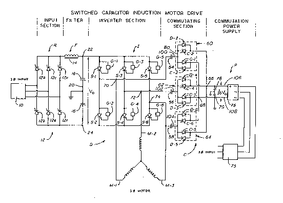
In the drawings, the letter D designates generally a
switched capacitor induction motor drive according to the
present invention. Referring now to Fig. 3, drive D
includes an input circuit R, a filter circuit F, an
inverter circuit I, a commutating circuit C, and a
commutation power supply P.
Input circuit R includes a three-phase alternating
current line input 10 and a conventional six element,
three-phase bridge rectifier 12. Rectifier 12 converts
line alternating current voltage to direct current voltage
which is impressed on filter F. ~otor voltage control is
achieved in conventional manner by controlling the phase
timing of silicon controlled thyristors 12a, 12b, 12c,
12d, 12e, and 12f which form rectiEier bridge 12. The
details of the conventional motor voltage control do not
~orm a part of the present invention and thus are not
illustrated in Fig. 3.
Filter F includes inductor 1~ and non-polarized
capacitors 16, 18. Capacitors 16, 18 form a series
~348~ 8
--7--
circuit path at the ou~put of the filter F ancd are each
connected to a common neutral terminal 20. Input circuit R
and filter F thus provide a D.C . link voltage VD at
terminals 22, 2~ which is impressed upon inverter circuit I.
Inverter circuit I includes six switching elements Sl-S6
which form a force commutated inverter bridge to provide an
output drive voltage to three-phase motor M. Switches Sl-S6
may be any suitable switching element capable of reverse
voltage blocking, such as insulated gate transistors or
conventional thyristors, for example. In the preferred
embodiment, swltches Sl-S6 are silicon controlled rectifiers
or thyristors. The unique commutation and switching control
circuitry of the present inventon permits the use of
relatively inexpensive, readily available thyristors ~or
switches Sl-S6 which are only exposed to relatively low rates
of voltage change during switching. For example, switches
S1-S6 experience about one-half volt per microsecond during
switching for a two-hundred-thirty volt alternating current
, motor drive.
Inverter I also includes thyristor switching control
circuits G-l through G-6 associated with thyristors S-l
through S-6, respectively. The details of circuits G-l, G-6
are illustrated in Fig. 6.
The switching of each thyristor S is dually controlled
by commutation circuit C and by control circuit G. Control
circuit G ensures that thyristors S are not enabled unless
the voltage difference from anode to cathode on the respective
thyristor S is within prescribed low limits. In this manner,
inexpensive, readily available thyristors can be used for
switching, and the need for free-wheeling anti-parallel diodes
around switches Sl-S6 is eliminated~ One advantage obtained
by eliminating these diodes, is that switches Sl-S6 may be
reverse biased during commutation. Another advantage is that
;n the drive of the present invention the need eor snubbering
is eliminatecl and the losses and adverse operating effects
caused by harmonics introduced in conventional high voltage
switching drives are greatly reduced.
Referring now to Fig. 6, control circuit G-l, which
is identical in all respects to circuits G-2, G-6, is
~28~
--8--
connected to the gate 37 and anode 28 of thyristor S-l in
the manner illus-trated. Control circuit G-1 includes PNP
gate drive transistor 30 and a series resistor voltage
divider network 32 connected to the collector of
transistor 30 to provide enabling gate current to SCR S-1
when appropriate. The emitter of transistor 30 is
connected ~o a low level positive direct current voltage
supply 34, which may be fixed, for example, at positive
six volts D.C. The collector of transistor 30 is
connected through divider circuit 32 to a low level
negative direct current supply 36 which may be fixed, for
example, at negative five volts. A capacitor 38 is
provided between the gate 37 and cathode 39 of SCR S-1 to
delay briefly the enabling of SCR S-1 after a positive,
enabling voltage is applied to gate 37 and to assist
disabling SCR S-1 when the voltage applied to cathode 39
is reversed in the manner described hereafter.
The primary purpose of circuit G-l is to enable SCR
S-1 for motor control, and to do so only when the vol-tage
across rectifier S-1 is within prescribed low limits.
Rectifier S-1 is enabled/disabled by providing/removing
gate drive via transistor 30. Transistor 30 is enabled,
and the voltage to gate 37 is made positive with respect
to cathode 39 only when two condi-tions are satisfied: (a)
the voltage across rectifier S-1 is within prescribed
limits; (b) opto-isolator 40 is enabled in response to a
fre~uency dependent enabling signal generated by
conventional motor frequency control circuit 42 which is
illustrated schematically in Fig. 6. Circuit 42 provides
a Erequency dependent enabling signal to opto-isolator 40
to control the frequency of switching to to affect motor
control in the convention~l manner.
Control circuit G-1 also includes rectifier 44 and
resistor 46 in the collector circuit of opto-isolator 40.
As can be seen by referrincJ to Fig. 6, transistor 30 is
only enabled when opto-isolator 40 :is enabled in response
to a control signal from motor frequency control circui-t
~2~ 8
_9_
42 and when the voltage applied to diode 44 is sufficient
to ~orward bias diode ~4 and allow base current to be
provided to transis-tor 30. Thus -transistor 30 is enabled
only when -the voltage at terminal 2~, i.e., -the voltage
applied to SCR S-l, is su~iciently low so that diode 44
is ~orward biased by the voltage provided via low voltage
DC supply 34 across diodes 4~ and resistor ~6. In this
manner, recti~ier S~l is enabled only when the voltage
across rectifier S-l, i.e., from terminal 28 to terminal
39 is less than a prescribed minimum so as to achieve low
dV-dT switching of control rectifiers S-l through S-6.
Diodes 48 (Fig. 6) are provided -to protect opto-isola-tor
40 from excessive voltages when rectifier S-l is reversed
biased. The value of resistor 46 is selected so as to
prescribe the maximum switching volkage which will be
permitted, which in the preferred embodiment is
approximately five volts. Resistor 50 and capacitor 52
are provided in the emitter to base circuit of transistor
to delay turn-on o~ transistor 30 after both
opto-isolator 40 and diode 44 are enabled.
Two alternate gating circuit designs are shown in
Figs. 7 and 8. The gating circuit of Fig. 6 provides gate
drive when the circuit has been enabled and when the
anode-cathode voltage across the thyristor or switch S-l
drops below a low reference voltage. The two alternate
circuits provide gate drive only when the gate drive
circuit has been enabled and the anode-ca-thode voltage
level is increasing, regardless of its value. This
eliminates the possible switching of the thy.ristor S-l by
-the initial low voltage drop across it, thereby
eliminating a small currenk surge. The circu:its allow the
thyristor S-l to be switched if the anode-cathode voltage
does not decrease below a small reference value, enabling
the motor drive D to deliver power during certain line
dis-turbances. Additionally, ga-te drive power is conserved
` because no drive is provided after the thyristor S-l
10-
begins conduc-ting as the anode-cathode ~oltage remains
constant in this state.
The circuits shown in Fig. 7 and 8 work similarl~,
but are enabled dif~erently. Fig. 7 is enabled by using
an opto-isolator 142 while the circuit of Fig. 8 is
enabled by a switchable voltage source whose output is
represented by the wave form 156. This signal 156 can be
developed from a controlled high fre~uency -transformer and
xectifier circuit or other commonly available circuits.
Io Referring now to Fig. 7, a resistor 132 is used to
dissipate gate current in the thyristor S-1 to provide
positive turn off. The circuit includes a PNP gate drive
transistor 136 and has a series limit resistor 13~
connected between the collector of the transistor 136 and
the gate 37 of thyristor S-l. Connected between the
collector of transistor 136 and the cathode 39 of
thyristor S-l is a Zener diode 130 used to protect the
gating circuit. The emitter of the gate drive transistor
136 is connected to a low level positive direct current
voltage supply 34, which may be fixed for example at
positive 5 volts D. C.
A vol-tage change sensing portion of the circuit is
connected between the anode 28 and the cathode 39 of
thyristor S-l. The voltage change sensing portion
consists of a series combination of a voltage sense
capacitor 152 and a curren-t limit resistor 150 which is
connected to the base of an NPN transis-tor 144 whose
emitter is connected to the cathode 39. A parallel
combin~tion of a diode lg8 and a resiskor lg6 are also
connected between the base of transis-tor 144 and the
cathode 39 to provide reverse circuit protection and
efective circuit kurno~f.
The collector of the voltage sense transistor lg4 is
connected to the base of the gate drive transistor 136
35 through a series combination of a resis-tor 154 and an
opto-isolator 142. When the rate of voltage change
between the anode 28 and the cathode 39 is sufficiently
~ %~ 8
positive to turn on the voltage sense transistor 144 and
the opto-isolator 142 is enabled, a base current path is
provided ~or the gate drive transistor 136, enabling the
thyristor S-1 to switch.
A parallel combination o~ a resistor 138 and a
capacitor 140 are connected from the emitter to the base
o~ gate drive transistor 136. The resistor provides
positive turno~f characteristics and the capacitor
provides a ~iltering ~unction to limi-t the transients in
the system from accidentally activating the thyristor S-l.
The circuit of Fig. 8 is similar to that of Fig. 7
with the exception that the opto-isolator lg2 is removed
and the low level positive voltage supply 34 is replaced
with a switchable voltage source as shown by the wave ~orm
156.
Commutation circuit C includes motor-run capacitors
54, 56 and 58 connected at one end to motor winding
circuits M-l M-2, and M-3, respectively (Fig. 3~ and on
the other end using conduc-tors 100, 102 and 104
respectively, to commutation thyristor and diode networks
60, 62 and 64, respectively. Thyristor/diode networks 60,
62 and 64 provide a circuit path from windings ~-1, M-2
and M-3 through capacitors 54, 56, and 58, respectively to
power supply P to permit capacitors 54, 56 and 58 to
absorb recirculation current ~rom motor terminals M-l, M-2
and M-3 during switching. Capacitors 54, 56 and 58
additionally provide reverse bias voltage .~or commutation
o~ thyristors S-1 through S-6 in the manner described in
detail below. Thyristor/diode networks 60, 62 and 64 are
connected in anti-parallel pairs with polarities aligned
in the manner illustrated in Fig. 3. Networks 60, 62 and
64 transmit voltage changes from terminals 66 and 68 to
terminals 70, 72 and 74 via capacitors 54, 56 and 58,
respectively to provide reverse bias voltage to force
commutate main thyristors S-l through S-6.
Two alternate thyristor/diode networks are shown in
Fig. 4 and Fig. 5. Under certain transient operating
~LZ'~
-12-
conditions, for example, when the voltage on the main
power capacitors 16 and 18 is increasing, a relatively low
current may be flowing through ~ first network thyris-tor
when a second opposing thyris-tor is ya-ted on. This may
result in a failure of the commutation power supply P
unless a means is provided to commutate -the relatively low
current flowing -through -the ~irst network thyris-tor. Two
al-ternative circuits for doing this are shown in Fig. 4
and 5.
The two designs utilize sa-turable
transformer/reactors 114 and 120 and 124 and 126 in series
with thyristors 112 and 118, respectively. The saturable
reactors reverse bias -the first network thyristor for a
time sufficient to commutate the thyristor when the second
network thyristor is gated on. The post-satura-tion
reactance of the saturable transformer provides reverse
current rate change limitation for the thyristor being
commutated. A typical design will provide 50
microseconds of reverse bias to the thyristor being
commutated and the saturation curren-t will be
approximately 10% of the maximum commutation current~ A
relatively small capacitor 122 can be placed be-tween the
conductor 100 and ground to limit voltage change ra-tes.
Commutation power supply P is fixed relative to the
neutral terminal 20 and provides low level, direct current
commutation voltage to commutation circuit C. Power
supply P includes conventional three-phase inpu-t
transformer 75 which steps the voltage down from input
line power 10 to provide approximately one percent of
drive input power to a conventional three-phase ~ull wave
rectifier 76. Rectifier 76 provides a direct c~lrrent
voltage output on buses 106 and 108 at capaci-tors 78 and
79 to drive the commutation circuit C in the manner
described hereinafter. ~he values of capacitors 78 and 79
and the other components of circuit P are selected to
provide an outpu-t voltage on capacitors 78 and 79 which is
typically ive to ten percent of the drive voltage Vd.
-13-
Self-commutating switching elements such as insulated gate
-transistors or transistor controlled thyristors do not
require this external commutation circuitry. ~Iowever,
they do reguire the motor-run capacitors.
The motor drive D allows braking of a load once the
load has ~een brought up to a given speed and is desired
to be reduced to a slower speed or stopped. If braking is
done, power will be generated by the transfer from kinetic
energy of the load to electrical energy in the drive D and
during this regeneration interval a por-tion of this energy
is fed into the commutation power supply P. This power
must either be dissipated or returned to the input line to
prevent damage to the circuitry. The maximum amount of
power that needs to be dissipated is about 3% of the full
power rating of the drive.
The simplest techni~ue to dissipate the excess
commutation power is shown in Fig. g and is a simple
resistive dissipation technique. A power resistor 160 is
connected in series with a switch 162 and connected
between the output buses 106 and 108 of the commutation
power supply P. When the switch 162 is in the closed
position the power resistor 160 will provide power
dissipation and therefore allow regeneration to occur.
The switch 162 is preferably controlled by a control
circuit having hysteresis 16g so that the switch 162 is
operated in a digital mode with sufficiently long closed
position intervals. Additionally, the power resistor 160
is pre~erably connected only during regeneration, thereby
not decreasing the overall e~ficiency of the drive D. The
s~itch 162 may be a transistor, a gate turn-off thyristor
or a force-commutated thyristor circuit.
A higher eficiency design is shown in Figs. 10 and
ll where the three-phase full wave rectifier 76 in the
commutation power supply P is replaced by a
self-controlled, transis-tor inverter 250. This inverter
250 allows the regeneration power -to be retransmitted to
the input three phase system therefore eliminating the
~2~
-14-
need ~or the power resistor and heat dissipation
requirements of the resistive circuit. The circuit
there~ore increases the overall system e~iciency on a
longer term basis as well as a shorter term basis.
The circuit 250 has the same general ~orm as a full
wave three-phase rectifier circuit wi-th the addition o~
~TPN transistors and drive circuits in anti-parallel with
the rectiication diodes. In Fig. 10 the pairs are diode
170 and transistor 172, diode 174 and transistor 176,
diode 178 and transistor 180, diode 182 and transistor
184, diode 186 and transistor 188 and diode 190 and
transistor 192 ~orming the six pairs. It showld be noted
that the inverter transistors are shown as single NPN
transistors in Fig. 10 and in Fig. 11 the transis-tors are
shown as a Darlington pair. When the motor drive D is
delivering motoring power and is not regenerating, all the
transistors are turned off and the circuit behaves as a
standard three-phase rectification bridge with inductor
194 and capacitors 78 and 79 providing the filtering
necessary for the commutation power supply P.
When the circuit is in the braking or regeneration
mode, the transistors are activated. An exemplary
diode-transistor pair 206 is shown in Fig. 11 with the
gate drive circuitry required to activate the inverter
transistors. The gating circuit is designed to allow the
inverter transistors to conduct whenever the
collector-emitter voltage across the transistor is less
than about three volts.
A low level, positive direct current voltage supply
224, similar to -the voltage supply 34, is connected to the
emitter o~ the commutation gate drive PNP transistor 218.
The collector of the transistor 218 is connected through
current limiting resistor 216 which is connected to the
base drive circuit of the ~arlington transistor of pair
206. A positive turn-off resistor 220 is connected
between the emitter and base of -the commutation gate drive
transistor 218 and a series combination of a current limit
- 1 5--
resistor 222 and a diode 226 is connected between the base
of transistor 218 and the positive inverter rail 202. The
diode 226 pro~ides reverse circuit protection by blocking
any current flow when the voltage of the rail 202 is
higher than the low level voltage source 224. This
blocking a~fect in combillation with the various voltage
drops of the circui-t and the level selected for the low
level voltage 22g allow transiskor 218 to be turned on
only when the voltage difference between the rail 202 and
lo the three-phase input line 204 is less than about three
volts. Preferably, the low level voltage 224 is enabled
only when the drive is in regenerating mode and not when
the drive is in motoring mode, thereby further improving
overall drive efficiency.
The commutation inverter circuit operates generally
as follows. Inverter transistors 172 and 192 are
conducting with the remaining transistors being turned off
because the voltage across them exceeds the preferable
three volts. The voltage of the input line 244 is
approaching the voltage of input line 242 and is
increasing. As the voltage of line 244 increases and
exceeds the voltage of line 242, curren-t begins to flow
through diode 17~ adding current to the main current
flowing through inverter transistor 172. This current
quickly builds in diode 174 and inverter transistor 172,
causing the voltage across inverter transistor 172 ko
increase because the inverter transistor 172 saturates.
This voltage increase removes -the base drive from inverter
transiskor 172, turning off inver-ter transistor 172. When
inverter transistor 172 turns off, an excess current is
then flowing through the leakage inductance of the
three-phase line 242 and 24~, which is dissipated in
~oltage suppressor 196 because the current flowing through
transistor 172 is diverted in-to voltage suppressor 196 and
diode 182. This excess current is quickl~ dissipated and
the main current switches to kransistor 176. This process
continues for the remaining phases.
-16-
This drive supplies three-phase adjustable frequency
and vol-tage drive to a three-phase induction motor.
Voltage is supplied to the output sec-tion by the
previously described input and filter sections.
Alternating current is supplied to the motor by al-ternate
conduction of each thyristor in a bridge. Balanced
-three-phase output is achieved in the conventional manner
by consecutively switching the polarity of the bridges.
Since silicon controlled rectifiers, or SCR's must be
externally commutated, the commutation section C and
commutation power supply P are provided to allow for
external orced commutation of the main SCR's.
Start up cf the drive is accomplished by applying a
low voltage to the inverter section I with one SCR on each
of the three output bridges enabled. One bridge has a
polarity opposite o~ the other two. Current begins to
10w through the motor windings from the applied voltage.
Additionally, commutating SCR's C-l through C-6 are
enabled when corresponding main SCR's S-1 through S-6 are
on and are disabled when their corresponding SCR's S-l
through S-6 are of~, the correspondence being shown in
Fig. 3. This correspondence is established by opposite
polarity. For example, commutation SCR C-1 on the low
voltage side of the commuta-tion power supply P corresponds
to, and is enabled simultaneously wi-th, main SCR S-1 on
the high voltage side of the inverter section.
Clocking o -the inverter I begins when a main SCR S
is commutated. The commutation process will be
illustrated by example. A commutation is initiated by
first removing gate drive from a main SCR such as S-1, for
example, which is to be commutated and its corresponding
commutation SCR, C-1. After a short time, typically 100
microseconds, the gate circuits of the main SCR in the
opposite position of the output bridge, i.e., S-2, and its
corresponding commutation SCR C-2, are enabled. SCR S-2
will not receive gate current because Diode gg in Fig. g
is reversed biased as long as S-2 blocks more than
-17-
typically 5 volts in the forward direction. Prior to the
co~nutation of SCR S-1, terminal 80 on motor run capacitor
54 is at the lower potential of commutation Power Supply
P. When SCR C~2 is enabled, it -turns on, thereby quickly
raising terminal 80 to the higher potential of P. This
causes the voltage at terminal 70 connected to capacitor
54 to apply a reverse :bias voltage to S-l. Current
through SCR S-1 is stopped and quickly diverted into
capacitor 54, C-2, and P.
SCR S-1 is reverse biased by typically 30 volts for a
230 volt dr.ive. Its gate also receives a nega-tive bias to
speed turn-off. Current flow through SCR C-2, capacitor
54 and motor winding M-1 causes a voltage rate of change
of typically 0.5 volts per microsecond across capacitor
54. Therefore SCR S-l will be reversed biased for
typically 60 microseconds. During this time, SCR S-1
changes from the conducting to the non-conducting state.
~hen SCR S-l again sees forward bias voltage, the
rate-of-voltage-change is still typically 0.5 volts per
microsecond for a 230 volt drive. This low dV/dT reduces
the required reverse bias voltage by reducing the
effective turn-off time.
A significant amount of time, typically 600
microseconds, is required for the voltage across SCR S-2
to become low enough for gate drive to be applied to it.
During this -time, neither SCR S-l nor SC~ S-2 are
conducting. The motor leakage inductance exchanging
energy with motor run capacitor 54 is responsible for this
low dV/dT and relatively long quiescent time. Typically
this leakage inductance is sufficient to cause the voltage
across SCR S-2 to become negative, as capacitor 54
continues to absorb the motor recirculation current. At
some point, current flow through winding M-1, capacitor
54, and SC~ C-2 stops and reverses since winding M-1 now
has a negative, with respect to motor neutral, voltage on
it. ~ntil SCR S-2 is forward biased again, cuxrent flows
through capaci-tor 54 and anti-parallel diode D-2. When
-18-
SCR S-2 becomes forward biased, current is transferred
from capacitor 44 and diode D-2 into SCR S-2 and flows
into terminal 24. Current flow through SCR C-2 has ceased
and is therefore "off".
Current flow through SCR S-2 continues until its
half-cycle is complete, and SCR C-l is enabled to begin
the commutation of SCR S-2. The commutation process on
the other two output bridges is identical.
Drive control consists of driving the inverter
section I, via motor control circuit 42, at the frequency
selected b~ manual or automatic external control. The
output voltage is determined by the frequency and the load
on the motor. Generally, higher frequency calls for a
higher voltage and more load calls for a higher voltage
and vice-versa. Voltage must be controlled accurately
with load, because there are no recirculation diodes in
the inverter section to accommodate low power factor.
Therefore, the voltage control used in association with
the drive of the present invention should raise or lower
the voltage as required by the load and frequency control
to maintain the optimum power factor on the output. Power
factor sensing can be done by any of several well known
techniques.
The foregoing disclosure and description of the
invention are illustrative and explanatory thereof, and
various changes in the size, shape, materials, components,
circuit elements, wiring connections and contacts, as well
as in the details of the illustrated circuitry and
construction may be made without departing ~rom the spiri-t
of the invention.