Note: Descriptions are shown in the official language in which they were submitted.
. ~8~ 27371-157
Thls application is related to the subject matter of
Canadian Patent No. 1,2~7,223 issued Decem'oer 20, 198~.
BACKGROU~D O~ TME INVENTION
The present invention relates to a three-stage coupling
arrangement for an electrical data exchange system including
first, second and third stages, each stage comprising a plurality
of coupling matrixes each of which has inputs and outputs and a
matrix of switching points for selectively switching t'nrough
signals from the inputs to respective outputs; and intermediate
conductors for connecting the outputs of the coupling ma-trixes of
one stage with the inputs of the coupling matrixes of a next
stage: wherein the inputs of the coupling matrixes of the first
stage constitute the inputs of the coupling arrangement and the
outputs oE the coupling matrixes of the third stage constitute the
; outputs of the coupling arrangement.
Coupling arrangements are used to selectively connect
signal sources with signal drains. There are single-stage
coupling arrangements and multi-stage coupling arrangements. A
three-stage coupling arrangement is disclosed in an article ~y
Charles Clos, entitled, "A Study of Non-Blocking Switching
~- ~
)5 3
Networks", in the The Bell System Technical Journal, Volume
XXXII 1953, pages 406-424.
~ The coupling arrangement shown in Figure 2 of that
j article has a first stage, stage (a), a second stage, stage
(b), and a third stage, stage (c~. Each stage is composed of
a plurality of coupling matrixes. The coupling matrixes of
one stage differ in the number of their inputs and outputs
from those of the other stages. For example, the coupling
matrix of the first stage has six inputs and eleven outputs,
the coupling matrix of the second stage has six inputs and
six outputs and the coupling matrix of the third stage has
eleven inputs and six outputs. Thus, three different
embodiments of coupling matrixes are required. The number of
embodiments is reduced to two if the switching points employ
switching means which permit signal transmission in both
directions~ as is the case, for example, for metal contacts.
In such a case, the embodiment provided for the first stage
can also be used for the third stage with the inputs and
outputs exchanged.
This coupling arrangement is non-blocking. That is, for
every possible combination of already-existing aonnections
between a signal source and a signal drain every additional
connection which is appropriate merely on the basis of the
still available inputs and outputs can indeed be switched
5~
through. This is possible without a requirement for so-
called "recoupling" also called 'Irearrangement''.
SUMMARY OF THE INVENTION
It is an object of the present invention to provide a
coupling arrangement of the above-mentioned type in wXich the
coupling matrixes of all stages have the same configuration.
The above and other objects are accomplished in the
context of a three stage coupling arrangement for an
electrical data exchange system of the type first described
above, wherein the arrangement additionally includes: first
and second iden~ical three-stage switchboards between which
the coupling matrixes are distributed, each stage of each
switchboard having the same number of coupling matrixes, each
coupling matrix having a number of inputs equal ~o its number
:15 of outputs, each one of the inputs of the coupling matrixes
of the first stage of each respective switchboard consti-
tuting one of the inputs of that switchboard, each one
of the outputs of the coupling matri~es of the third stage of
-each respective switchboard constituting one of the outputs
of that switchboard, the inputs of the first switchboard
being positioned in an identical numbered sequence as the
inputs of the second switchboard, the outputs of the first
switchboard being positioned in an identical numbered
sequence as the outputs of the second switchboard, each input
1~8~
of the first switchboard heing connected with the identically
numbered input of the second switchboard, and each output of
the first switchboard being connected with an identically
numbered output of the second switchboard; and further
including:
a common control means connected with each of the first
and second switchboards for producing addresses identifying
switching points to be switched through, each address
including a designation of: the row and column of a switching
point within a coupling matrix; ~he number of a coup:Ling
matrix withln a stage; and the number of a stage within a
switchboard; the control means further having two outputs
and producing at such outputs respective switchboard
addresses identifying a respective one of the first and
second switchboards;
lines connected in parallel between the control means
and the inputs of the first and second switchboards for
carrying swi~ching point addresses to both switchboards; and
two individual lines each leading from a respective one
of the two switchboard outputs of the control means to a
respective one of the switchboards for carrying a
corresponding switchboard address to that switchboard.
The connection of each input and output of a first
coupling field (switchboard) with an input or output,
respectively, of a second coupling field (switchboard) is
~28~()5.~
known per se from the German periodical l'Vnterrichtsblatter
der Deutschen Bundespost" [Instructional Sheets From the
German Federal Postal Service], Volume 33/1980, No. 12, page
475, Figure 13. However, the parallel connection of coupling
fields realized in this manner is limited to two stages of a
four-stage coupling arrangement.
BRIEF DESCRIPTION OF THE DRAWINGS
The present invention will be described with reference
to the accompanying drawings, wherein:
Figure 1 is a block circuit diagram of a coupling
arrangement according to the invention.
Figure 2 is a block circuit diagram of one of the
identical coupling fields KF1 or KF2.
Figure 3 is a schematic showing ~he mechanical structure
of two switchboards each containing a respective one of the
coupling fields KF1 and KF2.
Figure 4 is a block circuit diagram showing a common
control for the ~wo coupling fields KF1 and KF2.
Figure 5 is a schema~ic illustration of the mechanical
arrangement of three magazines M1 to M3 on top of one
another.
Figure 6 is a schematic of a connector module circuit
board provided with a matrix of switching points.
-- 6 --
~%8~0~
Figures 7 to 9 together comprise a schematic of a rear
wall circuit that can be utilized to connect the connector
module circuit boards of adjacent magazines of a coupling
field.
Figure 10 is a schematic sectional view of a rear wall
circuit board showing the offset positioning of conductors or
conductor pairs accor~ing to another aspect of the invention.
Figure 11 is a schematic showing two switchboards KFl
and KF2 and respective rear wall circuit boards L3 disposed
therein.
Figure 12 is a block circuit diagram of a control
; circuit for two switchboards KFl and KF2.
Figure 13 is a schematic of an embodiment of a switching
matrix employed according to another aspect of the invention.
Figure 14 is a schematic showing the structural
relationship of two switchboards KFl and KF2 each including
magazines Ml and M3 along with a fourth magazine M4 comprised
of switching matrices of the type shown in Figure 13.
Figure lS is a schematic showing two flat cables
arranged for connecting the outputs of two switchboards to
the inputs of coupling matrixes.
DESCRIPTION OF THE PREFE~RED EMBODIMENT
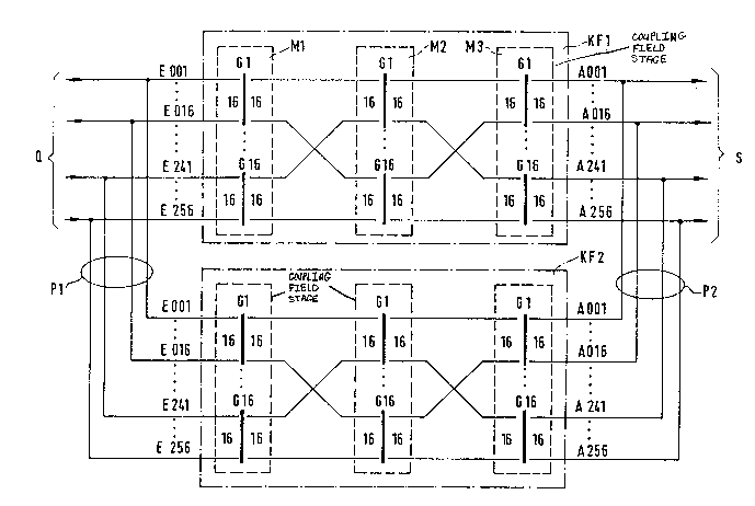
Referring to Figure 1, there is shown a coupling
arrangement composed of a first coupling field KFl and a
~2~ )S~
second, identical coupling field KF2. Each coupling field is
composed of a first stage Ml, a second stage M2 and a third
stage M3, i.e. each coupling field is composed of three
stages. Each stage has 16 identical coupling matrixes
Gl to G16, with each coupling matrix having 16 inputs and 16
outputs.
Each input of a coupling matrix of the first stage is an
input o~ the respective coupling field. For 16 coupling
matrixes Gl to G16 each having 16 inputs, there results 256
inputs E001 to E256 for each coupling field KFl and KF2,
respectively. In the same manner, the outputs of the
coupling matrixes of the third stage of each coupling field
form 256 outputs A001 to A256.
By way of a first parallel wire connection Pl, each one
of the inputs E001 to E256 of the first coupling field KFl
is connected with the identically numbered input of the
second coupliny field KF2~ Outputs A001 to A256 are
connected in the same manner, by way of a second parallel
wire connection P2. In this way, the two coupling fields KFl
and KF2 are connected in parallel. Additionally, 256 signal
sources Q are connected with inputs E001 to E256 and 256
signal drains S are connected with outputs A001 to A256.
Figure 2 shows a block circuit diagram for the first and
second coupling fields KFl and KF2, respectively. Again
shown are the first stage Ml, the second stage M2 and the
- 8 --
12~35055
i third stage M3 and the coupling matrixes G1 to G16 of which
each stage is formed. Each coupling matrix is composed of
256 switching points KP which are arranged in a 16 x 16
matrix. The inputs E1 to E16 and the outputs A1 to A16 of
each coupling matrix are also shown.
The inputs E1 to E16 of each of the 16 coupling matrixes
G1 to G16 of the first stage M1 form the 256 inputs E001 to
E256 of coupling fields KF1 and KF2, respectively. Similar-
ly, the outputs A1 to A16 of each of the 16 coupling matrixes
G1 to G16 of the third stage M3 form the 256 outputs A001 to
A256 of coupling fields KF1 and KF2, respectively.
The outputs A1 to A16 of each coupling matrix G1 to G16
of the first stage M1 and of the second stage M2 are connect-
ed, via systematically guided intermediate lines, with
the inputs E1 to E16 of coupling matrixes G1 to G16 of the
second stage M2 and the third stage M3, respectively. The
system for these intermediate lines is as follows:
The ordinal of an output or input, respective-
ly, is e~ual to the ordinal of the coupling matrix
with which this input or output is connected.
In the embodiment described here, this means that the
connections are as shown in Figure 2, namely:
a) all first outputs, i.e. A1, of the coupling
matrixes G1 to G16 in the first stage M1 are connected with
the first coupling matrix Gl of tne second stage M2; all
'
s~
second outputs A2 of the coupling matrixes G1 to G16 in thefirst stage M1 are connected with the second coupling matrix
G2 of the second stage M2, etc.;
b) all first inputs E1 of the coupling matrixes G1
to G16 of the second stage M2 are connected with the first
coupling matrix G1 of the first stage M1; all second inputs
E2 of the coupling matrixes G1 to G16 of the second stage M2
are connected with the second coupling matrix G2 of the first
stage M1, etc..
The connections sta~ed under a) and b) above apply
in a similar manner to the intermediate connections between
the second and third stages, M2 and M3, respectively.
Figure 3 shows the mechanical structure of two
; switchboards, one for each coupling field. To make this
; 15 association clearer, the switchboards are identified with the
respective identifications of the coupling fields, i.e. KF1
and KF2, respectively. Each switchboard has a first magazine
M1, a second magazine M2 and a third magazine M3. Each
magazine includes the 16 coupling matrixes G1 to G16 of a
stage. The identical reference numerals M1, M2 and M3 for
the magazines and for the stages in Figures 1 and 2 indicate
their respective associations.
Each coupling matrix is configured as a connector
module. Since, according to Figure 1 or 2, each stage has 16
coupling matrixes, each magazine also contains 16 connector
-- 10 --
\
~2~35055
modules. These 16 connector modules are shown in the first
- magazine Ml of the first switchboard KFl. The first module
is identified as Gl and the last module as G16O By selecting
the same reference numerals Gl to G16, the association with
the coupling matrixes shown in Figures 1 and 2 is again
clear. Pl and P2 identify first and second parallel wire
- connections between coupling fields KFl and KF2
The control of the two coupling fields KFl and KF2 by
means of a common control St will be described with reference
to Figure 4. This control includes four output lines for
carrying the address corresponding to respective switching
points to be switched through, i.e. for the column address
Sp.-A., the row address Z.-~. and for the coupling matrix
address Km.-A. Two outpu~ lines are provided for carrying
the stage address St.-A. These outputs ar~ each connected by
means of four or two wires~ respectively, with the identical-
ly named inputs of coupling fields KFl and KF2. Since,
corresponding to its 16 inputs and 16 outputs, each coupling
matrix has 16 columns and 16 rows, each stage has 16 coupling
matrixes and each coupling field has three stages, it is
sufficient to have four wires for each one of the column, row
and coupling matrix addresses and two wires for the stage
address in order to unequivocally identify each switching
point to be switched through if binary coding is employed.
The respective switchboard or coupling field KFl or KF2 is
-- 11 --
~%$~5~
identified by individually guided wires which connect the
two outputs Schr.-A.l and Schr.-~.2 for ~he switchboard
addresses with the respective inputs Schr~-A. in switchboards
KFl and KF2.
Each one of coupling fields KFl and KF2 individually
already permits the connection of each input with any desired
output. However, blocking may occur; that is if a plurality
of connections have already been establishedr a further
connection from a certain input to a certain output can no
longer be switched through. The parallel connection of two
such coupling fields according to the invention avoids such
blocking so that the coupling arrangement according to the
invention is non-blocking.
According to a further aspect of the invention, error-
free production of the intermediate lines is permittedwithout significant manual labor. This modification will be
described with reference to Figures 5 to 9.
Referring first to Figure 5, there is again shown the
three magazines Ml to M3 in their mechanical arrangement one
above the other. The first magazine Ml is at the top, below
it the second magazine M2 and at the bottom the third
magazine M3. They are mechanically connected with one
another in a manner not shown. The second magazine M2 is
thus adjacent to the first magazine Ml as well as to the
third magazine M3.
- 12 -
0~5
Each magazine has 16 guide strips F at its top and 16
guide strips F at its bottom into which are brought the 16
connector modules on which the coupling matrixes G1 to G16
are supported, respectively. Only the bottom guide strips F
are shown~ Of the 48 connector modules ~16 per magazine),
only the sixteenth connector module G16 of the third magazine
M3 is shown. Each connector module is equipped with a multi-
point connector having a first pin strip S1 and a second pin
strip S2. Instead of the two pin strips S1 and S2, a single,
large pin strip may also be provided.
Moreover, a first rear wall circuit board L1 and a
second rear wall circuit board L2 are shown. Each such rear
wall circuit board is equipped with two rows of 16 socket
strips as receptacles, with socket strips B1 to B16
constituting the upper row and socket strips B17 to B32
constituting the bottom row. Socket strip B17 and a few
other, unidentified socket strips are not visible here. Also
provided are a third rear wall circuit board L3 and a fourth
rear wall circuit board L4. These are each e~uipped with
only one row o 16 socket strips B33 to B48 and B49 to B64,
respectively.
Dashed lines indicate into which one of the guide strips
the illustrated connector module G16 is brought when it is
plugged in, which position the rear wall circuit boards take
up at the rear of the magazines after assembly, and that
13 -
~2~5~5~
connector strips Sl and S2 of the illustrated connec~or
module G16 engage in socket strip B32 of the second rear wall
circuit board L2 ~nd in socket strip B64 of the fourth rear
wall circuit board L4. In the same manner, the connector
strips of the connector modules that are not shown engage in
their associated socket strips. Thus, an association
results as shown in the table below:
Connector Modules Connector Rear Wall Socket
Gl to G16 in strip circuit board strips
_ magazine Sl L3 _ B33 to 48
. _ . _ Sl Ll B17 to B32
M2 S2 _ _ ~ ~~ B 1 to B16
M3 Sl L2 B49 to B64
If, instead of the two connector strips Sl and S2,
a single, large connector strip is provided, the respective
part of this strip engages in the corresponding part of the
socket strip according to the table above.
Thus, rear wall circuit board Ll includes the region of
connector strips S2 of the first magazine Ml and the xegion
of connector strips Sl of the second magazine M2. The region
of connector strips S2 of the first magazine ~1 is adjacent
the region of the connector strips Sl of the second magazine
M2. The same applies appropriately for rear wall circuit
board L2.
Figure 6 shows one of the connector modules Gl to G16.
It is composed of a circuit board LP which is provided with
- 14 -
~285~3~5
the 256 switching points KP arranged in a 16 x 16 matrix, a
first connector strip Sl and a second connector strip S2.
Circuit board LP is provided with conductor paths LB which
interconnect switching points KP and connect them with the
sixteen inputs El to E16 and the sixteen outputs Al to A16 on
connector strips Sl and S2, respectively. Inputs ~1 to E16
are all brought to the first connector strip Sl; outputs Al
to ~16 are all brought to the second connector strip S2. As
can be seen in Figure 5, in the connector modules of the
second magazine M2, the first connector strip Sl lies closest
to the first magazine Ml. Therefore, inputs El to E16 are
brought to this s~rip since they must be connected, according
to Figure 2, with the outputs of the connector modules of the
-~ first magazine Ml. The same applies correspondingly for the
; 15 second connector strips S2 and for the connector modules of
the other magazines.
Conductor paths LB are here shown as having but one
pole. However, since coupling fields are usually constructed
with two or even four conductors, one must imagine that two
or four conductor paths, respectively, are represented by
one line and the corresponding number of plug-in pins are
provided on the connector strips.
Figures 7, 8 and 9 show one of the rear wall circuit
boards Ll and L2. These figures should be placed next to one
another, Figure 7 on the left and Figure 9 on the right.
- 15 -
~35~55
The upper and lower lines, respectively, as well as the left
line in Figure 7 and the right line in Fiyure 9 represent the
outlines of this rear wall circuit board. The locations for
socket strips Bl to B32 are marked ~1 to B16 (upper row) and
B17 to B32 (lower row~. The socket strips themselves are not
shown; the dots merely indicate the soldering spots for their
soldered pins. If one looks at the first rear wall circuit
board Ll, Figures 5 and 6 indicate that outputs Al to A16 of
connector modules Gl to G16 of the first magazine Ml are
lo placed on socket strips Bl to B16. Inputs El to E16 of the
connector modules of the second magazine M2 are placed on
socket strips B17 to B32, beginning each time at the top with
El and Al, respectively.
The intermediate lines which must be providecl according
to Figure 2, are formed by conductor paths LB'.
single-pole illustration has again been selected here; and
again, instead of one line, one must imagine two conductor
paths since, as indicated by the illustration of two
soldering spots for each input and output, the rear wall
circuit board shown here is intended for a two-wire coupling
field. Of the many intermediate lines, only a few are shown
here. It is also not shown that the conductor paths are
distributed to different planes of a multilayer plate so as
to accommodate their large number and to be able to cross
them over.
- 16 -
~;~8~
The second rear wall circuit board is designed like the
first since, according to Figure 2, the system of guiding the
j intermediate lines between ~he first stage and the second
^I stage is the same as betw~en the second stage and the third
stage.
The 256 inputs E001 to E256 of the respective coupling
fields KFl and KE'2 are brought to socket strips B33 to B48 of
the third rear wall circuit board L3 and the outputs A001 to
A256 of the respective coupling fields KFl and KF2 are
brought to the socket strips B49 to B64 of the fourth rear
wall circuit board L4 (see Figure 5). The soldering pins of
these socket strips are connected to the parallel wires Pl
and P2 as well as to the leads to signal sources Q and signal
drains S.
Not shown are switching means and control lines for
switching through and switching off the ~witching points KP.
This also applies for the multi-point connector modules.
According to yet a fur~her aspect of the invention,
; suEficient crosstalk attenuation can be maintained between
conductox paths of the rear wall circuit boards for the
: transmission of digital signals at a bit rate up to 150
~Ibit/s. Such high crosstalk attenuation is achieve~ with the
use of a multilayer circuit board as shown in Figure 10.
Figure 10 is a sectional view of a rear wall circuit board,
such as Ll or L2, showing the position of the conductor paths
- 17 -
~%~35~55
within it. The circuit board has 19 layers between which lie
the conductor paths which are shown by hatching. It is
assumed that the coupling field is constructed of two wires,
i.e. each connection is established in the form of a pair of
conductor paths~ The first pair is marked LBl and lies in
the first plane between the first and second layers. To
realize a sufficien~ly high crosstalk attenuation, the second
pair ~B2 is disposed in the next plane, i.e. the second
plane, not directly next to the first pair LB 1, but of~set
to the side to meet the reguirement for crosstalk attenua-
tion. This lateral offset extends over eight planes. The
ninth and tenth planes accommodate conductor paths StL for
the control lines not shown in Figures 7 to 9. The existing
crosstalk attenuation requirements do not permit the
placemPnt of a pair LB3 without offset with respect to the
first pair LBl before the eleventh plane.
~ ccording to one implementation, the layers are made of
a material of the type GF~ according to MIL P-13949F. The
thickness of a layer is .15 mm. The thickness of a conductor
path is .017 mm. The width of a conductor path is .2 mm.
The width of the gap between the conductor paths of a pair is
.2 mm. The size of the offset between conductor paths of
adjacent planes is 1.2 mm, measured between the middles of
the concerning pairs. The crosstalk attenuation achieved by
the described provisions is not less than 43 dB between the
- 18 -
)55
pairs of adjacent planes and not less than 47 dB between
those pairs of planes without offset, as for example between
the pairs of the first and eleventh plane or of the second
and twelfth plane and so on. The above described embodiment
of a multilayer board is suitable to transmit NRZ-signals
with a bit rate up to 300 Mbit/s.
The conductor paths of the rear wall circuit boards can
have no abutting faces. To avoid such abutting faces, bends
in the conductor paths at an acute angle are avoided entire-
ly, as shown in Figures 7 to 9, and bends at a right angle
are resolved to two obtuse angle bends. Instead of changing
the bends to obtuse angles it is also possible to provide a
rounded version. This also applies for the conductor paths
of the multi-point connector modules. If acute angle bends
cannot be avoided, they are also resolved to a plurality of
obtuse angle bends or are rounded off.
Signal sources Q are connected with inputs EOOl to E256
without reflection. This is accomplished as shown in Figure
11 which illustrates the two switchboards or coupling fields
KFl and KF2 and the rear wall circuit boards L3 disposed
therein. The dots represent soldering pins for socket strips
B33 to B48. An unidentified cable leads from signal sources
Q to socket strips B33 to B48 in the first switchboard KFl
and the wires of this cable are soldered to the soldering
~5 pins of these socket strips. Only a few of these wires are
-- 19 --
~l~8~55
shown. These soldering pins are further soldered to the
wires of the parallel cable P1. The other ends of the wires
of cable P1 are connected to the soldering pins of socket
strips B33 to B48 of the second switchboard KF2. These
soldering pins are also connected to resistors R. Their
resistance value is e~ual to the characteristic impedance of
the parallel wires P1 and of the cable coming from signal
sources Q. These resistors produce the necessary reflection-
free termination since the coupling matrixes themselves, due
- lO to their high input resistances, are unable to provide such a
termination. Instead of soldering, any other connection
techni~ue can also be employed. Resistors R and the cable
cominy from the signal sources may also be exchanged,
i.e. the cable terminates in second switchboard KF2 and
resistors R are disposed in first switchboard KF1.
The corresponding configuration of the "parallel cable"
at the output will be described with reference to Figure 12,
which shows the two switchboards KF1 and KF2, each with
their 256 outputs A001 to A256, as well as 256 electronic
20 switches U001 to U256. Each one o~ the outputs A001 to A256
is connected with the associated first or second input,
respectively, of the associated electronic switch U001
to U256. The outputs vf the electronic switches are connect-
ed with signal drains S. Moreover, the electronic switches
are provided with control inputs which are connected with a
- 20 -
~2~
switch control U.-St. Switch control U.-St. is able to
control the electronic switches U001-U256 into their first or
second switch position. The first switch position is shown
here in which the respective output of the firs~ coupling
field KFl is switched through to the respective signal drain
S.
Since the coupling matrixes Gl to G16 have terminating
resistances at their outputs, a simple parallel connection as
at their inputs is not possible. Rather, only one of ~he
respective outputs o~ coupling fields KFl and KF2, respect-
ively, must be switched through to the respective signal
drain S. This is accomplished by electronic switches U001 to
U256 in dependence on whether the respective connection was
switched through via the first coupling field KFl or the
second couplin~ field KF2. The setting information required
for this procedure is obtained by the switch control U.-
St. from column address Sp.-A., row address Z.-A., coupling
matrix address Km.-A., stage address St.-A. and switchboard
addresses Schr.-A.l and Schr.-A.2. For that reason, the
switch control U.-St. is connected with the outputs of
common control St which have already been mentioned in
connection with the description of Figure 4.
An advantageous embodiment of the electronic switches
will be described with reference to Figure 13. To avoid a
multitude of connector module types, the same coupling
- 21 -
matrixes are employed as electronic switches as they were
used in coupling fields KFl and KF2 and described in connec-
tion with Figure 6. Such a coupling matrix is also shown in
Figure 13 and there identified as GUl. Circles indicate the
256 switching points. Inputs El to E8 are connected with
outputs ~001 to A008 of the first coupling field KFl. Inputs
E9 to E16 are connected with outputs A001 ~o A008 of the
second coupling field KF2. Outputs Al to A8 of this coupling
matrix are connected with the associated eight signal drains
10 S.
The arranqement operates as follows: If, for example, a
connection is to be switched through to ~he signal drain
connected at output ~1 of coupling matrix GUl, either
the switching point connecting input El or input E9 with
output Al in this coupling matrix is switched through,
depending on whether the connection is established via the
first coupling field KFl or the second coupling field KF2.
In a similar manner, connections are established with the
other outputs. The switching points required in each case
are emphasized in Figure 13 by double circles.
The further outputs A009 to A256 of coupling fields KFl
and KF2 are connected together in the same manner. Thus,
there result 32 such coupling matrixes, their accommodation
being shown in Figure 14, wherein the two switchboards KFl
and KF2 contain, in addition to magazines Ml to M3, fourth
- 22 -
~Z~ 55
magazines M4 for accommodatlng the 32 coupling m~trixes GU1
to GU32. Coupling matrixes GU1 to GU16 are disposed in the
first switchboard KF1, and coupling matrixes GU17 to GU32 are
disposed in the second switchboard KF20
Figure 15 shows an advantageous wiring between outputs
A001 to A256 of coupling fields KFl and KF2~ respectively,
and the inputs E1 to E8 of coupling matrixes GU1 to GU32.
The soldering pins of socket strips B49 of the first coupling
field KFl and of the second coupling field KF2 are shown by
32 dots, respectively, to which are connected outputs A001 to
A016. Another 32 dots identify the soldering pins of the
socket strips to which inputs E1 to E16 of coupling matrixes
GU1 and GU2 are connected. Two flat cables BKl and BK2 are
provided, each having 16 juxtaposed pairs of conductors.
Outputs A001 to A016 of the first coupling field KF1 are
connected with the inputs E1 to E8 of coupling matrixes GUl
and GU2 by way of the first flat cable. Outputs A001 to A016
; of the second coupling field KF2 are connected with inputs E9
to E16 of coupling matrixes GU1 and GU2 by way of the second
flat cable. The flat cables are slit in the middle for a
- length sufficient to permit connection to the socket strips
of coupling matrixes GU1 and GU2.
In the same manner, the further outputs of coupling
fields KF1 and KF2 are connected with the associated coupling
- 23 -
~2~ 5~
matrixes GU3 to GU32 by means of further pairs of flat
cables.
The use of flat cables is made possible by the associa-
tion, described in connection with Figure 13, of eight
outputs of coupling fields KF1 and gF2 with each one of
inputs A1 to A8 and A9 to A16, respectively, of one of
coupling matrixes GU1 to GU32. The use of 1at cables makes
it possible for these connections to have electrical
characteristics which fluctuate very lit~le from one connec-
tion to the other, thus making them suitable for the trans-
mission of digital signals at a high bit rate.
I
- 24 -
~5~5~
27371-157
It will be understood that the above description of the
present invention ls susceptible to various modi~ications, changes
and adap-ta-tions, and the same are intended to be comprehended
within the meaning and range of equivalents of the appended
claims.
- 25 -