Note: Descriptions are shown in the official language in which they were submitted.
r3~
OPTICAL SYSTEM
,F~ackgrQu~ Q~
1. Field ~ the In~n~iQ~
The invention pertains generally to optical systems, e.g., optical
S communication systems and optical computers.
2. ~ ~,ckground
Optical systems, e.g., optical communication systems and optical
computers, are in use, or are being developed, because such systems are capable,or offer the possibility, of transmitting and/or processing much larger amounts
10 of information, much more quickly, than is possible using purely electronic
systems.
The optical systems, referred to above, typically include one or more
sources of electromagnétic radiation, e.g., one or more semiconductor lasers, a
device (or devices) for processing the electromagnetic radiation emitted by the
15 sources, and one or more detectors for detecting the processed electromagnetic
radiation. The electromagnetic radiation emitted by the sources is
communicated to the processing device (or devices), and then to the detectors
through, for example, the air, a vacuum, or through waveguides such as optical
fibers.
The processing devices employed in the optical systems include, for
example, switches (devices for switching electromagnetic radiation from one
waveguide to another waveguide of the system), amplitude modulators (devices
for altering the intensity of the electromagnetic radiation), and
multiplexers/demultiplexers (devices which serve, for example, to redirect the
25 electromagnetic radiation carried by a plurality of waveguides onto a single
waveguide and vice versa). At present, these devices are typically fabricated inelectro-optic materials, such as lithium niobate, and the processing is performed
electronically. For example, a switch, containing two or more planzr waveguides
~ (typically in optical communication with other waveguides, e.g., optical fibers, of
30 the system) is formed in a lithium niobate substrate by depositing a dopant,
such as titanium, onto the surface of the substrate in the pattern desired for the
planar waveguides. The substrate is then heated to diffuse the dopant into the
substrate, thus forming the planar waveguides. In addition, electrodes are
~: :
- ,:
--
~L21~S~
formed on opposite sides of one or more of the planar waveguides. To produce
switching, a voltage is applied across the electrodes, thus inducing a local
change in the optical polarizability of the lithium niobate, which locally changes
the refractive index and, in turn, alters the path of the light from one planar
5 waveguide to the other planar waveguide. ~ignificantly, switching speed
depends upon the configuration of the electrodes. For example, when applying
a voltage to electrodes having a lumped electrode coni~lguration, the time
required to achieve switching is limited by the RC time constant of the
electrodes, which is typically several nanoseconds (ns). (Removing the applied
10 voltage results in the induced changes in optical polarizability and refractive
index disappearing essentially instantaneously.~ As a consequence, the cycle
time (the time interval between successive switching operations) is limited to (is
no smaller than) several nanoseconds (ns), and thus the repetition rate (the
number of switching operations per unit time, equal to the inverse of the cycle
15 time) is limited to no more than about 3 x 10 Hertz (Hz). On the other hand,
when using a traveling wave (transmission line) electrode configuration, a
switching time, and a cycle time, equal to several hundreds of picoseconds (ps) is
readily achieved, yielding a repetition rate as high a~ 3 x 10⁹ Hz.
To achieve even shorter cycle times and higher repetition rates, devices
20 have been sought, and proposed, in which the processing is achieved by purelyoptical means. That is, these proposed devices typically include a region of
material which serves as a transmission medium for a beam of electromagnetic
radiation (hereafter the signal beam) to be processed. Significantly, the
transmission medium is chosen to exhibit a nonlinear optical response (a change
25 in refractive index and/or optical absorption) when impinged by a second beamof electromagnetic radiation (hereafter bhe control beam), with the nonlinear
optical response serving to effect the processing of the signal beam.
One device which is exemplary of the devices employing purely optical
processing is disclosed in J. L. Jewell et al., "Parallel C)peration and Crosstalk
30 ~Iëasurements in G~As Etalon Optical Logic Devices," ~li~ ~ i~ I etters,
Vol. 48, No. 20, 19 May 1986, pp. 1342-1344. This device is a gallium arsenide
(GaAs) etalon which includes a layer of GaAs (an inorganic semiconductor
material), having a thickness less than about 1 micrometer (~m), sandwiched
between two dielectric mirrors. The mirrors are designed to exhibit relatively
g
- 3 -
high reflectivity to electromagnetic radiation ha~ing a wavelength of about
~0 nanometers (nm), and relatively low reflectivity to electromagnetic radiationhaving a wavelength of about ~00 nm. Moreover, the etalon is designed so that
a peak in the transmission curve of the etalon occurs at the former wavelength.
5 In operation, and in the absence of a control beam, a signal beam, having a
wavelength of 890 nm, impinging upon the GaAs, suffers relatively little
absorption, and is thus largely transmitted. On the other hand, by impinging a
control beam, having a wavelength of 800 nm, upon the GaAs, valence band
electrons in the GaAs are promoted into the conduction band, which alters the
10 refractive index of the GaAs and, as a consequence, (essentially instantaneously)
shifts the etalon transmission peak away from 890 nm. As a result, the signal
beam (having a wavelength of 890 nm) suffers relatively low transmission.
Depending upon the thickness of the GaAs, this decrease in etalon transmission
exhibits a characteristie decay time, r (the time interval over which the decrease
15 in transmission decays to 1/e of its original value, after the control beam is
turned off), ranging from about 200 ps to about 15 ps. Significantly, it is thisdecay time which limits device speed. That is, the control beam cannot be
turned on a second time to produce a significantly decreased etalon transmissionuntil the first transmission decrease has largely disappeared, which typically
20 takes about 2r. Thus, and depending upon the thickness of the ~aAs, the cycletime of this device (the time interval between successive, low transmission
states~ ranges from about 400 ps to about 30 ps, and therefore the repetition
rate ranges from about 2.5 x 10⁹ Hz to about 3.3 x 101 H~.
Rather than employing inorganic semiconductor materials, such as GaAs,
2S processing devices have also been proposed which employ organic materials,
such as polydiacetylene (PDA). In this regard, it is known that one particular
crystalline form of PDA, known as poly-2,4-hexadiyn-1,~diol bis (p-toluene
sulfonate) (PDA-PTS), exhibits the absorption spectrum depicted in FIG. 1,
which includes a wavelength region of relatively high absorption (a region where30 the absorption coefficient, c~, is greater than or equal to about 2 x 104 cm~l),
extending from about 640 nm to shorter wavelengths. It is also known that this
relatively high absorption region is associated with electrons being promoted
from a relatively low energy electronic state (the ground state~ to a higher
energy electronic state as a result of photon absorption. Significantly, it has
- . .
~2~ 9
long been known that PDA exhibits a relatively large (compared to that in
other materials) nonlinear optical response at wavelengths associated with
relatively low absorption, i.e., wavelengths at which c~ is less than about 2 x 10⁴
cm~l. This response is believed to decay essentially instantaneously, i.e., within
5 10-15 seconds. Unfortunately, the magnitude of this response (though relatively
large compared to that in other materials) is generally too small to be useful for
device applications. On the other hand, it has long been believed that the
(much larger) nonlinear optical response at wavelengths exhibiting relatively
high absorption (~ is greater than or equal to about 2 x 104 cm~1) would have a
10 much longer decay time.
An experimental investigation into the decay times associated with the
nonlinear optical responses produced in PDA-PTS at wavelengths ranging from
about 651.5 nm (which is at the long-wavelength edge of the relatively high
absorption region extending from about 640 nm to shorter wavelengths) to
15 about 701.5 nm has been carried out and is described in G. M. Carter et al,
"Time and Wavelength Resolved Nonlinear Optical Spectroscopy of a
Polydiacetylene in the Solid State Using Picosecond Dye Laser Pulses", Applied
PhySics TIette~, Vol. 47, No. 5 (September 1, 1985), pp. 457-459. This
investigation involved the use of conventional, degenerate four-wave mixing.
20 That is, two pulses of electromagnetic radiation, of identical wavelength, were
interfered within a volume region of the PDA-PTS to produce a periodic
intensity variation which resulted in a periodic variation in refractive index (the
nonlinear optical response) and thus, in effect, a volume diffraction grating.
These pulses had durations of about 6 ps and had peak intensities of about
25 2.5 x 10⁷ watts per square centimeter (W/cm2). A third pulse of
electromagnetic radiation, of identical wavelength, duration and intensity was
impinged upon the PD~-PTS and diffracted by the diffraction grating to
produce a fourth beam of electromagnetic radiation which traversed the
thiclcness of the PDA-PTS and was then detected by a detector. By varying the
30 ~rrival time of the third pulse relative to the first two pulses, it was determined
that the duration of the nonlinear optical response at the edge of the PDA-PTS
relatively high absorption region was less than the pulse duration, and thus less
than about 6 ps. Based upon this experimental data, and by making a number
of (implicit) assumptions, it was then inferred that the nonlinear optical
~ Z~ i~6~9
- 5 -
response at relatively high absorption wavelengths, e.g., at 625 nm, would also
have a decay time less than about 6 ps. One of the (implicit) assumptions
underlying this conclusion is that the absorption in PDA-PTS is attributable to
the existence of only a single electronic excited state, and it was ~his state that
5 was accessed (populated) by the two interfering pulses.
To date, there has been no reported experimental verification that PDA
truly exhibits a nonlinear optical response at relatively high absorption
wavelengths having a decay time less than about 6 ps. In the absence of such
verii`ication, the utility of PDA in fast optical processing devices is still in10 question.
Thus, those engaged in the development of optical processing devices
have sought, and continue to seek, fast devices capable of achieving relatively
high repetition rates.
Summarv of the Invention
The invention involves the finding that a plurality of states are readily
populated in materials, e.g., organic materials such as ~DA, via resonant optical
(control beam) excitations, i.e., optical excitations at wavelengths where ~ is
greater than or equal to about 2 x 104 cm~1, and that these states include both
relatively short-lived and relatively long-lived states. Moreover, the wavelength,
20 duration and intensity of the control beam radiation determine which state orstates are accessed. For example, in the case of PDA-PTS, it has been found
that only a rlrst electronic energy level (herein denoted S1), having a decay time
of about 2 ps, is populated provided the incident control beam is in the form ofa pulse having a wavelength of about 625 nm, a duration of about 2 ps or longer
25 ~ (full-width-at-half maximum), and an intensity (the ratio of pulse energy to
pulse width, per unit area) equal to or less than about 4 x 10⁶W/cm2. If the
corresponding nonlinear optical response is to have a decay time equal to that of
S1, then the duration of the control beam pulse should be less than or equal to
2 ps (to avoid repopulating S1, and thus producing a longer nonlinear optical
30 ~response). As a consequence, a cycle time (in the nonlinear optical response) as
small as about 4 ps (twice the decay time of the nonlinear optical response), and
- a corresponding r0petition rate as high as about 2.5 x 10¹¹ Hz, is readily
achieved .
- ~ .
6~
By contrast, it has also been found that a control beam
pulse of wavelength equal to 625 nm, duration equal to or
greater than about 2 ps, and intensity greater than about
4 x 10⁶W/cm2 results in the population of a triplet state
(herein denoted T1), as well as S1. Significantly, this
triplet state exhibits a decay time equal to about forty
microseconds (~s). Thus, if a control beam pulse (of wave-
length equal to 625 nm) had a duration of, for example,
2 ps, and the intensity of the control beam were equal to
2.5 x 10⁷W/cm2 (the intensity employed in Carter et al~, then
the resulting nonlinear optical response would contain both a
component exhibiting a 2 ps decay time as well as a component
exhibiting a decay time equal to about 40 ~s. Successive
repetitions of such control beam pulses, separated by time
intervals less than about 40 ~s, would necessarily result in
an ever-increasing population in T1 (until a steady-state
population is established), which would be manifested by a
corresponding nonlinear optical response, i.e., the response
~ould include (a relatively slow) component e~hibiting a decay
time equal to about 40 ~s. As a result, at cycle times less
than about 40 ~s, and thus repetition rates greater than about
2.5 x 10⁴Hz, the form of the nonlinear optical response would
be dependent upon the repetition rate, i.e., the relative
amplitude of the relatively slow component would increase with
increasing repetition rate.
It has further been found that even at relatively low
intensities, the use of relatively short wavelength (high
frequency) control beam radiation, e.g., control beam
radiation of wavelength equal to 488 nm, also results in the
population of T1 in PDA-PTS, and thus results in the relatively
~ slow, nonlinear optical responses discussed above.
-~ In accordance with one aspect of the invention there is
provided an optical system, comprising: at least a first
source of electromagnetic radiation; means, in optical
communication with said first source, for processing the
electromagnetic radiation emitted by said first source, said
means including an etalon and a second source of
~L~
6a
electromaynetic radiation in optical communication with said
etalon; and a detector of electromagnetic radiation, in
optical communication with said means, characterized in that
said etalon includes a material region, essentially free of
gallium and arsenic, exhibiting a nonlinear optical response
at one or more resonant, and/or a substantial nonlinear
opti.cal response at one or more nonresonant, wavelengths of
electromagnetic radiation and an induced absorption, at one or
more wavelengths of electromagnetic radiation, associated with
said resonant, and/or said nonresonant, nonlinear optical
response, the wavelength, duration and intensity of the
electromagnetic radiation emitted by said second source, and
the composition of said material region, being chosen to
achieve a resonant, and/or a substantial nonresonant,
nonlinear optical response and an associated induced
absorption, essentially free of any relatively slow component,
in said material region, at a repetition rate greater than
about 2.5 x 10⁴Hz.
Brief Description of the Drawinqs
The invention is described with reference to the
accompanying drawings, wherein:
FIG. 1 is a graph of absorption coefficient, ~, as a
function of photon energy and wavelength,~ , for PDA-PTS;
FIG. 2 depicts the inventive optical system;
FIGS. 3 and 5-~ depict embodi~ents of the inventive
optical processing device;
~ ~"
~2~5fi.7~
- 7 -
FIG. 4 depicts the structure of PDA;
~ IG. 10 depicts the nonlinear optical response induced in PDA-PTS using
a single control beam pulse of wavelength equal to 625 nm, of duration equal to
70 femtoseconds, and of intensity equal to about
5 101 watts/cm2;
FIGS. 11-12 depict the resonant nonlinear optical responses induced in
PDA-PTS using control beam pulses having identical wavelengths and durations
but different intensities;
FIC~. 13 depicts yet another embodiment of the inventive optical
10 processing device; and
FIG. 14 depicts the results of a transient-absorption spectroscopy
experiment performed on an optical processing device of the type depicted in
Fig. 13.
Detailed Description
The invention involves an optical system, e.g., an optical communication
system or an optical computer, which includes one or more optical processing
devices, at least one of these devices employing, at least in part, purely optical
processing. Significantly, this device includes a material, e.g., an organic
material, exhibiting a nonlinear optical response at one or more resonant
20 wavelengths. In addition, the device includes at least one source of
electromagnetic radiation which emits a control beam whose wavelength,
duration and intensity are chosen to produce a resonant, nonlinear optical
response within the material of sufficiently short duration so as to be essentially
free of any relatively slow component even at repetition rates higher than about25 2.5 x 10⁴ Hz (i.e., at repetition rates which yield relatively slow components
when using the duratic>ns and intensities taught in Carter et al.~, or higher than
about 3.3 ~ 101 Hz (higher than is achievable with the GaAs etalon), or even ashigh as about 2.S x 1011 Hz (readily achieved in PDA, provided the appropriate
wavelength, duration and intensity is employed).
30 ` With reference to FIG. 2, the inventive optical system 10 includes at leastone source 20 of (signal) electromagnetic radiation, e.g., at least one
; semiconductor laser, which is in optical communication with one or more
devices which process the (signal) electromagnetic radiation emitted by the
source (or sources~ 20. At least one of these processing devices is a processing
~L2
- 8 -
device 40 which employs (at least in part) purely optical processing. The
system lO also includes at least one detector 60 of electromagnetic radiation, in
optical communication with the processing device 40. III one embodiment of the
invention, the source 20 communicates with the processing device 40, which in
5 turn communicates with the detector 60, through waveguides 30 and 50, such as
optical fibers (as shown in FI(~. 2). Alternatively, the optical communication is
achieved by transmitting the unprocessed and processed electromagnetic
radiation through, for example, the air or a vacuum.
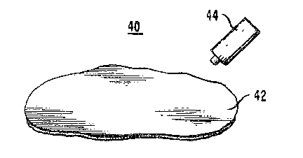
In accordance with the invention, the processing device 40 includes a
10 region of material 42 (see FIG. 3) which exhibits one or more resonant
wavelengths, i.e., the material 42 exhibits an absorption coefficient, ~, greater
than or equal to about 2 x 104 cm~1 at each such wavelength. (For purposes of
the invention, the resonances produced at these wavelengths are associated with
one or more of a variety of material excitations, e.g., electronic excitation,
15 vibrational excitation, etc.) In addition, the device 40 includes one (or more)
sources 44 of electromagnetic radiation to provide one (or more) control beams
at a resonant wavelength or wavelengths. Significantly, both the material 42 as
well as the duration, intensity and resonant wavelength or wavelengths of the
control beam radiation are chosen so as to only populate an energy state or
20 states of the material 42 having decay times less than about 40 ~s, or less than
about 15 ps, or even as small as about 2 ps or less. (Here, the decay time of anenergy state denotes the time interval over which the excited state population
decays to 1/e of its original size.~
If the duration of the control beam radiation is longer than the decay
25 time of an excited state of the material 42, then the excited state will necessarily
be repopulated, resulting in a corresponding, nonlinear optical response having a
duration equal to or longer than that of the radiation. Thus, to achieve a
nonlinear optical response having a decay time, r, as short as the decay time ofthe excited state, the duration of the radiation should be equal to or less than30 t~he decay time of the excited state. (Here r denotes the time interval over
which the magnitude of the nonlinear optical response decreases to l/e of its
original value.)
.
.,
By employing a cycle time (the time interval between applications of the
control beam radiation) equal to (or longer than) about
2 r, it has been found that the resulting resonant, nonlinear optical responses
within the material 42 are essentially free of any relatively slow components
5 even at relatively high repetition rates (the frequency of application of control
beam radiation, equal to the inverse of the cycle time). For example, for the
materials described below, this has been found to be true for repetition rates
higher than about 2.S x 104 Hz (r= 40 ,us), or higher than about 3.3 x 101 Hz
(~= 15 ps), or even as high or higher than about 2.5 x 10¹¹ H~ (r= 2 ps). (For
10 purposes of the invention, a nonlinear optical response in the material 42 isessentially free of any relatively slow component, at a particular repetition rate,
provided that after subjecting the initially unactivated material ~2 to 100 pulses
of control beam radiation at that repetition rate, the nonlinear optical response
produced by the last pulse meets a specific criterion. This criterion is that the
15 ratio of the magnitude of the response maximum (relative to a zero defined bythe unactivated material) to the magnitude of the response after a time interval(subsequent to the one-hundredth pulse) e~ual to the cycle time, is equal to or
greater than about 10.)
Materials exhibiting the relatively short (excited state) decay times,
20 discussed above, are readily found, in accordance with the invention, by
employing a two-step procedure. The first step of this procedure is to find
condensed phase materials, e.g., solid or liquid materials, having absorption
spectra which include resonant wavelengths, as defined above. In this regard,
the absorption spectra of many ~naterials are to be found in a wide variety of
25 references (see, e.g., ~!;~ ~QQk Qii Chem;strv ~ Physics, edited by R. C.
Weast (CR~ Press, Inc~, Boca Raton, Fla.), 60th edition, 1~0), or can readily bemeasured using conventional techniques (regarding these techniques see, e.g.,
P. Las310 and P. Stang, Or~anic Spectroscopv (Harper & Row Publishers,
N. Y.~, 1071). The second step is to vary the resonant wavelength, intensity and30 duration of the control beam radiation until a wavelength-intensity-duration
regime (or regimes) is found which yields an excited state (or states) having the
desired decay time. The presence, and duration, of such excited states is readily
detected using conventional techniques such as time-resolved absorption
spectroacopy or time-resolved luminescence (regarding these techniques, see,
;
.
,
. ,
~2~
- 10-
e.g., "An Apparatus for Obtain;ng Accurate Transient Absorption Spectra on
the Picosecond Time Scale," by R. B. Weisman and B. I. Greene in
~ult;cl~annel Imag~ Detectors, edited by Y. Talmi [American Chemical Society,
Washington, D. C., 1~7~]).
Materials which exhibit resonant wavelengths are typically, although not
exclusively, organic materials. As discussed, one such material is PDA. For
purposes of the invention, PDA is a polymer having the structure shown in
FIG. 4. Here, R denotes any one of a variety of side groups. One such side
group is, for example, paratoluene sulfonate (PTS). Other useful side groups
10 are described in "Structural Aspects of the Topochemical Polymerization of
Diacetylenes," by V. Enkelmann in ~an~ in Po]y.~ Sci~ ~ (Springer-
Verlag, Berlin, Heidelberg, 1984). Significantly, the slde groups play only a
minor role in deflning the optical properties of PDA, typically serving only to
shift the long-wavelength absorption peak of PDA, which is typically located at
15 about 630 nm (see, e.g., FIG. 1 which is the absorption curve for PDA-PTS~.
If, for example, R is PTS, then it has been found, using the procedure
described above, that PDA exhibits both a relatively short-lived electronic
energy state, here denoted S1, and a relatively long-lived electronic triplet state,
here denoted T1. That is, by using 2 ps-long pulses of control beam radiation7
20 it has been found that S1 has a decay time of about 2 ps, and that it alone is
populated at an excitation wavelength of, for example, 625 nm, provided the
control beam intensity is equal to or less than about 4 x 10⁶ W/cm2. On the
other hand, at higher intensities, it has been found that both S1 and T1 are
populated, and that Tl has a decay time of about 40 ~4s.
25 ~ Not only does S1 exhibit a relatively short decay time but, equally
surprisingly, it has been found that the corresponding nonl;near optical response
is much larger in magnitude than previously imagined. For example, when
populating S1 (using the control beam resonant wavelength, duration and
intensit~r, discussed above), signal beam radiation, at the corresponding,
30 resonant wavelength (of 625 nm), will see (what is considered to be) a relatively
large change in refractive index from about 6.0 to about 5.~5. Similarly, such
signal beam radîation will also see a change in absorption coefficient from about
8 x 105 cm~1 to about 7.96 x 105 cm~1, which is correspondingly large.
~IL2~5~
It has been found that populating S1 not only produces a relatively large
change in refractive inde~ or absorption coefi`iciellt in relation to a resonantsignal beam but, quite unexpectedly, produces a relatively large change in
refractive index and absorption coefficient in relation to signal beam radiation5 having nonresonant wavelengths. (The particular nonresonant wavelengths so
affected must generally be determined empirically.)
A variety of optical processing devices 40, capable of operating at
relatively high repetition rates (by virtue of the relatively short decay times of
the material 42), have been developed and are depicted in FIGS. 5-~. ~or
10 example, the device 40 depicted in FI~. 5 is an amplitude modulator. In
operation, a resonant control beam 4~ (emitted by the source 44) is used to
populate a relatively short-lived energy state, to produce a change in absorption.
Simultaneously, a resonant or nonresonant s;gnal beam 22 (emitted by the
source 20) is impinged upon the material 42 to suffer absorption, and thus
15 modulation, i.e., a change in intensity.
The embodiment of the device 40 depicted in FIG. 6 is useful, for
example, as a demultiplexer. In operation, two resonant control beams 46
and 48 (emitted, for example, by two control beam sources~ are interfered on a
surface of the material 4~ (in contrast to a volume region of the material 42), to
20 produce a periodic intensity variation resulting in a periodic variation in
refractive index, and thus a diffraction grating, on the surface of the
material 42. Coincidentally with the formation of the diffraction grating, a
resonant or nonresonant signal beam 22 is impinged upon the surface of the
material 42, and reflectively diffracted from the surface of the material 42. If25 the signal beam radiation 22 consists of a plurality of op$ical pulses which have
been multiplexed onto a waveguide, e g., an optical ~lber, used to communicate
these pulses to the device 40, then selected pulses are readily diffracted, to
achieve demultiplexing, by selectively forming the diffraction grating on the
surface of the material 42. To avoid diffracting non-selected pulse~, the time
30 interval between the pulses should be greater than or equal to the decay time of
the diffraction grating.
A third embodiment of the device 40 is depicted in FI~. 7 and is useful
as a switch. This embodiment includes two intersecting, planar waveguides 47
and 4~. Such waveguides are, for example, thin layers 42 of PDA formed in a
~2~
- 12-
monomeric crystal by subjecting selected surface regions of the crystal to a
beam of energy, e.g., a heat beam or a beam of electrons. (Regarding this
technique for polymerizing PDA from monomeric crystals see, e.g., J. Berrehar,
C. Lapersonne-Meyer and M. Schott, "Polydiacetylene Single Crystal Thin
5 Films," Applied Phvsics T~etters, Vol. 48, No. 10, 1986, pp~ 63~631.) In
operation, two resonant control beams 46 and 48 are interfered on a surface
region of the monomeric crystal common to the two planar waveguides to
produce a diffraction grating. Simultaneously, a resonant or nonresonant signal
beam 22 is propagated down one of the waveguides, e.g., the waveguide 47, to
10 be diffracted (by the diffraction grating), and thus switched, into the other waveguide, e.g., the waveguide 49.
~ fourth embodiment of the device 40, depicted in FIG. 8, is useful as a
modulator. This embodiment includes a planar waveguide 47, e.g., a thin layer
42 of PDA formed in a monomeric, crystalline substrate. In operation, two
15 resonant control beams 46 and 48 are interfered on an upper surface of the
waveguide 47 to produce a periodic variation in refractive index.
Simultaneously, a signal beam 22 is propagated down the waveguide 47. If the
distance, ~L, between adjacent minima in the periodic refractive index variationis equal to half the wavelength of the signal beam radiation (in the waveguide),20 then the periodic variation in refractive index functions as a Bragg reflector,
which reflects the signal beam radiation. Thus, by forming the Bragg reflector
at selected instants in time, the signal beam 22 is modulated, i.e., its intensity is
selectively reduced.
Yet a fifth embodiment of the device 40 is depicted in ~IG. ~, and is also
25 usefully employed as a modulator. This embodiment (which is a variant of the
known Mach-Zender switch) includes a waveguide 45, which bifurcates into
waveguides 47 and 4~ which, in turn, converge to once again form the single
wa~eguide 45. This embodiment also includes a material region 42 (exhibiting a
resonant, nonlinear optical response) overlying one of the waveguides resulting
30 froin the bifurcation, e.g., the waveguide 47. In operation, a signal beam 22 is
propagated down the waveguide 45 (from left to right, as viewed in FIG. ~), and
thus split into two signal beam portions on propagating through the
waveguides 47 and 4~. By impinging the material region 42 with a resonant
control beam 46, a change in refractive index is produced in the material
~l2
- 13-
region 42, which affects the portion of the signal beam 22 propagating through
the underlying waveguide 47. This change in refractive index will necessarily
result in different propagation speeds for the signal beam portions in the
waveguides 47 and 49, resulting in a phase difference between the two beam
S portions at the juncture of the waveguides 47 and 4~. If the refractive index
change is large enough, and is experienced over a long enough path length, then
a phase difference of 7r is readily prodllced. ~s a consequence, the signal beamportions will destructively interfere with one another at the juncture of the
waveguides 47 and ~9, with the resulting, single beam having diminished
10 intensity. Thus, by selectively impinging the material region 42 with the control
beam 46, the signal beam 22 is readily modulated.
As noted above, the GaAs etalon reported by J. L. Jewell et al, supra, is
useful as an optical processing device. However, in addition to its inability toachieve a repetition rate higher than about 3.3x10¹⁰Hz, this device has other
15 limitations. For example, in the absence of control beam radiation, the etalon
exhibits a plurality of transmission peaks, with each peak centered at a
wavelength, ~m, given by the relation
m ~m/2 = nl. (1)
Here, m denotes a positive integer (m = 1,2,3,...), Il denotes the refractive index
20 of the GaAs (prior to being impinged by the control beam), and 1 denotes the
thickness of the C~aAs. Significantly, in the operation of the etalon, the
wavelength of the control beam is chosen so that the corresponding photon
energy is equal to or greater than the bandgap for Ga~s, e.g., the control beam
wavelength is chosen to be 800 nm (as noted above). Consequently, the control
25 beam radiation i~ absorbed, resulting in the formation of electron-hole pairswithin the GaAs. As noted above, the presence of these electron-hole pairs
produces a significant change in the refractive index of the GaAs, but only overa narrow range of wavelengths of electromagnetic radiation, i.e., at room
temperature, the range extends from about 870 nanometers (the wavelength
30 having a corresponding photon energy equal to the bandgap edge in GaAs) to
about 900 nanometers (nm). Thus, by choosing the thickness of the GaAs, 1, so
that one of the etalon transmission peaks lies within the above 30 nm range of
wavelengths, e.g., lies at 8~0 nm (as noted above), then the refractive index
change induced by the control beam serves to produce a corresponding shift in
~1 ~85iifii.~
the wavelength-position of this transmission peak (the shift being calculable
using Eq. (1)). Therefore, if the wavelength of the signal beam is chosen to be
the (initially unshifted) transmission peak wavelength, the subsequent shift in
the transmission peak (induced by the control beam) produces a substantial
5 decrease in the transmission of the signal beam (and a corresponding increase in
the amount of signal beam radiation reflected from the etalon), thus achieving
the desired signal beam processing. However, because the GaAs etalon is
incapable of producing signif~lcant shifts in transmission peaks positioned at
wavelengths greater than about ~00 nm (0.90 ~m), this etalon is incapable of
10 processing signal beams having wavelengths of current commercial significance,
e.g., wavelengths of 1.31,um and 1.55~m, presently favored in optical fiber
communication systems. (In present, commercially available silica optical fibers,
the minimum dispersion wavelength is typically at about 1.31 ~m, while the
minimum loss w3velength is typically at about 1.55 ,um.)
lS Not only is the Ga~ etalon limited in terms of the maximum achievable
repetition rate and in terms of the wavelengths of the signal beams it is capable
of processing, it is also limited in terms of spatial resolution. That is, it has
been proposed that pairs of control and signal beams be simultaneously
impinged upon separate regions of the GaAs etalon to achieve simultaneous,
20 parallel processing of the signal beams. But the electron-hole pairs formed
within each region of the GaAs (as a result of control beam absorption) have a
lifetime of about 20 ns, during which they diffuse as much as about 20 ~m. To
avoid the possibility of cross-talk resulting from the diffusion of electron-hole
pairs from one spatial region of the C~aAs (where a first signal beam is being
25 processed) to a second spatial region (where a second signal beam is being
processed), the dimensions of these spatial regions must be bigger than about 20um, which limits the number of signal beams which can be simultaneously
processed by the etalon.
Yet another limitation of the GaAs etalon is its sensitivity to
30 teinperature. That is, temperature changes produce shifts in the conduction
band edge relative to the valence band of the GaAs. This band edge shift
results in a significant change in refractive index, which has the effect of
shifting all transmission peaks of the etalon, and particularly the transmissionpeak whose wavelength corresponds most closely to the bandgap edge. As a
~12
- 15-
result, the ability of the device to process a signal beam having a wavelength
equal to that of one of the unshifted transmission peaks is degraded.
It has been found that replacing ~aAs with many of the materials 42
useful in the above-described embodiments of the optical processing device 40,
5 results in etalons which overcome the limitations of the (~aAs etalon. That is,
and as noted above, it has been found that many of the materials 42 (exhibiting
resonant, nonlinear optical responses ha~ring decay times less than, for example,
about 40 ,us, or less than about 2 ns, or less than about 15 ps, or equal to or less
than about 2 ps) often also exhibit induced absorptions (having correspondingly
10 short decay times) at other wavelengths. (For purposes of the invention, an
induced absorption is one which is characteri~ed by a substantial change in
absorption per incident absorbed (photon) energy per unit area (a quantity
having the units of, for example, square centimeters per picojoule (cm2/pj)~
and/or a substantial change in refractive index per incident absorbed (photon)
15 energy per unit area (al30 having the units of, for example, cm2/pj). In thisregard, for purposes of the invention, a substantial change in absorption per
incident absorbed (photon) energy per unit area is one which, in absolute terms,is equal to or greater than about 103cm2/pj, while a substantial change in
refractive index per incident absorbed (photon) energy is one which, in absolute20 terms, is equal to or greater than about 10 cm2/pj.) In addition, it has beenfound that many of the materials 42 also exhibit substantial nonlinear optical
responses at nonresonant wavelengths, which also have decay times less than,
for example, about 40 ~s, or less than about 2 ns, or less than about 15 ps, or
equal to or less than about 2 ps, and which also lead to the same type of
2S ~induced absorptions (having correspondingly short decay times), discussed
above. (For purposes for the invention, a material exhibits a substantial
nonlinear optical response at a nonresonant wavelength if the absorption
coefficient, ~, at that wavelength is less than about 2 x 104 cm~l but greater
than or equal to about 1 x 103cm 1.) Moreover, it has been found, in many
30 instances, that the wavelengths at which the induced absorptions occur are
often higher than about 0.~0 ~4m, that the induced absorptions often extend
over wavelength ranges larger than about 30 nm, and that the induced-
absorption wavelengths often include commerciaily significant wavelengths.
~s~
- 16-
If material 42 exhibiting induced absorptions of the type described above,
at one or more wavelengths, is employed in an etalon, if the induced absorptionslead primarily to, for example, substantial increases in absorption per incidentabsorbed (photon) energy per unit area, and if the thickness of the etalon i8
5 chosen to produce etalon transmission peaks at the induced-absorption
wavelengths, then impinging a (resonant- or nonresonant-wavelength) control
beam upon such an etalon will necessarily produce significant increases in
absorption at the induced-absorption wavelengths, and consequently produce
substantial reductions in the magnitudes OI the transmission peaks. Thus, if
10 the signal beam impinging the etalon has a wavelength equal to that of one ofthe etalon transmission peaks, the signal beam will suffer substaDtially reducedtransmission through, and a corresponding increase in reflection from, the
etalon when the etalon is impinged by the control beam, resulting in the
processing of the signal beam. As discussed more fully below, the material 42
15 and control beam are readily chosen so as to permit the processing of a signal
beam having a wavelength greater than 0.90 ,um, e.g., 1.31 ~m or 1.5S ~m,
which is not possible with the Ga~s etalon. In addition, if the nonlinear optical
response, and the induced absorption, of the material 42 have decay times
smaller than about 15 ps ~materials exhibiting such decay times are readily
20 found, as described below), then the etalon will be operable at repetition rates
higher than about 3.3 x 101 Hz, which is also not achievable with the ~aAs
etalon.
Materials ~2 exhibiting both a nonlinear optical response, i.e., a resonant,
nonlinear optical response and/or a substantial nonlinear optical response at a
25 nonresonant wavelength, and an associated induced absorption at a wavelength
greater than, for example, about 0.90 ~m and/or extendin~ over a wavelength
range greater than about 30 nm, with the nonlinear optical response and
induced absorption having the relatively short decay times, discussed above, arereadily found using the two-step procedure, described above. That is, during
30 thë first step, condensed phase materials are sought having absorption spectra
which include resonant wavelengths and/or nonresonant wavelengths exhibiting
substantial, nonlinear optical responses. Then, during the second step, the
wavelength, intensity and duration of the control beam radiation are varied
until a wavelength-intensity-duration regime (or regimes) is found which yields a
-- .
~2~
- 17 -
resonant or nonresonant, nonlinear optical response and an induced absorption
at a desired wavelength or wavelengths, having the desired decay time. The
presence, and duration, of the resonant or nonresonant, nonlinear optical
response and induced absorptions are readily detected using, for example, the
5 conventional technique of time-resolved absorption spectroscopy (see, e.g., R. B.
Weisman and B. I. Greene, supra).
Using the above procedure, it has been found, in the case of, for example,
PDA-PTS, that a single excited state, which decays to the ground state (via a
relatively short-lived intermediate state) over a decay time of about 2 ps, is
10 readily populated by using a control beam pulse having a resonant wavelength
of 0.64 ,um, a duration of 0.2 ps (full-width-at-half-maximum~ and an intensity
(the ratio of pulse energy to pulse width, per unit area) of 5 x 10⁸ W/cm2.
Moreover, populating this excited state results in induced absorptions,
characterized primarily by substantial increases in absorption per incident
15 absorbed (photon) energy per unit area, at virtually all wavelengths extending
from about 0.7 ,um up to at least 1.7 ~m, including the wavelengths of 1.31 ~m
and 1.55 ,um, and exhibiting decay times of about 0.~ ps. (The e}~istence of
these induced absorptions has only been measured up to 1.7 ~m, and may also
exist at higher wavelengths.) Thus, an etalon containing PDA-PTS permits
20 optical processing of signal beam radiation having wavelengths currently favored
in optical fiber communication systems, permits signal beam processing
extending over a range of wavelengths much greater than 30 nm9 and at
repetition rates of, for example, 2.5 x 10¹¹ Hz.
If the material 42 is chosen to exhibit, for example, an excited state and
; 25 an induced absorption ha~ring a decay time less than that of the electron-hole
pairs produced in GaAs, i.e., a decay time less than about 15 ps, and if the rate
of transfer o~ the energy associated with the excitation in the material 42 is
similar to the electron-hole diffusion rate in GaAs, then this energy (associated
with the excitation in the material 42) will be propagated over a distance,
30 during the relatively short decay time of the excited state and induced
absorption, which is smaller than the distance traversed by the electron-hole
pairs in GaA~ during their longer decay time. As a consequence, an etalon
employing such a material 42 will be capable of overcoming yet another
limitation of the ~aAs etalon, i.e., it will be capable of simultaneously
~s~
- 18-
processing more signal beams than an equally-sized (~aAs etalon.
As noted above, the materials 42 are typically (although not exclusively)
organic materials, rather than inorganic semiconductor materials, as is the casewith GaAs. Significantly, it has been found that the performance of etalons
5 employing organic materials is not nearly as sensitive to temperature
fluctuations as is the performance of etalons employing ~aAs.
As a result of the above findings, a new embodiment of the optical
processing device 40 has been developed, useful in the above-described optical
system 10. This new embodiment is depicted in FIG. 13 and includes an etalon
10 70, as well as a source 44 (see FIG. 3) of control beam radiation 46. The etalon
70 includes a material region 42 sandwiched between two material regions 64
having inwardly-facing (as viewed in FIG. 13), mirror-like surfaces 66. The
material region 42 is chosen to exhibit a resonant, nonlinear optical response
and/or a substantial nonlinear optical response at a nonresonant wavelength,
15 and an associated, induced absorption, at one or more wavelengths, having the relatively short decay times, discussed above. Preferably, this induced
absorption is at a wavelength greater than about 0.90 ~m and/or extends over a
wavelength range greater than about 30 nm.
Each of the two material regions 64, which typically include dielectric
20 materials such as magnesium fluoride or zinc sulfide, has both an inwardly
facing surface 66 and an outwardly facing surface 68. Significantly, the two
outwardly facing surfaces 68 are designed to exhibit relatively low reflectivity to
both the control beam 46 and signal beam 22, i.e., the surfaces 68 are designed
to reflect less than about 5 percent of impinging electromagnetic radiation at
25 the control beam and signal beam wavelengths (to permit the control and signal
beams to penetrate into the interior of the etalon). This relatively low
reflectivity is achieved, for example, by applying conventional (single-layer)
anti-reflection coatings to the surfaces 68. In addition, at least one of the inner
surfaces 66, i.e., the surface 66 initially impinged by the control beam, is
30 designed to exhibit relatively low reflectivity (as defined above) to
electromagnetic radiation at the control beam wavelength, while both inner
surfaces are also designed to exhibit relatively high reflectivity (i.e., a reflectivity
greater than about 50 percent) to electromagnetic radiation at the signal beam
wavelength. This difference in reflectivities at the two wavelengths is achieved,
~2~
- 19 -
for example, by applying conventional multi-layered coatings to the surfaces 66. During the operation of the etalon 70, the wavelength of the signal beam
22 must necessarily be equal to one of the induced-absorption wavelengths.
Thus, the thickness of the material region 42 is chosen to produce an etalon
5 transmission peak at this particular induced-absorption wa~elength. In general,
the thickness of the material region 42 is preferably less than about 50 ,um.
Thicknesses greater than about 50 ,~4m, while not precluded, are less desirable
because they lead to relatively low device contrast ratios.
Signirlcantly, the etalon depicted in FIG. 13 is useful in achieving
10 amplitude modulation, as well as time-division and wavelength-division
multiplexing and demultiplexing. For example, in the event that a single signal
beam 22 is to be modulated, then selectively impinging the etalon with the
control beam 46 will produce a shift and/or change in amplitude of the
transmission peak initially centered at a wavelength equal to the signal beam
15 wavelength, selectively reducing the transmission of the signal beam through
the etalon, and thus achieving the desired amplitude modulation. In addition, ifa single, unmodulated signal beam, e.g., a constant intensity signal beam,
having a wavelength equal to that of one of the etalon transmission peaks, is
impinged upon the etalon, and if the etalon is also impinged by two or more
20 modulated, i.e., information-containing, control beams 46, then the information
contained in the control beams will be impressed upon the originally
unmodulated single beam, resulting in the creation of a time-division
multiplexed signal beam. Similarly, if the material 42 exhibits induced
absorptions at two or more wa~elengths, if the etalon has transmission peaks at
25 these wavelengths, and if the etalon is impinged by a single, unmodulated signal
beam having wavelengths encompassing the etalon transmission peaks, then
impinging the etalon with two or more information-containing control beams 46
will transmform the single, unmodulated signal beam into a wavelength-division
multiplexed signal beam. On the other hand, if the etalon is impinged by a
30 time-division or wavelength-division multiplexed signal beam, then selectively
impinging the etalon with one or more control beams 46 will result in one or
more signal beams, contained within the time-division or wavelength-division,
multiplexed signal beam being selectively re~lected from the etalon, thus
achieving demultiplexing.
.
- 20-
~1
An irregularly shaped sample of PDA-PTS, having length and width
dimensions of about 1 centimeter (cm), and a thickness of about
2 millimeters (mm), was formed by thermally polymerizing a monomer crystal,
5 using the technique described in J. Berrehar et al., supra. This sample included
a naturally occurring facet (a surface) which contained the b axis of the crystal
(i.e., the b axis was parallel to the plane defined by the facet), and had length
and width dimensions of about 1 cm.
A single amplified, colliding pulse modelocked (CPM) dye laser was used
10 to produce both the signal and control beam optical pulses impinged upon the
PDA-PTS facet. The laser produced light pulses at a repetition rate of 10 Hz, ofwavelength centered at 625 nm (FWHM 7nm), of duration equal to
70 femtoseconds, and having energies of 400 microjoules per pulse. In operation,each optical pulse emitted by the laser was split (using a conventional beam
15 splitter) into two pulses, i.e., a signal beam pulse and a control beam pulse, and
one of the pulses (the signal beam pulse) was variably delayed (using a
conventional optical delay line~ relative to the other pulse (the control beam
pulse).
The control beam pulses emitted by the laser were focused (using a
20 conventional lens) onto the PDA-PTS facet to a spot size having a diameter ofabout 1 mm. Prior to being focused, each control beam pulse was variably
attenuated, using conventional neutral density filters, to vary the control beamintensity. In addition, each control beam pulse was passed through a polarizer
to achieve a control beam polarization parallel to the b axis of the crystal.
25 ~ Each signal beam pulse was focused (using a conventional lens) into a
water-containing cuvette, having a 3 cm-long optical path length, to achieve
continuum generation, i.e., to produce a spectrally broadened laser pulse of
essentially unchanged duration ( 70 femtoseconds). The resulting continuum
pulse was then passed through a spectral notch f~llter, centered (in wavelength)30 at 625 nm (with a FWHM of 9 nm), to select out the desired wavelengths. The
spectrally filtered pulse was then passed through neutral density filters to
achieve a signal beam pulse intensity less than the corresponding control beam
pulse intensity. In addition, each signal beam pulse was passed through a
polarizer to achieve a signal beam polarization identical to the control beam
polarization. The resulting signal beam pulse was then focused (using a
conventional lens) onto the facet, to the same spot as the control beam pulse.
A conventional 50/50 beam splitter was placed in the path of the signal
beam to redirect a portion of the signal beam radiation away from the facet and
S onto a first, silicon photodiode detector. The remainder of the signal beam
radiation was impinged upon the facet, reflected, and detected by a second,
silicon photodiode detector.
The signals produced by the two detectors were subtracted from each
other to produce a resultant s;gnal. In the absence of the control beam pulse,
10 there was no change in the magnitude of the resultant signal. However, when
the control beam pulse was impinged upon the facet, a change in reflectivity,
~R, was produced via the resonant, nonlinear optical response, which resulted
in a change in magnitude of the resultant signal.
The temporal component or components of the resonant, nonlinear
15 optical response induced in the PDA-PTS was mapped by measuring, and
plotting, ~R as a function of delay time for different delay times and differentcontrol beam pulse intensities. Such a plot is shown in FIG. 10, for the case
where the control beam pulse intensity was equal to 101 W/cm2. Analysis of
this plot indicates the existence of a first, relatively short-lived temporal
20 component, having a decay time of about 2.0 ps, and a second, much longer-
lived temporal component.
Reducing the intensity of $he control beam pulse yielded a reduced
(compared to the signal shown in FIG. 10) resultant signal. Significantly, the
second temporal component was more reduced than -the first.
25 E~l~ ~
The PDA-PTS sample, described above, was again subjected to signal
and control beam pulses, with the signal beam pulses being variably delayed, as
described above. However, and prior to being impinged upon the sample, each
control beam pulse was split into two pulses by a conventional S0/50 beam
30 spiitter. The split control beam pulses then traversed paths of identical length
prior to being recombined, via mirrors, at the surface of the facet. These
recombined pulses, which met at an angle of about 16 degrees, interfered with
each other at the facet surface to produce a periodic intensity pattern which,
via the resonant nonlinear optical response, served to reflectively diffract the
~2~
- 22-
portion of the signal beam pulse incident on the facet.
Rather than subtracting the signals produced by the two detectors from
each other, the two signals were ratioed (the ratio of the detector signal
produced by the diffracted portion of the signal beam pulse to the detector
5 signal produced by the redirected portion of the signal beam pulse) to produce a
resultant signal. One such resultant signal, for the case where the interfering
control beam pulses had intensities of 6 x 10⁹ W/cm2, is shown in FI~. 11.
Analysis indicates that this resultant signal includes both the relatively short-
lived and long-lived temporal components, discussed above. Reducing the
10 intensities of the interfering control beam pulses to 6 x 10⁸ W/cm2 yielded the
resultant signal shown in FIG. 12. Here, analysis indicates that essentially only
the relatively short-lived temporal component is present.
E~l~ 3
A PD~-PTS single crystal f~llm, having a thickness of about 1.7 ~m, was
15 grown using the technique described by M. Thakur and S. ~Ieyler in, "~rowth
Of Large-Area Thin-Film Single Crystals Of Poly (diacetylenes)",
Macromolecules, Vol. 18, p. 2341, 1~85.
The transient-absorption spectroscopy technique described by
R. B. Weisman and B. I. Greene, supra, was used to detect induced absorptions
20 in the PDA-PTS. That is, a single, colliding pulse modelocked (CPM) dye laserwas used to produce optical pulses having wavelengths of 630 nm and durations
of 200 femtoseconds. These pulses were amplified by a neodymium-YAG
pumped dye laser/amplifier to achieve pulse energies of 500 microjoules. Each
(amplified) optical pulse generated by the CPM laser was split (using a
25 conventional beam splitter) into two pulses, i.e., a signal beam pulse and a
control beam pulse. One of these pulses (the signal beam pulse) was variably
delayed (using a conventional optical delay line) relative to the other pulse (the
control beam pulse), prior to both pulses being impinged upon the PDA-PTS, to
probe the temporal response OI the PDA-PTS. ~oth the control and signal
30 beam spot sizes at the surface of the PDA-PTS were about 1 mm in diameter,
- and the control beam pulse energy, at the PDA-PTS surface, was about 1
microjule. (~onventional photodiodes were used to detect the signal beam pulses
tran-mitted by the PDA-PTS.
.
- :~
.
.
- 23-
Each signal and control beam pulse was also subjected to the continuum
generation technique, described in ~xample 1, to achieve spectrally broadened
pulses, i.e., optical pulses having wavelengths ranging from about 0.4 ~m to
about 1.7 ,um. However, the spectrally broadened control beam pulses were
5 passed through a spectral notch filter which only transmitted light at 640
(~t5)nm, thus yielding control beam pulses having wavelengths of 640 nm.
Thus, the temporal response of the PDA-PTS, at (signal beam) wavelengths
ranging from about 0.4 ,um to about 1.7 ,um, was measured.
The results of the above spectroscopy technique clearly indicated the
10 presence of induced absorptions within the PDA-PTS (in response to the control
beam pulse), extending in wavelength from about 0.7 ,um to about 1.7 ~m, and
having decay times of about 0.8 ps.
Example 4
An etalon was fabricated by using optical cement to adhere the PDA-
15 PTS film of Example 3 to two dielectrically-coated mirrors, purchased from the
CVI Corporation of Albuquerque, New Mexico. These mirrors were specifically
designed to be ~5 percent reflecting to 0.96 ~m light (but were also 95 percent
reflecting to 1.0 ~l4m light) and more than 85 percent transmissive to 0.64 ,um
light.
The transient-absorption spectroscopy technique of Example 3 was used
to obtain the temporal response of the etalon, for different signal beam
wavelengths, as a function of the delay time between the control and signal
beam pulses. One such temporal record is displayed in FIG. 14, and
corresponds to the case where the signal beam spot size was about 25 ,um, the
25 control beam spot size was about 100 ~m, and the control beam pulse energy
was about 8 nanojoules. This record shows a transient change in the
transmission of the etalon at a wavelength of about 1.0 ,um (a transmission peakof the etalon). The record also indicates that the transient change had a decay
~:me ~r about l ps.