Note: Descriptions are shown in the official language in which they were submitted.
~2~5~fl.~
-- 1 --
GPTICAL SWITCHING DEVICES
BT PATENTS CASE A23571 (0419P) SUBS
This invention relates to optical switching devices
iand in particular devices which switch the orientation of
a liquid crystal as the primary control mechanism.
Many configurations have been proposed for optical
switching devices which include one or more path regions
for optical signals, said path regions being adjacent to a
liquid crystal region which is comprised in the confining
o region of the path or in a common confining region of two
or more paths. The liquid crystal is associated with
electrodes and the application of control voltages
actuates the device.
The mode of operation of these cptical switches is as
~ollows. The change in the electrical state of ~he
electrodes, usually between "field on" and "field off",
affects the state o~ the liquid crystal and in particular
changes its refractive index whereby the e~fect of the
confining region is substantially altered.
In dsvices with a single path region, usually called
"blocking switches", the change makes the difference
~'i between confining the radiation in the path region and
allowing it to esciape, ie. an "on-off" switch. There are
also "coupler devices" in which the liquid crystal
~, 25 separates two path regions and the change in refractive
index makes the di~ference between permitting or
I
preventing exchange of energy between the two paths.
i ~ Although many con~igurations have been proposed, they
all share a common problem. This arises from the inherent
.j 30 uniaxiality of the nematic liquid crystal phase. In a
j~jj uniaxial material there is only one direction in which
~j
light can propagate and all directions 'see' the same
' :
:
.:
5~
- 2 ~
refractive index. In all other directions, different
polarisations are di~ferently affected, le the devices are
polarisation sensitive. This reduces the switch efficacy
as only one polarisation can be affected at each switch.
For polarisation independence, two directions are required
where the input light sees the same index for all
polarisations. In these two directions the index must be
different from the other direction. Thus the ~abrication
o~ liquid crystal devices poses the problem of reducing
o the polarisation sensitivity, preferably to make an
intensity di~ference of at least lOdB in the switched
signals.
The problem is solved by providing a liquid crystal
control region such that, in at least one of its
configurations9 its molecules adopt a splayed
configuration. For example, the molecules may be arranged
in a ~an configuration.
It is convenient to configure the device so that the
splayed configuration is adopted when the control voltage
is "off" and for the splayed ccnfiguration to correspond
to the lloff'l state of the optical device.
The major factors necessary to understand the mode o~
operation of an optical switching device according to the
invention include the following:
(1) Re~ractive Index
The molecules of the liquid crystal composition
are much longer in one direction, conveniently called the
molecular axis, than in other directions. I~ all the
molecules were aligned with their molecular axes parallel,
the liquid crystal would have an extraordinary refractive
index; that is the refractive index would be greater in
the direction of molecular orientiation than in other
dlrections.
.
-- 3 --
(2) Dipole Moment
The molecules all have a dipole moment and it is the
interaction of this dipole moment with an applied electric
field which actuates the device. When the dipole moment
is perpendicular to the molecular axis the liquid cyrstal
is said to have negative dielectric anisotropy,
conveniently abreviated to N M. When the dipole moment is
parallel to the molecular axis the crystal has positive
dielectric anisotropy, conveniently abbreviated to PDAo
lo (3) Electric Field
When an electric field is applied the dipole moments
attempt to align themselves parallel to the ~ield. Thus
the molecules of NDA liquid crystals align their axes
perpendicular to an applied field whereas the molecules of
PDA l~quid crystalis align their axes in the same
direction as the field. Since it is geometrically more
convenient to orientate electrodes parailel to path
regions they apply fields perpendicular to the path
regions. Thus devices with NDA liquid crystals are "off"
when the field is "off" and vice versa whereas devices
with PDA liquid crystals are "off~ when the field is "on"
and vice versa.
In the "of~" state it is necessary to provide a
splayed orientation, ie to cause different orientations of
the molecules and, therefore, PDA devices require "bent"
or directionally non-uniform electric fields (which are
conveniently provided by non,planar electrodes).
(4) Surface Treatments
The orientation of the molecules is also a~fected by
chemical treatments applied to the surfaces with which the
liquid crystal is in contact. Homeotropic ~reatment, or
HT, gives a preferred orientation wherein the molecular
axis is normal to the sur~ace whereas homogenous
treatment, or HG, gives a preferred orientation wherein
the molecular axis is parallel to the surface. The
surface treatment is critical for a liquid crystal device
si~ce the chemical forces it imposes are an essential part
of the control mechanism.
The surfaces to which the treatment is applied are
usually parallel to the path directionO
Thus HT treatments cause molecules to become normal to
the path regions; ie an "off" configuration when the
lo electric field is "off". Therefore HT treatment is
usually used in conjunction with NDA liquid crystals. The
control surface should have different orientations eg
surround the liquid crystal, to provide the "splay" needed
for polarisation insensitivity.
H~ treatments also require the surface to be rubbed
and the molecules tend to align themselves with the
rubbing direction. Thus rubbing the control surface
parallel to the path regions produces an "on"
configuration when the field is "off". Therefore HG
treatments are usually used in conjunction with PDA liquid
crystals.
(Because rubbed alignments are difficult at the small
scale of the devices, HT treatments with NDA materials
attract most interest).
; 25 Thus the liquid crystal is affected by a combination
of the forces identi~ied in both (3) and (4) above when
the electric field is applied but only by the forces
described in (4) above when no field is applied. The
difference in configurations under these two different
circumstances provides the difference of refractive index
which actuates the device. In one configuration the
molecules are caused to adopt a configuration normal to
the path region and in this configuration the molecules
must be su~ficiently splayed to avoid unacceptable
polarisation sensitivity.
~L2~
We have found that good polarisation insensitivity
is achieved in device configurations in which the liquid
crystal zone is surrounded by a peripheral wall which exerts
the chemical control. For example the whole of the
peripheral wall is provided with the same control treatment,
e.g. all homeotropic. Homeotropic treatments are convenient
to apply because they merely involve dipping and drying.
The peripheral wall can be regard~d as a tubular
surface which contains the liquid crystal. Electrodes and
optical interfaces constitute segments of the peripheral
wall.
The invention is defined in the claims.
The switching efficacy at an output port is
measured by the ratio of the two outputs for the two states
of the switch for the same input. If the efficacy of the
switch is too low detectors in the output circuit (which
dectors could be at long distance) could have unacceptably
high error rates. Thus it is necessary to have switching
efficacies about lO dB, preferably above 15 dB, to achieve
good error rates in the switched output. While very high
switching efficacies are desirable it is believed that at 30
dB (or higher) the error rate properly attributable to
imperfect switching performance is negligible.
The invention will now be described with reference
to the accompanying drawings in which:
Figure 1, shows idealised molecular orientations
for giving polarisation insensitive "on" and "off" states,
Figure 2, shows a molecular orientation probably
associated with the alleged "on" and "off" states of a
conventional configuration;
~` Figure 3, shows a molecular orientation which is
believed to offer an improvement to the ~'o~f" state
; illustrated in Figure 2
Figure 4, is a transverse cross-section
; 35 illustrating a conventional liquid crystal blocking switch;
Figures 5-8, are transverse cross-sections
illustrating blocking switches according to the invention;
~ 3~
Figures 9 and 10, are transverse cross-sections
illustrating couplers according to the invention. The
couplers use NDA material and HT treatments;
Figures 11-13, illustrate the operative parts of
a coupler according to the invention, namely the path
regions, liquid crystal and the electrodes. The couplers
use NDA material and HT treatments;
Figures 14-16, illustrate a way of assembling a
device as shown in Figure 10; and
Figure 17, illustrates a coupler according to the
invention. It uses PDA material and HG treatment.
The invention will now be further described with
reference to the accompanying drawings in which Figures 1-3
are diagrams to assist with theoretical explanations and
Figures 5-13 illustrate exemplary devices according to the
inventions.
We wish to establish that while we believa our
theoretical explanations may provide a use~ul insight into
the mode o~ operation, at least until better theories are
developed, we do not guarantee that the theories are
correct.
In addition to theoretical discussion, we also
provide a disclosure of operational techniques which we
believe to be clear enough and complete enough to enable a
person skilled in the art to produce polarization
insensitive devices.
In all figures the path regions are approximately
cylindrical and normal to the page. Preferably path
regions, numbered 10 in the drawings, are implemented in
sio2 doped with GeO2 and invariant confining regions, 11 in
the drawings, are implemented in undoped sio2.
In Figures 2 to 13, the path region 10 i5 partly
enclosed by an invariant confining region 11. As is
conventional, the con~ining region includes a liquid crystal
neighbourhood 12. Electrodes 13 and 15, which locate and
control the liquid crystal neighbourhood 12, are shown in
Figures 4 to 13 and 16.
, ~ ~
~.,i..~.~
: .
Figure 1 shows what would be an ideal structure if
it could be achieved in practice. The path region 10 is
completely surrounded by the liquid crystal 12 and in the
"off" configuration all the molecules 13 are orientated
radially. In the 'lon" configuration the molecules are
orientated parallel to the direction of propagation, i.e.
normal to the page.
The configuration so identified in Figure 1 is
"off" because the extraordinary direction of the liquid
crystal is, at all locations, normal to the direction of
propagation and therefore all polarizations of radiation are
controlled by th~ high extraordinary refractive index which
gives an "off" state. In the "on" configuration all the
molecules are aligned with the direction of propagation so
that all polarizations of radiation are controlled by the
low ordinary refractive index which gives an "on" state.
It should be noted that both "on'l and "off" states
are cylindrically symmetrical so all polarisations are
;~
.~ . "
~1.2~
affected by the same environment, ie. such a device would
be polarisation insensitive. However, it is di~ficult to
locate electrodes so as to control a liquid crystal which
surrounds the path region 109 and, therefore other
configurations need to be considered.
Figure 2 shows a more practical con~iguration in which
the path region 10 is partially enclosed by an invariant
con~ining region 11 which does not participate in the
swltching function. The regions 10 and 11 have a flat
o optical interface 14 which is in contact with the liquid
crystal 12.
The "on" configuration is similar to Figure 1 in that
the molecules are aligned parallel to the direction o~
propagation but there is an important difference in the
"off" configuration because the molecules are orientated
normal to the interface 14 ~instead of radially).
For convenience of explanation, rectangular axes OY
(normal to both optical interface 14 and the direction of
propagation) and OX (parallel to interface 14 and normal
to the direction of propagation) are shown in Figure 2.
In the "off" stage of Figure 2 the molecules are all
aligned ~n the direction OY. Thus radiation polarised in
the direction OY is controlled by the extraordinary
refractive index and, therefore, it passes through optical
interf~ce 14 and it is not prqpagated. However, radiation
polarised in the direction OX is controlled by the
ordinary re~ractive index which is selected so as to
provide the "on" configuration. Thus the alleged "off"
state is only "off" to scme polarisations. It is
suggested that there is a critical direction, shown as OA
in Figure 2, for which the effective index is equal to the
critical value separating the "on" state from the "off"
state. Thus polarisations in the angle AOX are "on" and
' .
only polarisations in the angle AOY are "o~f". It is thus
proposed that, because the liquid crystal is too strongly
orientated in the OY direction there cannot be both
satis~actory "on" and "off" states.
Figure 3 illustrakes a mechanism which is believed to
contribute to polarisation insensitivity. Instead of all
the molecules being orientated in the direction OY they
are splayed, ie. in a fan configuration with a variety of
angles to the normal. This reduces the refractive ~ndex
lo for polarisation in the OY direction but the value is
still high enough to provide an "off~ state. However, the
splay also increases the refractive index in the OX
direction whereby an "off" state in this direction bec~mes
possible.
The (conventional) configuration shown in Figure 4
comprises a half coupler block 20 having a confining
region 11 and a path region lO. An electrode 13 is
provided on the face of the half coupler block 20 and a
liquid crystal 12 is located between electrode 13 and a
second electrode 15. The surface of both electrodes are
HT-treated and this treatment causes the molecules to
align themselves normal to the interface surface as
indicated by the dotted lines. Thus the device operates
an indicated in Figure 2 and its lloff" state is
unsatisfactory.
Some specific configurations of devices according to
the invention will now be described.
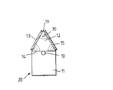
Figure 5 shows a blocking switch which comprises a
half-co4pler block 20 having a confining region ll and a
path region lO adjacent to an optical interface surface
14. An NDA liquid crystal region 12 is in contact with
optical inter~ace surface 14 and it has a triangular cross
section. The other sides of the triangle are formed by
-
-- 10 --
electrodes 13 and 15 which are electrically separated by
an insulating segment 19. All these surfaces, ie. both
electrodes 13/15 and surfaces 14/19, were HT-treated
before assembly. This provides the splayed configuration
in the ~off" state
The device shown in Figure 6 also utilises an NDA
liquid crystal 12 and surfaces 1~/14/15/19 were
HT-treated. It provides a good "on" state when an
electric field is applied across electrodes 13/15 and a
o good lloffl' state when no field is applied. Both of these
states are substantially independant of the polarisation
of the signals in path 10. The theory given above
explains this observation as follows.
In the "off" state the molecules try to stand normally
to all three surfaces because each surface has been
HT-treated, the result is that the molecules of the liquid
crystals try to orientate themselves along the dotted
lines 30 shown in Figure 5. This is a splayed arrangement
and, therefore, the "off" state is polarisation
insensitive
When an electric field is applied to electrsdes 1~/15
the molecules attempt to align themselves normal to the
ield, ie. parallel to the path 12. However the ef~ects
of the surface treatment will still be felt and any
non-alignment will be splayed whereby the llon" state is
also polarisation insensitive.
There is an important difference between Figures 4 and
5 in that Figure 4 has the electrodes 13/15 parallel and
the chemical forces due to the surface treatment cause
j 30 substantial orientation of the molecules normal to
interface. This causes polarisation sensitivity.
In the conventional device of Figure 4, the electrode
:`~
: .
'~
13 intrudes into the optical system whereas devices
according to our invent~on have the electrodes 13/15
located outside the optical system.
Figures 7 and 8 correspond to Figures 5 and 6 with the
further dif~erences that the surfaces 13/14/15/17 were HG
treated and the liquid crystal is of the PDA type. There
is also the difference that the lines 31 represent a
nbent" electric field instead of chemical forces. Figures
7 and 8 will be discussed further below.
o Figure 9 illustrates a device which includes two
half-coupler blocks 2u^A and 20B with two path regions lOA
and lOB. The electrodes 1~ and 15 take the ~orm of
conductor wires located between blocks ~OA and 20B. The
wires and the path regions all have similar dimensions.
All the surfaces are HT-treated and this causes the
molecules to adopt a splayed orientation whereby the
device is polarisation insensitive.
With two paths (as shown) the device is a switchable
coupler. With the electric fleld "on~ energy will
'transfer from path A to path B via optical interfaees
14A/14B (or B to A if desired) but with the ~ield "of~"
; the energy will be confined to its own path.
Energy should be supplied into only one of the paths,
ie. there is only one input, and because the device is
polarisation insensitive one output path will have a very
low intensity with a relatively high intensity in the
other.
- Figure 10 is a modified ~ersion of Figure 9 in which
the liquid crystal region has a square con~iguration.
Arrangements of the liquid crystal 12 in relation to
paths lOA and lOB and also electrodes 13 and 15 are shown
in Figures 11, 1~ and 13. In all these drawings the
direction of molecular orientation is indicated by the
:
- 12 -
dotted lines ~0. Figure 12A and 12B illustrate concave
electrodes whereas Figures 13A and 13B illustrate convex
electrodcs.
There is a common feature in Figures 11-13 in that in
its cross section normal to the paths lOA and lOB, the
liquid crystal 12 is surrounded by a peripheral HT treated
surface. Thus the outer layer of molecules is orientated
inwards, ie. normal to the surrounding surface, and thus
the splayed orientation associated with polarisation
lo insensitivity is produced.
This sur~ace effect only extends into the crystal
volume for a short distance, eg. up to about 25 microns,
so the maximu~ dimension for the liquid crystal region 12
is about 30 microns (diameter). Locating electrodes 13
and 15 within this distance minimises the voltages needed
to operate the device. The diameter of paths lOA and lOB
is usually about 8 microns (for optical reasons) and this
is about the minimum size for the liquid crystal zone.
The paths lOA and lOB are correctianally not more than 10
micrometres, eg about 1-2 micrometres behind the
interfaces 14A and 14B. Figures 11-13 are based on these
size relationships.
It should be noted that energy transfer takes place
via optical interfaces 14A/148, ie. the optical path is
lOA, 14A, 12, 14B, lOB and the electrodes l3/15 do not
obtrude into thls path. Also any configuration suitable
for use as a coupler can be used for a blocking switch by
omitting (or not connecting) one of the paths.
The assembly of a device as shown in Figure 10 (and
11) Will be briefly described.
The starting point shown in Figure 14, was two glass
rods 40A and 40B, prepared by oonventional inside
deposition, (MCVD), w1th cores lOA/lOB of GeO2 doped
~::
' '
'
.
- 13 -
silica and claddings llA/118 of undoped silica. The
shaded regions 41At41B were ground away to give preforms
~or half coupler blocks 2~A and 2C3. As is conventional
for glass ~ibre the preforms were drawn to reduce the
cross-sectional dimension to those of the ~inished device
and surfaces 13, 15, see Figure 15, were metallised to
give precursors of electrodes 13, 15. This drawing and
- - metallisation converted the rod 40A and 40B into half
coupler blocks.
lo ~fter metallisation the two half coupler blocks were
HT-treated. This comprised immersion for a few seconds in
a solution of cetyl-trimethyl-ammonium bromide in
isopropyl alcohol (0.1 gm per 100 mls). On removal from
the solution the half coupler blocks were dried at
lW Cl and cut into lengths of 1 to 10 cm. This gave a
set of half coupler blocks 20A and another set of hal~
coupler blocks 20B.
An item from each set were juxtaposed as shown in
Figure 16 and molten liquid crystal composition was
allowed to wick into capilliary bore 50. The liquid
crystal composition was allowed to cool giving a device as
shown in Figure 10.
The liquid crystal composition was a mixture of two
compounds each with the generic formula:-
CH3(CH2)nc6Hlo-co-o-c6Hlo(cH2~mcH3 .
wherein C6Hlo represents a cyclohexane residue in the
all-trans configuration and having two substituents in the
para positions.
The mixture consisted of:-
mole% n m
6~ 2 2
4 - 2
,
'i '
, ~'
~2~
- 14 -
The e~ficiency of the swi$ch was assessed by measuring
the ratio o~ the intensities o~ output with the voltage
"on" and "o~f". The ratio was 15 dB and this implies that
all polarisations of light were switched.
Figure 17, in which the operative parts are arranged
in a configuration similar to Figure 13A, illustrates a
device according to the invention us~ng a PDA material as
liquid crystal 12. The surfaces of the electrodes 13 and
15 and the interfaces 14A and 14B are all HG treated and
o rubbed parallel to the path regions lOA and lOB; in other
words the rubbing was normal to the page. The dotted
lines 31 indicate the direction of the electric field when
the electrodes 13, 15 are charged. It is e~phasised that
the field lines 31 are bent because the electrodes are not
planar parallel plates.
The "on" state of the device shown in Figure 17 occurs
when zero voltage is applied across electrodes 13, 15. In
this state the molecules tend to orientate themselves
parallel to the rubbing, ie normal to the page or parallel
to the path regions lOA and lOB.
With the control voltage applied, the electric field
follows the bent lines 31 and thus the orientation of the
PDA material is also indicated by the dotted lines 31. In
other words the orientation follows "bent" lines because
the field is "bent". The field "on" is an "off"
configuration and, provided that lines 31 are sufficiently
"bent", the liquid cryskal will be sufficiently splayed to
give a polarisation independent control.
It should be noted that the curves 31 of Figure 17
; 30 represent a "bent" electric field whereas the lines 30 in
other figures represent the effect of a chemical
treatment. However the qperational effect is the same,
namely to cause a splayed configuration of the molecules
in the "of~" state.
It will be apparent that the con~igurations shown in
Figures 12A, 12B and 13A can also be used with PDA
material and HG treated surfaces rubbed parallel to the
part regions. Figures 7 and 8 show the eleotric field
lines 31 when Figures 5 and ~ are adapted for PDA
mater~als and HG treatments.
:
:
.,