Note: Descriptions are shown in the official language in which they were submitted.
~2~6~
PHAS~ 5HIFTER
The present invention relates to a diode phase
shifter circuit which switches the transmission phase of
incident energy hy changing the reflection phase at a pair of
re~ection terminals of a particular four-port network. The
four-port network is typiGally called a hybrid coupler
~ecause o~ its balanced properties and port isolation.
Among the types of hybrid Gouplers suitable Por phase
~hl~tin~ are the branch line hybrid coupler, the rat race
~oupler and the prox`imity wave coupler. The operation of
10 the~e phase shifters is described in "Semiconductor ~ontrol"
by Joseph ~hite, Artec Press, 437-50~
In a typical prior art circuit the phase shift
between input and output branches is determined by impedances
terminating the other branches selectively controlled by
1~ diode switches. However, differences in terminating
~mpedanoes in the branches cause by the diode impedances
being different in conducting and nonconducting states
prod~lces an unbalance that results in undesired amplitude
modulation at the output.
The general feature of the invention is that
amplitud~ di~parity for a diode phase shifter circuit is
corrected by e~ualizing the power losses for the di~ferent
states of the diode.
Preferred embodiments of the invention include ~he
2S following features. A resistor i5 placed to ground in
,~ , .
. . ,
. , . . : ,
.
: ~ . . .
~:, ' ~; , ; '
-- 2
parallel with each transmission line o~ a reflecting termlnal
at a 1QW point of a ~tandlng wave while the diode i8 in a
state havin~ the highest power 1055 (the 1QSSY state). The
power loss as a resul~ of the resistor in the nonlossy ~tate
is made equal to the losses of the lossy state by properly
chooslng the size of the resistor.
Other advantages and features will become apparent
from the followin~ specification when read in connection with
n the accQmpanyin~ drawings in which:
FIG. l is a hlock diagram illustrating a typical
prior art four-port hybrid coupler phase ~hiPter;
FIG. 2 is an equivalent circuit representation of a
diode; and
lS FI~. 3 is a hlock diagram of a four-port hybrid diode
phase shifter eoupler embodying the present
invention.
Referrlng to FIG. 1, a typical prior art four-port
hybrid coupler is illustrated. Transmission lines lOA, 10~,
lOC and lOD, each having a standard impedance such as SO ohms
are c.onnected to input port l, side port 2, side port ~, and
o~tput port 4, respectively. Transmission lines lOB and lOC
couple ~ide ports 2 and ~ throu~h diode switche3 12A and 12B,
r~spectively, to respective ones of termlnatin~ lmp~dances Z
5 and Zl~
I~ ports 2 and 3 are terminated in matched loads, the
relative phase between the signals in these loads, for equ~l
. .
- . : ' .' '
~2~
line lengths to the load, is either 90 or 180 degrees
depending on the type of hybrid. When terminated by diodes
12A and 12B, respectively, the transmission lines 10~ ~nd
10~, respectively, which provide low loss reflecting
terminations, energy incident at input port 1 is e~ually
reflected from the reflective terminations of ports 2 and ~
to port 4, which is isolated from input port 1 when the side
ports are terminated in matched loads.
ln niodes 12A and 12~ operate as switches for changing
the lmpedance of the reflective termination. In the on state
Iconductive state) the terminating imped~nce Z is smaller
than the terminating impedance Z1 when the diode is in the
off state (nonconductive state) to provide correspondingly
different phase shifts in the reflected energy.
The required relationship ~etween the two different
terminating impedances i~ readily determined for a
predetermined phase shift difference. The reflection
coefficient of the termination at the transmission line for
the on state of a diode i~ given by the standard formula for
a reflection coefficient:
R - (Z~ (Z~1) ~1)
The impedance Z i~ the on state termination impedance of the
switch normalized to the transmission line impedance. R ls
then the reflection coefficient when the side ~ort is
terminated in Z with the diode conducting.
`' - ~ ,
~' ' ' . ,
.
., , . .
': ''~, : ' ' '
-- 4
The reflection coefficient R1 from the normalized
impedance Z1 for the oP~ state of the switch ;~ ~iven hy:
R1 = (Zl~ (21-~1) (2)
S For the caæe of a ~80Q phase shift, R1 mu~t equal -R
or
(21~ (Z1+1) = (1-Z)~(l+Z) = (l~Z-l)~ Z+1) ~3)
Equation ~ implies that in order to obtain 1~0 phase shift
the o~P ~tate impedance Zl must be equal to the reciproGal of
an on ~t~te impedance Z. Similarly, other transmission phase
~hi~t~rs can be built with any variahle reflection phase
an~l~ by properly calculating the termination impedance ratio
b~tween the on and off states.
Normally, however, the diode switch has some
reslstance associated with it which differ~ between the on
~nd o~f states. The difference~ in resistance between the
two states results in an amplltude disparity at output port 4
even tholl~h the phase may be correct.
8y addin~ a proper len~th of external llne to the
~0 OlltpUt side of the diode when the diode conducts and the
~witch is closed, the input side of the diode will exhibit a
re~lection phase shl~t of 1~0. Because of the diade
r~iætances, the impedance relationship between conductin~
an~ nonconductin~ ætates will not have precisely rec~iprocal
~S magnitudes. However, ~ince the series resistance i~s much
æmaller than the line impedance (typically 0.02 X the line
lmpedance), the impedance maynitudes in conductin~ and
.
-
- :
,
~2~
-- 5 --
nonconductin~ states are close to being reciprocal, and the
phase shift can still be 180 if the reflection coefficients
have unequal ma~nitudes upon adjusting the termination
reactance. TypiGally values of the termination reactance
magnitude as measured at the diode input reference planè vary
between 1 and 3 in the switch off state. The refleGtion
coefficient in either state is grea~er than 0.~5.
Since lines 10~ and lOC to which diode switGhes 12A
and 12B are connected have large reflected waves, there is a
large standing wave ratio on these lines. It has been
discovered that by locating the minimum of the standing wave
on this line by calculation, such as with a Smith chart, or
experimentally, for the on stata, there is determined an
especially convenient location for maintaining balance with
the addltion of relatively little additional structure to
slgnificantly reduce undesired amplitude modulation with
negligible power loss.
At this minimum the impedance in the on state is very
low. Because of the reciprocal relation ~etween the
impedances in the on and off states, the impedance in the off
statQ is very high at this point. ~y adding a resistor to
ground in parallel with each of lines lOB and lOC at this
minimum, the affect of the resistor on additional loss in the
on state is negligi~le while the loss in the off state may ~e
made equal by proper choice of the shunting resistor. The
invention thus provides substantially equal attenuation in
. ,, ., .. :
hnth on and off states with negligible increase in 105s of
the already lossy state to signifi&antly redu~e the undesirecl
amplitude modulation with negligible increase in attenuation.
S Re~erring to FIG. 2, an equivalent circuit of a diode
swlteh is shown. In the off state, the diode lead induGtance
L is in series with the diode charge ~arrier capacitance CT
and the reverse-biased resistance RR. In the on state, the
dlode inductance L is in series with the forward-biased
reRi~tanee ~F Characteristically, the diode in the on state
ha~ a very low series resistance, typically 0.02 of the line
i~p~dance. In the off ~qtate the effective series reSiStanGe
1~ characteristically much lower.
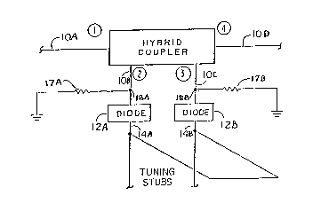
Referring to FIG. 3, there is shown an exemplary
lS e~bodiment of the inv~ntion. Tuning stub~ 14A and 14B are
connected to output terminals 16 (FIG. 2) of diodes 12A and
~28, respectively. Resistors 17A and 1~ are connected
between low points 18A and l~B, respectively, of transmission
lines lOB and lOC, as noted above, the value of eaGh of these
re~lstors is chosen so that the power losses in the
lmpedanGes presented by the ~ranches connected to side ports
2 ~nd a are substantially equal when diodes 12A and 12B are
ln th~ nonconducting state.
The principles of the invention are applica~le to
other bits in the phase ~hifter producing different
ma~nitudes of phase shift. Although the magnitudes of the
impedances are not reciprocally related in OD and off state~
.
-, ' ` : ' ~, ..
~6~)0~
for the lower phase shif~ values, there is a magnitude
di~ferenoe in ef~ectively terminating side ports so at the
low point of the standing wave for one ~tate, there exists a
minimum in the standing wave ratio where a resistor may be
added to provide minimum unhalance between the on and of f
~tates and thereby significantly reduee amplitude modulation.
Other embodiments are within the followin~ claims~
':