Note: Descriptions are shown in the official language in which they were submitted.
12~3639~
-- 1 --
~ DIGITAL FILTER FOR ENHANCEME~T OF DOCUMENT IMAGES
sackground of the Invention
The present invention relates generally to a
method and apparatus for processing digital images,
and in particular, to a method and apparatus for
enhancing digital images from documents containing
background scenes or other spurious images which tend
to obscure or confuse the proper discernment of the
desired images.
In document processing systems, it is ` ;
desirable to enhance certain information on the docu-
ment images which generally consists of hand- or
machine-printed characters. As characters are made of
thin lines, a filter which enhances these lines over
background scenes or other spurious images, improves
the quality of the document images and assists in
di~cerning the content of the images for proper stor-
ing and processing by computer.
U.S. Patent No. 3,973,239 issued August 3,
1976 to Rakumoto et al discloses a pattern processing
system wherein portions of an image detected by a
pickup tube is stored in a matrix. A brute force type
of multiplication is performed wherein a separate
multiplier is used to multiply each element of the
data containing matrix by a ~ingle element of a filter
matrix, and the results summed by an adder. Thus an
m x n matrix requires m x n multipliers. Also, the
apparatus disclosed therein contains shift registers
which shlft downwardly in sequence until the value
being shifted downwardly reaches the bottom of the
data window, and thereafter the value is moved to the
top of the immediately right ¢olumn. This procedure
is foIlowed for all of the columns until the data
matrix is filled.
U.S. Patent No. 3,889,234 issued June 10,
1975 to Makihara et al discloses a feature extractor
:~ ~
,. ,
. - : , , - ,. ,.:
. . - . .
.
. . . .
12~36394
-- 2 --
in which a series of bits representing an image is
simultaneously shifted in a right shift register. In
the disclosed device, all of the data is first set up
in registers and then addressed.
Other examples of character enhancement and
pattern discerning apparatus are disclosed in the
following: U.S. Patent No. 3,737,855 issued June 5,
1973 to Cutaia; U.S. Patent No. 3,805,239 issued April
16, 1974 to Watanabe; u.S. Patent No. 4,047,152 issued
September 6, 1977 to Giuliano et al; u.S. Patent No.
4,052,699 issued October 4, 1977 to Micka et al; U.S.
Patent No. 4,162,481 issued July 24, 1979 to DuValI;
and U.S. Patent No. 4,266,249 issued May 5, 1981 to
Chai et al.
Many sensorg used with optical detection
systems severely attenuate higher frequencies.
Hence, most of the image energy at higher freguencies
i8 due to noise introduced by the imaging system.
When documents are scanned vertically, low frequency
noise ~n the vertical direction appears as very high
frequency noise in the horizontal direction. It is
therefore desirable that higher frequencies, especial-
ly in the horizontal direction, be attenuated by a
filter. This filter should also be capable of enhanc-
ing lines that are approximately two pixels thick.It has been found that black and white line pairs of
two pixels thick are one dimensional spatial square
waves with the fundamental frequency equal to F8/4
where F8 is the sampling frequency of the image.
Hence, the filter should amplify frequencies approxi-
mately equal to F8/4. It has also been found that the
highest frequencies in the image sensed by scanning in
a vertical direction correspond to FS/2. Hence, sinu-
soids with the approximate frequency of FS/2 should
also be attenuated.
: . ' ' . .-
. .. ~ .
; '.' : . ~ ' ~
- ' : . .
~` 1286394
-- 3 --
summary of the Invention
The present invention provides a digital
filter circuit for use with an optical scanning system
which moves a window over the image on a document
being scanned wherein the window is moved one row
downwardly with each picture element that is sensed
from the document. A filter circuit is also provided
which, because of its simplicity, provides for easy
hardware implementation. Also, the coefficients of
the numerical filter are powers of two, providing that
all multiplication operations are achieved by shift
operations. The numerical filter circuit disclosed
herein provides that sinusoids with the approximate
frequency of F8/4 are amplified about 1.5 and about
1.7 times in the horizontal and vertical directions
respectively. Further, attenuation of sinusoids with
the approximate frequency of FS/2 is about 95% in the
horizontal direction and about 45% in the vertical
direction.
It i8 therefore an object of the present
invention to provide an enhancement circuit which
enhances a two-dimensional array of picture elements
of a document being scanned with a minimum of multi-
plier and adder circuits.
It $s a further object to provide an
enhancement circuit which effects a scan line delay
between the scan lines of a data window.
It is a further object to move the data
window down one row with the sequential reading of a
new picture element value.
It i8 a further object to apply a filter
matrix to the picture element values in the data
window which amplifies sinusoids with the approximate
frequency of Fs/4 in the horizontal and vertical
directions, and attenuate sinusoids with the approxi-
mate frequency of FS/2 in the horizontal and vertical
directions.
' ~ - . ~ ' ' . ' ' . ~ ' '
' ' . ~
.
6394
-- 4 --
It is a further object to effect
multiplication of values of the picture elements of
the data window by elements of the filter matrix by
shifting the data bits of the data window elements.
In one preferred embodiment, an apparatus and
method is provided for scanning a document image in an
m x n matrix. The device includes a sensing array for
sequentially sensing along a scan line, elements along
one dimension of the matrix, registers for sequen-
tially storing sensed elements for a selected number
of scan lines, and a circuit for effecting a scan line
delay between sequential scan lines. Registers are
also provided for effecting an element delay in all of
the stored scanned lines along the other dimension of
the matrix wherein the element delay is responsive to
a sequential sensing of a matrix element. Selected
matrix elements are combined with selected weighting
factors for enhancing the document image being
scanned .
Brief Description of the Drawing~
Fig. 1 is a block diagram illustrating a
document reading system utilizing the present inven-
tion;
Fig. 2 is an illustration of the surface of a
document to be scanned by the system of Fig. 1 showing
the rows and columns of picture elements sensed there-
by;
Fig. 3 is a block diagram of a portion of the
filter circuit of Fig. l;
Fig. 4 i8 a timing diagram of control signals
for the circuit of Fig. 3;
Figs. 5A-5C give a graphic illustration of
the functions of the circuit portion of Fig. 3;
Fig. 6 is a diagrammatic illustration of the
matrix of the picture element values read by the
system of Fig. 1 showing the row and column nomencla-
ture thereofs
:. .- .:. . , - - - :
- :. . . - .
-
Z~S639~
- 5
Fig. 7 is a diagrammatic illu~tration of the
weighting values or coefficients of the numeric filter
of the present invention;
Figs. 8A-8C are a graphical representation of
the calculations performed by the numeric filter of
the present invention;
Fig. 9 is a block diagram of a circuit for
accomplishing the solution graphically represented in
Fig. 8C:
Figs. lOA-lOE, arranged as shown to Fig. 10,
is a partial schematic diagram of the circuit illus-
trated in Fig. 9;
Figs. llA-llF, arranged as shown in Fig. 11,
is a partial schematic diagram of the circuit illus-
trated in Fig. 9;
Figs. 12A-12C, arranged as shown in Fig. 12,
is a partial schematic diagram of the circuit illus-
trated in Pig. 9;
Fig. 13 is a map for the arrangement of the
schematic diagram portions of Figs. 10, 11 and 12; and
Fig. 14 is a block diagram of the averaging
circuit of Pig. 1.
ription of the Preferred Embodiment
Fig. 1 is a block diagram illustrating a
document reading system utilizing the present inven-
tion. The document reading system reads a document
such as a check from a banking institution for storage
and processing in a computer. The document contains
certain legal information including the check number,
th~ amount of the check, the date on which the check
iB written, and the signature of the writer which must
be analyzed and discerned for storage in the computer
memory for proper processing of the check. Many
checks contain background scenes or other spurious
images such as ink spatters, stains, or other marks
which tend to obscure or confuse the proper discern-
.
.:
.
. . ~ . . :
- . .
.
, .
- 1286394
-- 6 --
ment of the mentioned legal information recorded on
the check.
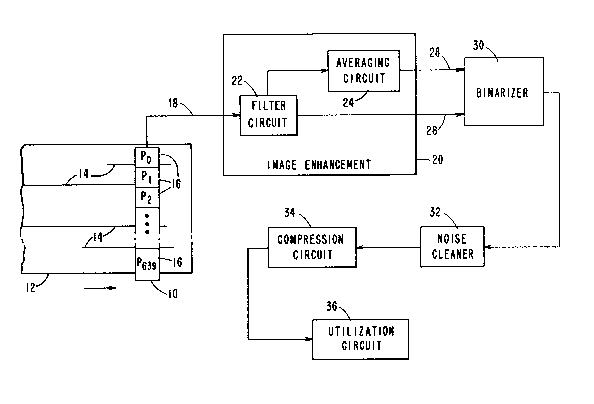
The system of Fig. 1 includes a sensor array
10 which scans in a vertical direction along one
dimension of the check 12. As is known, the sensor
array 10 includes a number of sensors 16 for sensing
the gray levels of small areas of the document
referred to as a picture elements or pixels. In the
preferred embodiment, the sensor array 10 is divided
into 640 sensing elements, numbered from 0 through
639, for reading the pixels of the document. In the
preferred embodiment, the sensing elements 16 are
scanned from top to bottom, and gray values for the
~ensing elements 16 are transmitted, in turn, over a
data bus 18 from the sensing array 10 to the circuits
of the ~ystem to be described. The gray levels of the
preferred embodimént may have one of 64 values ranging
from 0 to 63, with 0 being the darkest and 63 being
the lightest.
The gray levels on the data bus 18 are fed
from the sensor array 10 to an image enhancement
circuit 20 where the gray levels are enhanced in such
a manner that the background scene and other spurious
marks are attenuated. The image enhancement circuit
20 contain6 a filter circuit 22 for performing the
image enhancement function, and an averaging circuit
24 for determining the average gray level of a 3 X 3
pixel window around the pixel being enhanced. The
output of the filter circuit 22 and the output of the
averaging circuit 24 are connected to a binarizer
circuit 30 by data buses 26 and 28 respectively.
- The binarizer circuit 30 converts the 64
values of gray levels of the pixel being enhanced from
6 bits per pixel to a 1 bit per pixel binary signal.
Any of a number of binarizing schemes and circuits may
be employed, as is well known in the art.
.
- . .-
.
. .
. . . . . .
.
:, -. . . . .
~2~63!~
-- 7 --
The binary output of the binarizer circuit 30
is then processed by a conventional noise cleaner
circuit 32, a compression circuit 34, and a utiliza-
tion circuit 36 which may, for example, be banking or
accounting apparatus for storing and processing the
legal information from the document 12.
The digital filter circuit 22 of Fig. 1
applies a 5 X 5 two-dimensional digital filter having
the coefficients:
0 -1 -2 -1 0
-1 1 2 1 -1
1/16 -2 4 16 4 -2
-1 1 2 1 -1
0 -1 2 -1 0
To apply the digital filter described, the.
filter circuit 22 operates on a 5 X 5 matrix of gray
level data from data bus 18 in accordance with the
following equation:
Equation 1:
~1 ~2
R(i,j) z ~ ~W(k,l)D(i+k,j~l)
k =dl i z ~2
where R = enhanced document image elements,
W = weighting values,
D = original document image elements, and
1~ ~ 2~ and ~ 2 are defined.
In the present embodiment wherein a 5 X 5
matrix is operated on by the digital filter, the
matrix dimensions vary from 0 to 4, and the element
being enhanced is the center element R(2,2) of the
matrix. In thi6 case, the values of G~l and ~ 2 are
0, and the values Of ~ 1 and ~ 2 are 4.
, , ,
':'. ' ' . - , , :, ' , . . '
.
: : ~
, . , . .' .' ~ :
..
;394
-- 8 --
Turning to Fig. 2, a document to be scanned
12 is shown including the pixels viewed by the sensor
array 10. The pixels of document 12 will be scanned
in a series of vertical scans in the Y direction from
0 to 639. With each vertical scan, the document 12
will be advanced in the X direction starting with
vertical scan 0 and continuing for the length of the
document 12. The filter circuit 22 of Fig. 1 utilizes
the vertical scans and the separate sensing of each
pixel to establish a window for applying the described
filter. In Fig. 2, each pixel is identified by the
letter P followed by two numbers wherein the first
number identifies the pixel number and the second
number identifies the vertical scan. For instance,
P3,2 identifies pixel number 3 in vertical scan 2.
As the filter utilized by circuit 22 of Fig.
1 is a 5 X 5 two-dimensional matrix, the window upon
which the filter operates i8 not complete until pixel
number 4 of vertical scan 4 has been read. This
window is shown in Fig. 2 and identified as window 1
and extends from vertical scan 0 to vertical scan 4
and from pixel 0 through pixel 4. The columns of
window 1 are alphabetically lettered A through E
starting at the leftmost column (vertical scan 4).
The rows of window 1 extend from pixel number 0
through pixel number 4 and are identified as rows 0
through 4 starting from the lower most row (pixel
number 4) and extending upward. As will be explained,
the pixel being enhanced by window 1 is identified as
P2,2
When the pixel identified as P5,4 is read by
the sensor array 10 of Fig. 1, the window in Fig. 2
will shift downward one row as identified by window 2
in Fig. 2. It will be noticed that in window 2, row 0
extends through pixel number 5 for vertical scans
numbered 0 through 4. Those pixels in row 0 of window
1 now become row 1 of window 2, and pixels in row 1 of
window 1 become row 2 in window 2, etc.
- : -
,
-
12~363~4
g
In this manner, the window operated on by
filter circuit 22 of Fig. 1 is moved downwardly one
row for each pixel read until all 640 pixels of the
sensor array 10 have been read. The next vertical
scan, identified as vertical scan 5, is then started
and the pixels 0 through 639 are sequentially accessed
as before. In this case, the window will return to
the top row of pixels, and the window will move one
column to the left. Thus, column A of the new window
will appear at vertical scan number 5, column B at
vertical scan number 4, etc. The window will then be
moved downwardly as previously described.
It will be understood that the top and bottom
two rows and the right and left two columns of the
document will not contain complete information, and
are processed by conventional border detection tech-
niques as are known.
Fig. 3 is a block diagram of a portion of the
circuit of the filter circuit 22 in which a window for
the 5 X 5 filter as illustrated in Fig. 2 is deter-
mined. The circuit includes random access memories or
RAMs 40 through 43 in which the gray level values of
the pixels illustrated in Fig. 2 are stored. The RAMs
40-43 are in the preferred embodiment, a combination
of RAM chips arranged such that the six bits repre-
sentative of the 64 gray levels from each pixel may be
stored sequentially for all 640 pixel elements in each
~can line. An address circuit 44 is provided which
transmits an address over a bus 46 which is connected
to each of the RAMs 40-43. A signal WE/ is transmit-
ted over conductor 48 to each RAM 40-43 and to address
circuit 44. The signal WE/ causes the address circuit
to increment by 1, and controls the data buses 50-53
of ~he RAMs 40-43 respectively. The contents of the
RAMs 40-43 at the address appearing on the address bus
46 is simultaneously placed on the data buses 50-53
respectively. In this manner, the address circuit 44
.
-
. . . . - '
12~363~
-- 10 --
addresses the RAMs 40-43 from 0-639. When the address
circuit 44 counts through 639, the address circuit
toggles and begins again at address o as will be
explained.
Latches 55-59 are provided to latch the 5
pixel elements of an entire row in the window as
illustrated in Fig. 2. Tri-state devices 60-63 are
provided to control movement of pixel data from the
latches 55-58 into RAMs 40-43 respectively. The data
buses 50-53 of the RAMs 40-43 are connected to the
inputs of the latches 56-59 respectively as shown.
The latches 55-59 are controlled by a signal PXLCLK on
conductor 65. Signal WDATA EN/ on conductor 66 con-
trols the tri-state devices 60-63 allowing data from a
connected latch to be passed through the respective
tri-state device to the data bus of the connected RAM.
As previously described, incrementing of the address
circuit 44 and the writing of data to the RAMs 40-43
is controlled by the WE/ signal. A CS/ signal on
conductor 68 control~ the acceptance of data into RAMs
40-43. A data bus 70 is connected to the data input
of latch 55 as shown, and is a part of data bus 18 for
sequentially reading gray level data signals from the
pixel sensors 16 in the sensor array 10 into latch 55.
Fig. 4 is a timing diagram of the signals
controlling data input from the pixel sensors 16 into
the filter circuit 22. A system clock signal SYSC~K
establishes the timing between the various signals.
The signal PXLCLK which controls the latches 55-59
goes active at 72, thereby causing the pixel data on
data bus 70 to be latched into the latch 55, and data
output from RAMs 40-43 to be latched into latches
; 56-59 respectively. The signal WE/ goes active at 74,
thereby turning o~f the data output of RAMs 40-43.
Next, the WDATA EN/ signal goes active at 76, thereby
activating tri-state devices 60-63 such that the data
latched by latches 55-58 is accepted into RAMs 40-43
:' . - , - .
.
. , .: ' , '
,' .
,' . ' ' . ' -
.
. . .
.
~21363~4
-- 11 --
respectively. Thus, the RAMS 40-43 act as a shift
memory wherein data in RAMs 40, 41 and 42 are shifted
to the right into RAMs 41, 42 and 43 respectively at
the address appearing on address bus 46 of Fig. 3, and
the data from the latest read pixel is read into RAM
40.
The positive-going edge of signal WE/ at 80
causes the address circuit 44 to clock such that the
address is insreased by 1. The address circuit 44
toggles to O when the address reaches 640. The WDATA
EN/ signal goes inactive at 84, thereby disabling tri-
state devices 60-63 such that data in the latches
55-58 is no longer passed to the data buses of the
RAMs 40-43. The CS/ signal then goes active at 86 to
allow data from the RAMs 40-43 to be read into latches
56-59 respectively and data from a new pixel to be
read over data bus 70 into latch 55. The described
sequence then starts over again as described.
As shown in Fig. 3, the output of latch 55
goes to A-bus at 90, the output of latch 56 goes to B-
bus at 92, the output of latch 57 goes to C-bus at 94,
the output of latch 58 goes to D-bus at 96, and the
output of latch 59 goes to E-bus at 98. The signifi-
cance of these buses will be discussed later.
Figs. 5A, 5B and 5C give a graphic
illustration of the functions just described. Fig. 5A
illustrates the reading of pixel P4,4 which completes
the first window shown as window 1 of Fig. 2. As
described, the gray level values of pixel P4,4 is read
into latch 55, and the previou~ly-read gray level
values of pixels P4,3; P4,2; P4,1; and P4,0 are read
into latches 56-59 respectively as shown. The address
which is equal to 4, is applied on address bus 46 to
specify the memory location of RAMs 40-43 from which
the pixel values are to be read. As described in
connection with Fig. 4, when the WDATA EN/ signal goes
active at 76, the pixel values in latches 55-58 are
,
: :
, . ~
.
.:
~Z~i3~
- 12 -
shifted one column to ~he right and read into address
4 of RAMs 40-43 as shown in Fig. 5B. Upon the arrival
of positive-going edge 80 of signal WE/, the address
on address bus 46 is increased to 5, indicating that
the next address to be read from RAMs 40-43 is equal
to 5. Upon the arrival of negative-going edge 86 of
signal CS/, the gray level values of the pixels in
RAMs 40-43 will be made available for reading into the
latches 56-59 respectively. Also, the next-read pixel
will be Ps,4 which is made available to latch 55.
When the signal PXLCLR goes active once again, these
values will be latched into latches 55-59 as previous-
ly explained. It can thus be seen by comparing the
values in the latches 55-59 in Fig. 5A to the values
15 in these latches in Fig. 5C that the window has moved
down one row as graphically illustrated as window 2 in
Fig. 2. Figs. 5A and 5C thus illustrate what can be
thought of as a one scan line delay between each of
the data buse~ A-E. For in~tance, in Fig. 5A all of
20 the pixel~ in the fourth row are located in the latch-
es 55-59. In latch 59, the fourth pixel in scan line
0 of Fig. 2 (column E of window 1) is present, while
in latch 58 the fourth pixel in scan line 1 (column D)
is present. Similarly, a delay of one scan line from
25 scan 1 (column D) to scan 2 ~column C) results in the
fourth pixel of scan line 2 being present in latch 57.
Fig. 6 illustrates a 5 X 5 two-dimensional
matrix of a window such as that shown in Fig. 2,
wherein the pixel elements contained in the matrix are
identified by letter6 and numbers. The letter~ repre-
sent columns and the numbers represent rows in the
matrix. For instance, letter A represents the first
column on the left of the matrix, letter B represents
the next column, letter C the third column, etc. The
number 0 represents the first row starting at the top
of the matrix, the number 1 represents the next row,
the number 2 represents the center row, etc. The
,: :, . .
.. . . .
: , . - '
1286394
-- 13 --
central element C2 is the element being enhanced by
the filter circuit 22 of Fig. 1.
Fig. 7 is a 5 X 5 two-dimensional matrix
containing the numerical values of the weighting
factors of the numerical filter. It will be noted
that the numerical values in Fig. 7 have a North-South
symmetry, and an East-West symmetry. In other words,
the values of the first row North of or above the
central element 16 are equal to the values of the
first row South of or below the central element 16.
Likewise, the values of the second row North of the
central element 16 are equal to the values of the
second row South of the central element 16. Likewise,
the numerical values of the first column West of or to
the left of center element 16 are equal to the numeri-
cal values of the first column East of, or to the left
of, center value 16. Also, the numerical values of
the second column West of center element 16 are equal
to the numerical values of the second column East of
center element 16. These symmetrical properties of
the numeric filter matrix are taken advantage of to
reduce the numbers of multipliers needed to solve
equation 1.
Fig~. 8A, 8B and 8C give a graphical
representation of the solution of equation 1. Fig. 8A
graphically represents the multiplication of each
element of the matrix of Fig. 6 times each element of
the numerical filter matrix illustrated in Fig. 7.
For instance, the product of the element in column B,
row 1 of the matrix of Fig. 6 times the corresponding
element of the matrix of Fig. 7, is (Bo x -1) or -Bo
as shown in Fig. 8A. The remaining elements in the
matrix of Fig. 8A show the results of the correspond-
ing multiplication of the elements of the matrix of
Fig. 6 times the elements of the matrix in Fig. 7.
Fig. 8B is a reorganization of the matrix of
Fig. 8A wherein the common terms have been factored
.
: ~ .. . .
: ~
,
.-
-
1~1!36394
- 14 -
out and the non-zero values of column A have been
moved to be adjacent to the non-zero values of column
E. Fig. 8C is a reorganization of the matrix of Fig.
8B wherein certain adjacent elements of the matrix
have been joined together in blocks. It will be
observed that the absolute value of the elements of
block 100 of row 0 have the same multipliers as the
absolute values of the elements of block 102 of row 1,
block 104 of row 3, and block 106 of row 4. Thus, by
using the window shifting technique of the circuit of
Fig. 3 wherein a window is shifted downwardly one row
for each pixel read into the circuit of Fig. 3, it
can be seen that the absolute values of block 102 can
be found by merely shifting the values determined for
block 100 one row downwardly. Further shifting of the
values downwardly will result in the values of blocks
104 and 106 for rows 3 and 4. The multiplier of
blocks 100 and 106 is -1, and the multiplier of blocks
102 and 104 is +1.
The absolute values of rows 1, 2 and 3 of
block 108 can be found in a similar manner by shifting
the window downwardly with the circuit of Fig. 3.
To complete the calculation of Equation 1,
the products of all the elements of the matrices shown
in Pigs. 6 and 7 are added together to find a grand
total. By making use of the North-South and East-West
symmetry described, Equation 1 for a 5 X 5 two-dimen-
sional window is solved by the use of ten summations
and three multiplications. Since all of the multipli-
ers are powers of 2, these multiplications are accom-
plished by merely shifting bits during the summation
process.
Fig. 9 is a block diagram of a circuit for
accomplishing the solution graphically represented in
Fig. 8C. The solution calculated at each point in the
block diagram of Fig. 9 is abbreviated hereafter by
letters and numbers. A number before a letter indi-
'
.
"~
1286394
- 15 -
cates a multiplication and a subscripted number at the
end of the equation represents the row being operated
on. The letter representæ the column from which the
row element is taken. The column letters and row
numbers correspond to those used in Figs. 8A-8C, as
shown for windows 1 and 2 in Fig. 2. It will be
understood that all elements are summed together.
Thus, the equation (-l)x(Bo+2co+Do) is represented
as -BD2Co. Likewise, the equation (4)x(B2+4c2+D2) is
represented as 4BD4C2.
Fig. 9 is a block diagram representing the
filter circuit 22 of the image enhancement circuit 20
of Fig. 1. Blocks 200, 201, 202 and 203 represent the
vertical scan line delays of the circuit discussed in
connection with Fig. 3, and reference numbers 90'-98'
indicate buses A-E numbered as 90-98 respectively in
Fig. 3. As each pixel sensor 16 as shown in Fig. 1 is
read into filter circuit 22, a new row in the window
of pixels a~ described in connection with Fig. 2 is
read. The pixel elements in this new row are identi-
fied as Ao-Eo at 90'-98' respectively. The leftmost
column of elements 204 of Fig. 9 generally calculates
the values represented by blockc 100, 102, 104 and 106
of Fig. 8C; the central column of elements 206 of Fig.
9 generally calculate~ the central block 110 of Fig.
8C; and the rightmost column of elements 208 in Fig. 9
generally calculate~ the values of block 108 of Fig.
8C.
The values of Bo at 92' and Do at 96' are
~ummed by an adder 210 to give the value of BDo. The
value of Co at 94' i~ multiplied by 2 at 212 and the
product i8 added to the sum determined by adder 210 by
an adder 214. Thus, the output of adder 214 is BD2Co.
AB previou~ly mentioned, the multiplication by 2 of
212 i8 accomplished by shifting the bits of the Co
value at 94' during the summation by adder 214.
.
, , - , - ' , .
.
: . : . . - - -, . .
. . . . . . . . . . .
,; ,. . - , , ~
.. .
: ' . ~- ' ' ' :
., : . - :
` -
- 16 -
The value of BD2Co output by adder 214 is
stored in a latch 216 controlled by the PXLCLK signal
discussed in connection with Figs. 3 and 4. Thus,
latch 216, and similar latches to be discussed in
connection with Fig. 9, effect a one-pixel delay. For
instance, latch 216 latches values of pixels read from
row 0 in the window, wbich are held until the PXLCLK
æignal again goes active, at which time the window as
discussed in connection with Fig. 2 will have moved
one row down. At this time, the row 0 values latched
by latch 216 will become row 1 values in the window.
Thu~, the value of the output of latch 216 represents
BD2C1. The output of latch 216 is input into the
positive side of an adder 218, and the output of adder
214 i~ input into the negative side such that the
output of adder 218 is equal to BD2Cl-BD2Co. Three
pixel delays are effected by latches 220, 222 and 224
connected in series such that the output of latch 224
is equal to BD2C4-BD2C3. The output of adder 218 is
input into the positive side of an adder 226, and the
output of latch 224 is input into the negative side of
adder 226 such that the output of the adder 226 is
equal to BD2Cl-BD2Co+BD2C3-BD2C4. It will be noted
that the output of adder 226 is equal to the sums of
blocks 100, 102, 104 and 106 graphically illustrated
in Fig. 8C. It will further be noted that this por-
tion of the calculation for the enhanced pixel was
accomplished by four adders and four latches.
The value of Co available at bus 94' is
multiplied by 2 at 230 and added to the output of
adder 214 by an adder 232. As previously discussed,
the multiplication function of multiplier 230 is
accomplished by shifting the bits of the value for Co
one position. The output of adder 232 is equal to
BD4Co. The output of adder 232 is delayed two pixels
by latches 234 and 236 as previously described. The
output of latch 236 is multiplied by 4 at 238 to give
.-, , ~ .
~ .
^~` lZ~3~394
- 17 -
the value of 4BD4C2 illustrated in block 110 of Fig.
8C.
The value of Ao at bus 90' and the value of
Eo at bus 98' is summed by an adder 240 and is delayed
one pixel by a latch 242, giving a value equal to AEl.
The output of adder 240 is summed with the output of
latch 242 by an adder 244 and delayed one pixel by a
latch 246 to give a value equal to AEl+AE2. The
output of latch 246 is delayed one pixel by a latch
248, and the output of latch 248 is added to the
output of a latch 246 by an adder 250 to give a value
equal to AEl+2AE2+AE3. This value is equal to the
value represented graphically by block 108 in Fig. 8C.
The output of adder 250 is connected to the
negative side of an adder 252, and the output of latch
236 multiplied by 4 at 238 is input into the positive
side of adder 252 which sums the outputs of columns
206 and 208. An adder 254 adds the outputs of adders
226 and 252 to give a total sum of the values calcu-
lated by columns 204, 206 and 208. The results of the
summation by adder 254 are divided by 16 as represent-
ed by block 256 to give the gray level value for an
enhanced pixel as previously described. The divide-
by-sixteen function of block 254 is actually accom-
plished by shifting the bits in the output of adder
254.
Figs. 10, 11 and 12 joined as shown in Fig.
13 is a schematic diagram of the circuit shown in Fig.
9. This diagram may be understood by those skilled in
the art wherein the manufacturer's number of the
various chips are indicated in the diagram, and the
pin connections of the various chips are identified
around the periphery of each chip. The reference
numerals of the various elements are the same as the
reference numerals of Figs. 3 and 9 with 1000 added
thereto. Thus, the RAM 40 of Fig. 3 is identified on
Fig. lOA as RAM 1040. The outputs of these elements
:,
,
12l 36~394
- 18 -
have the same reference numerals as Figs. 3 and 9 with
2000 added thereto. Thus, the output of adder 240 is
identified as 2240A and 2240B, which has been divided
into conductor groups 2240A and 2240B for clarity.
Like qroups of conductors are iden~ified by the same
reference numbers in Figs. 10, 11 and 12, and will be
readily understood by those skill~d in the art for the
proper interconnection of conductors between Figs. 10,
11 and 12.
In Fig. llF, it will be noted that latch 1260
acts to delay the sign bit 2218C output from adder 218
of Fig. 9 for three pixel delays, and the zero bit
2214Ao from the output of adder 214 of Fig. 9 for two
pixel delays 80 that they may be added in by the
adders 226 and 252 respectively of Fig. 9 to the
correct pixel values.
In Fig. 12C, an overflow-underflow circuit
1262 i8 included to indicate an error in the enhanced
pixel value. The circuit 1262 checks the sign bit of
2254B, and if a negative sign i8 indicated, all of the
output bits on bus 26 of the filter circuit are turned
off to indicate that an underflow error has occurred.
If the seventh bit of the output from adder 1254,
which is found in 2254B, is turned on, all of the
output bits on bus 26 are turned on to indicate that
an overflow error has occurred.
Fig. 14 is a block diagram of the averaging
circuit 24 of Fig. 1. The averaging circuit of Fig. 2
has one input 265 connected to the output of adder 210
shown in Fig. 9, and one input connected to Co at bus
94' of Fig. 9. The averaging circuit of Fig. 12 add6
the products of a 3 X 3 matrix centered on the center
element C2 of the 5 X 5 matrix and divides the sum
total of all of these products by 9 to give an average
value. As previously explained, this averaged value
is used by a conventional binarizer circuit 30 shown
in Fig. 1 to determine a binary value of the enhanced
pixel output of filter circuit 22 as is known.
.. . . . - ~ ~ , .
- . . .
. - . . . .. , : . ~ - :
- . . ~ .- .- .
.. . . .
.
- . .
i21363'3~
- 19 -
Thus, an improved document reading system has
been described which enhances data recorded on the
document by a numerical filter circuit. It will be
understood that the disclosed embodiment described
herein is exemplary only, and that modifications and
changes may be made by those skilled in the art with-
out departing from the spirit and scope of the inven-
tion as set forth in the appended claims.
.. , ., . ~
' . , , , ~ . .' , ~' ~
.
: .. . .
' .' , -
', ~ ' . - ,- . .