Note: Descriptions are shown in the official language in which they were submitted.
1 BACKGROUND OF T~IE INVENTION
2 1. Field of the Invention
3 The invention relates generally to
4 receivers and in particular 9 a remote monitoring
system receiver used with a power distribution network
6 for providing information over the power lines of a
7 network, said receiver having a dual baud rate
8 selector.
9 2. Description of the Prior Art
Remote monitoring systems which are
11 used in conjunction with power distribution networks
12 are well known in the prior art. For example, U.S.
13 Patent Nos. 4,535,447, 4,55û,416 and 4,583,û73
14 describe the various features of remote monitoring
system transmitters. These patents are assigned to
16 the same assignee as this patent and are incorporated
17 herein by reference. Remote monitoring system
18 transmitters are associated with transformers to
19 monitor transformer operation. Each transmitter is
2û connected to the secondary power distribution
21 network. Qt some remote point from the various
22 transmitters, a remote monitoring system receiver is
23 also connected to the secondary power distribution
.
. .
- ' "
:
''~ ,
1 networl<. The transmitters and receivers communicate
2 so that the receiver is provided with a sumrnary oF -the
3 information reflecting the status of each transFormer
4 having a transmitter.
The original system design of a remote
6 monitoring system provided for access by remote
7 equipmen-t originating data links by means of a
8 standard 300 baud telephone channel using
9 off~the-shelf modem interfaces. This is compatible
with most equipment that is available in the utility
11 industry and, in particular, is compatible with
12 portable terminals which are part of the utility
13 operational plan for remote monitoring systems.
14 The proliferation of computing equipment,
particularly, the availability of personal computers
16 with auto dialers, has created a need For more
17 flexible interfaces with the RMS systems. One feature
18 that is in demand is the ability to run at a higher
19 baud rate without sacrificing the capability oF -the
300 baud rate operation. Operation at a higher baud
21 rate is an attractive Feature but the 300 baud rate
22 interface must be maintained. The functional
23 requirement, therefore, is to have one or rnore ports
24 of the RMS receiver operating automatically at either
a 300 baud ra-te or a 1200 baud rate with the rate
;'' '. . '. ~ ' ~ ~ -
: - - : . , ~ , ~ .
.
:
1 determined by the remote equipment originating
2 the data link.
3 There are equipments available today that have
4 the capability of responding to multiple baud rates
automatically. However, these equipments generally
6 use a software subroutine to identify the baud rate of
7 the incoming data and iteratively adjust the
8 responding baud rate to match. In contrast, the
9 invention meets the requirement of providing both a
Eixed low rate (300 baud) and a fixed high rate (such
11 as 1200 baud) operation automatically a-t each data
12 access point.
13 SUMMARY OF THE INVENTION
14 The apparatus according to the invention
comprises a remote monitoring system receiver. The
16 receiver includes a processor having an input/output
17 for receiving and transmittin~ data. The receiver
18 also includes a clock for generating a clock signal
19 and a baud rate generator receiving the clock signal
and generating a high baud rate clock signal and a low
21 baud rate clock signal. Modem means selectively
22 receives/transmits data at the high baud rate and at
23 the low baud rate. The modem means has an indicator
.
, ~ . . . .
:. ,:
.'
24 means for detecting receipt of a high baud rate signal
and for prov:iding a high indicator signal in response
26 there-to. The indicator means also de-tects a low baud
27 rate signal and provides a low indicator signal in
28 response thereto. A switch means has a first input
29 port receiving the high baud rate clock signal, a
second input port receiving the low baud rate clock
31 signal, a control input receiving the high indicator
32 signal and the low indicator signal, and an output
33 port. The output port of the switch means provides
34 the high baud rate clock signal in response to receipt
by the control input of the high indicator signal.
36 The output port of the switch means provides
.... _ _ . _ _ .
--5--
- . . . . .
: ' :, . ,'- . ''''.: . . .- ' .. :
- ' . .
,
:
' '
1 baud rate clock signal in response to receipt by the
2 control input o-f the low indicator signal. The
3 appara-tus also includes a storage register for
4 receiving, storing and -transmitting data be-tween the
processor and the modem in response to the baud rate
6 signal provided by the output port of the switch
7 means. The storage register means has a first data
8 port connected to the input/output of the processor, a
9 second data port connected to -the modem means and a
clock port connected to the output port of the switch
11 means.
12 For a better understanding of the invention
13 its operating advantages and specific objects
14 attained by its use, reference should be had to the
accompanying drawings and descriptive mat-ter in which
16 there is illus-trated and described a preferred
17 embodiment of the invention.
18 BRIEF DESCRIPTION OF THE DRAWINGS
, .
19 In the drawings:
Figure 1 is a block diagram of a remote
21 monitoring sys-tem receiver in combination with other
22 apparatus for providing dual baud rate operation
23 according to the inven-tion.
' .' ' :
' - ' ' - " ' ' ''
' - ' ' ~ : ' ' ' -. ~
.' ~ ' ' ,
~364~
1 Figure 2 is a detailed block diagram
2 illustrating the functional operation oF the invention
3 as shown in Figure 1.
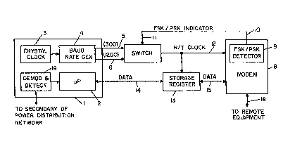
4 ~s shown in Figure 19 remote monitoring
system (RMS) receiver 1 includes a microprocessor 2, a
6 crystal clock 3, a programmable baud rate generator 4
7 and a demodulator and detector 19 connected to a
8 secondary 71 of a power distribution network.
9 Receiver 1 communicates over the secondary 71 to RMS
transmitters 72 which are also associated with the
11 secondary 71. Such RMS transmitters are described in
12 the above-cited patents and are associated with
13 transformers 73 monitor transforrner operation (see
14 Figure 2). The output from the crystal clock 3 is
provided to the baud rate genera-tor 4 so that a
16 generator can be programmed to provide various baud
17 rates. Generally, the invention contemplates any
18 number of baud rates or specific rates may be
19 provided. For simplicity and convenience in
describing the invention, it is assumed that a high
21 baud rate such as 1200 baud and a low baud rate such
22 as 3ûO baud are desired for the preferred embodiment.
23 In general, the operating baud rate o~ the
24 RMS receiver 1 is controlled by the programmable baud
rate generator 4 operating in conjunction with an
. ` : , . . `, . ~' " ~:
. : : - . :
:
'
1 inter~ace. However, the operating baud rate must
2 match the rate oF the remote equipment originating the
3 data link. The in-terface operates in conjunction with
4 a standard off-the-shel-f modem. The standard -for
modems operating at 300 baud is -to use frequency shif-t
6 key (FSK) as the modulation technique. For 1200 baud
7 and higher, phase shift key (PSK) modula-tion is
8 employed. Current off-the-shelf modems which handle
9 multiple baud rates, particularly the smart modem
lû variety, contain internal circuitry to detect whe-ther
11 FSK or PSK data is being received and energize an
12 indicator, such as a light, when the PSK mode is
13 detected thereby indicating a high speed baud ra-te.
14 Such modems then use a software subroutine to identify
the particular baud rate of the incoming data and
16 iteratively adjust the responding baud rate to match.
17 The FSK/PSK indicator is generally
18 available as a control lead on most off-the-shelf
19 modems. The invention relates to the sensing of this
indicator and switching between the various outputs of
21 the baud rate generator 4 to output either the 300
22 baud clock or one of any higher baud rates with a
23 minimum of circuitry. The invention provides this
24 without the need for interaction on the part of a
system operator or the need for specific software
~': ' -, . . '
. . . : , - .
., .
, ' : '.: . :
- ~
~36~
1 within the RMS recelver 1 to evaluate the incoming
2 baud rate. No software subroutine to set a variable
3 baud rate generator is required and -the operator is
~ not required to send a series of test characters -to
allow the software rou-tine to iterate and set the
6 correct baud rate clock.
7 In particular, baud rate genera-tor 4 may
8 be programmed to provide both a 30û baud rate via line
9 5 and a 1200 baud ra-te via line 6. Both these baud
rates are provided to a single pole, double throw
11 switch such as switch 7. Alternatively, switch 7 may
12 be a logic switch or any other switch which would
13 selectively switch between twû or more incoming baud
14 rate signals.
Modem 8 is a standard modem which is
16 linked to remote equipment via telephone line 9.
17 Included within modem 8 is a FSK/PSK detector 9 which
18 evaluates data links originating from the remote
19 equipment. Upon determining the format of the
incoming signal, detector 9 provides an indicator
21 signal via line 10 which indicates whether the
22 incoming signal has an FSK format or a PSK format.
23 This indicator signal is generally a voltage signal
24 such as a ~12 volt signal indicating PSK and a -12
volt signal indica-ting FSK. Line 10 is connected to
_g_
,. ' ' . - :
' ' . ' ~ " ~ ' ~
' ~ ' ' ' ' '
:., . : .
.
~3~ .3
1 the control inpu~ 11 of switch 7 such -that switch 7
2 provides at its output 12 the baud ra-te correspondlng
3 to the indicator provided by detector 9. In
4 particular, i~ de-tector 9 detects an FSK signal and
provides an FSK indicator such as -12 volts via line
6 10, switch 7 is -then switched so -that the incoming 300
7 baud rate via line 5 is provided to output 12.
8 Alternatively, if detector 9 detects a PSK signal
9 originating from the remote equipment and provided by
telephone data link 18, then the PSK indicator is
11 provided via line lû such as a -~12 volt signal
12 resulting in switch 7 connecting input 6 to output 12
13 so that the 1200 baud rate signal is passed.
14 Output 12 of switch 7 then provides the
selected baud rate signal to modem 8 for
16 synchronization and also to an asynchronous storage
17 device such as register 13. Data from and to
18 microprocessor 2 is provided to shift register 13 via
19 line 14 and data from and to modem 8 is provided to
shift register 13 via line 15. Essentially, storaqe
21 register 13 is clocked by the selected baud rate to
22 interface between the modem and the microprocessor so
23 that data may be asynchronoùsly transmitted.
24 Referring to Figure 2, a more detailed
diagram of the invention is presented with -the same
--10--
.
.. ~ . ''"""
' ~ : ',,
.:
.
1 reference characters being used in both Figures 1 and
2 2 for corresponding s-tructure. The embodiment oF
3 Figure 2 is also an expanded version of -the basic
4 embodiment illustrated ln Figure 1. Figure 2 shows
the use of two separate telephone links for accessing
6 RMS receiver 1. In this arrangement, swi-tch 11 is
7 replaced by logic switches 2û and 21. In addition,
8 regis-ter 13 has been replaced by separate asynchronous
9 communications interface adapters (ACIA) 22 and 23
lû which provide the interface between modems 24 and 25,
11 respectively.
12 For illustrative purposes, channel A has
13 been illustrated as communicating with remote
14 equipment at a 12ûû baud rate and channel B has been
illustrated as communicating with remote equipment at
16 a 3ûû baud rate. Referring to channel A, FSK/PSK
17 detector of modem 24 provides the FSK/PSK indicator
18 via line 31. In the case illustrated wherein channel
19 A is communicating at a 12ûû baud rate, line 31 would
carry a PSK indication. Generally, off-the-shelf
21 modems indicate a PSK signal by providing a ~12 volt
22 signal and indicate an FSK mode by providing a -12
23 volt signal. For channel A, line 31 would carry a 12
24 volt signal which would be applied to the input oF
level shift circuit 32. The input to level shift 32
--11-
,~ . , ' . ,
' ' ' ,
. ' . '
.. . .
641~
1 is essentially the control port 11 of switch 7. Level
2 shi~t circuit 32 is used to shift the indicator signal
3 of the modem from the RS 232 format of ~15 volts to
~ logic levels oF OJ-~5 volts. The output of level shi~t
circuit 32, therefore, shifts the +12 volt signal to a
6 0 volt signal which is provided to the inputs of NOR
7 gate 33 and to one of the inputs of AND gate 34. The
8 other input of AND gate 34 comes from line 5 and
9 sùpplies the 5 volt signal toggled at a 300 baud
rate. This signal is indicated in the drawing as
11 5(300). NOR gate 33, which functions as an inverter,
12 provides a 5 volt signal at its output because both of
13 its input signals are O volts. The output of NOR gate
14 33 is provided as one of the inputs to AND gate 35.
The other input to AND gate 35 comes from line 6 and
16 provides the 5 volt signal toggled at a 1200 baud
17 rate. This signal is indicated in the drawing as
18 5(1200).
19 In the case of channel A, the remote
equipment is functioning at 1200 baud so that AND gate
21 35 passes the 1200 baud signal since both its inputs
22 are high whereas AND gate 34 does not pass the 300
23 baud signal because one of its inputs, i.e. the input
24 from the level shift circuit 32, is û. Finally, NOR
gate 36 functions as a summer and passes the 5 volt
-12-
.
. .
- ~ ' .' . . ' ' : ' ' . ''. .
.
: . , .
: . . . - : , ~
,
:
~ 3
1 signal toggled at 1200 baud received from the output
2 of AND gate 25 because the other input o-f NûR gate 36,
3 which comes from the output of QND ~ate 3~, is ~lways
4 O. This 1200 baud clock signal is provided to ACIA 22
which provides a data and clock interface between
6 modem 24 and RMS receiver 1. ACIA 22, as well as ACIA
7 23, are standard ofF-the-shelf items well known in the
8 prior art.
9 Re~erring now to channel B, this channel
has been illustra-ted as operating with remote
11 equipment at a 300 baud rate. Line 41 carries an FSK
12 indicator of -12 volts which is provided to level
13 shift circuit 42. The output oF circuit 42 provides a
14 corresponding +5 volt signal to the inputs oF NOR gate
43 and one of the inputs of AND gate 44. The other
16 input o-f AND gate 44 is provided by line 5 and is the
17 5 volt signal toggled at a 300 baud rate. Since both
18 of the inputs of NOR gate 43 are high, its inverted
19 output is low or O volts and is provided as one of the
inputs of AND gate 45. The other input to AND gate 45
21 comes from line 6 and is the 5 volt signal toggled at
22 a 1200 baud rate. In this channel B case, AND ga-te 44
23 passes the 300 baud rate signal whereas AND gate 45
24 does not pass the 1200 baud rate signal. NOR gate 46
Functions as a summer and passes the 5 volt signal
.. . . . . . . :::.
- ~
. ' ~.
'
~ ~l3~
1 toqgled at a 300 baud rate. This 300 baud rate signal
2 is provided to ACIA 23.
3 The apparatus illustrated in Figure 2 also
4 may include a channel which can be directly connected
-to a terminal for accessing the RMS receiver 1.
6 Switch 50 may be selectively connected to line 5 or
7 line 6 to provide -the approprlate baud rate for the
8 remote terminal to be connected~ The baud rate signal
9 selected is provided via line 51 to ACIA 52 which is
also connected to line 14 for receiving the da-ta
11 information. ACIA 52 will then form an interface
12 between terminal port 53 and RMS receiver 1.
-14-
'' . , ~.
', ~ '
' . ' .