Note: Descriptions are shown in the official language in which they were submitted.
~ 3
VOL~AGE CONTROLLED OSCILLATOR WIT~ HIG~
SPEED CURRENT SWITCHïNG
BACKGROUND OF T~E INVENTION
1. Field of the Invention
The pre ent invention rela~es to voltage
controlled oscillators ~VCO's), and more particularly to
voltage controlled oscillators incorporating
complementary metal oxide ~ilicon field effect
transistor ~CMOS) circuitry. Voltage controlled
oscillators are widely used in phase-locked loop (PLL)
circuits.
A voltage controlled oQcillator operates to
provide an output ~requency which is linearly related to
a control input voltage. Typically~ this is achieved by
providing a capacitor which iæ charged and discharged at
a rate proportional to the control voltage. A
compara~or is provided to switch between charging and
discharging when the voltage on the capacitor goes above
or below first and second reference voltages,
respectively.
2. Descrip~ion of ~he Prior Art
Voltage controlled oscillators including current
source and current sinks for charging and discharging a
capacitor are ~hown ln V.S. Patent Nos. 3,886,408 to
25 Takahashi, 3,904,988 to Hsiao, 4,263,567 to Astle and
4,321,561 to Payne et al. In both the Payne and Hsiao
patents, current switching is provided by switching
transistors which are located in the output curren~
path. Although generally acceptable, such circuits are
30 limited in that the incluæion of æwitching in the output
~LZ136~6
--2--
current pa~h introduces parasitic resistance and
capacitance, thu8 slowing the swi~ching time. In order
for the VCO to operate properly, it is desirable to have
the current sink or source switched as rapidly as
possible so that a uniform charging rate is achieved for
the capaci~or. It i8 no~ pos~ible to achieve such rapid
switching wi~h prior art circuits which include
switching in the output current path.
~ 73
-3-
SUMMARy OF ~HE INV_NTION
The present invention i8 directed to a voltage
controlled oscillator having a high switching speed.
The voltage controlled oscillator of the invention is
capable of running at 10 M~z or above and is thus
suitable for use in the phase-locked loop of a hard disk
data separator. The circuit includes a reference
capacitor which is charged and discharged by means of
output transistor~ operatin~ as a current source or
current sink. The output transistors are connected to
control transistors in a current mirror configuration by
means of transmission gates which are switched to
control operatlon as a current source or current sink.
FET capacitor6 are connected to the gates of the current
15 mirror transistor~ so that the ou~put transistors can be
rapidly switched. This assurPs a uniform charging and
discharging rate for the capacitor which in turn assures
precise oscillator operation.
~Z~73~
--4--
. BRIEF ~ S
The invention will be described with reference to
the accompanying drawings, wherein:
Figure 1 is a schematic diagram of the voltage
controlled oscillator of the present invention; and
Figures 2A-2G are timing diagrams associated with
the present invention.
~2~3~7~
--5--
DESCRIPTION OF THE PREEERRED EMBODIMENT
The following deæcription is of the best
presently contemplated mode of carrying out the
inven~ion. Thi~ descript~on is made for th~ purpose of
illustrating the general principles of the invention and
is not to be taken in a limiting sense~ The scope of
the invention i8 best determined by re~erence to the
appended claims.
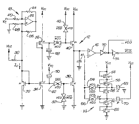
Referring to Figure 1, the present invention is
directed to an oscillator which provides a periodic
output signal VC0 whose frequency is controlled by the
value of an input control voltage Vc. A reference
capacitor 10 is charged and discharged between two
reference voltages under control of charging circuitry
12. The reference voltages are provided by means of a
voltage divider network 14v the output of which is
provided to a compara~or 16 which compareq the reference
voltage to the voltage across the reference capacitor
10 .
The charging and discharging rate of the circuit
is controlled by means of the control input voltage Vc.
This input volta~ge is converted to a control current by
means of a voltage-to-current converter 18. The
voltage-to-current converter includes an input resistor
20, an operational amplifier 22, a feedback resistor 24,
an output resistor 26 and a bias resistor 28. The
operating point of the oscillator is determined by means
of an external resistor 30 which iB chosen to provide a
desired control current level Ic corresponding to a
given input voltage.
The control current Ic supplies and drlves a
reference N-type FET transis~or 32. ~he value of the
reference current flowing through the transistor 32 is
thus dependent on the value of the control input
voltage. The ~ranæistor 32 is connected in a current
mirror configuration to an N-type transistor 34. Due to
the common connection of ~he gates and sources of the
transistors, the current through the transistor 34 will
mirror the current through the transistor 32. The
.. .. . .. . .
7~
--6--
current flowing through the transis~or 34 will also flow
through a P-type transistor 36 whose drain and gate are
connected to the drain o the transistor 34 and whose
source is connected to a power supply Vcc. Thus, a
current will flow through the transistor 34 and 36 and
will have a value which i8 ~e~ermined by the value of
the reference current ~lowing through the transistor 32.
The gates of the transistors 34 and 36 are
coupled to the gates of output transistors 38 and 40,
respectively, via transmission ga~es 42 and 44. The
source of the transistor 38 is connected to ground and
the source of the $ransistor 40 i~ connected to the power
supply, whereas the drains of the transistors are
interconnected and connected to one terminal of the
referewe capacitor 10. The transistor 3~ is thus
coupled to the transistor 34 in a current mirror
configuration, and the transistor 40 is coupled to the
transistor 36 in a current mirror configuration.
The transistors 38 and 40 are alternately
switched on and off to control the charging and
discharging of the reference capacitor 10. In order to
charge the capacitor 10, the transmission gate 44 is
closed to couple the transistor 36 to the transistor 40.
This will turn on the transistor 40 and cause current to
flow through it and charge the reference capacitor 10.
When charging is complete, the transmission gate 44 is
opened and a transmission gate 46 is closed to turn off
the transifitor 40.
In order to ensure precise and rapid switching of
the transistor 40, an FET capacitor 48 is connected to
the gate of the transistor 36. This capaci~or stores a
charge and provides ~ufficient instantaneous current to
quickly switch the transistor 40 to the conductive
state. In the present embodiment of the inventiont the
capacitor 4~ has a value of approximately 30 picofarads
and is biased at 3.5 volts gate-to-source voltage. The
transistor 40 has a size approximately ten times that of
the transis~or 36, and the current through it will be
proportional to the current through the transistor 36
736
--7--
and in direct relation to the relative sizes of the
transistors.
Thus, a current proportional to the control input
voltage will flow ~hrough the transistor 36 and the
transistor 40 will rapidly switch to a conductive state
upon the closing of the transmission gate 44. Current
through the transis~or 40 will thus change in a step
fashion to a level which is propor~ional to the control
input voltage. This current level will determine the
lo charging rate of the capacitor 10.
Whereas ~he transistor 40 operates as a current
source, the transistor 38 operates as a current sink to
discharge the reference capacitor 10. It is rendered
conductive by closing the transmission ga~e 42 to
interconnect the gate of the transistor 38 with that of
the transistor 34. The size of the transistor 38 is
approximately ten times the Rize of the transistor 34,
and the current through it will be proportional to the
current through the transistor 34. Again, an MOS
capacitor 50 is provided so that sufficient
instantaneous curren~ is available ~o rapidly switch the
transistor 38 to ~he conductive state. One terminal of
the capacitor 50 is connected ~o the supply vol~age to
bias the capaci~or 50 to achieve proper MOS capacitor
operation. The value of the capacitor 50 i8 the same as
that of the capacitor 48, i.e., approximately 30 pico-
farads in the present embodiment of the invention. An
additional tran~misslon gate 52 is provided to connect
the gate of the ~ransistor 38 to ground to witch off
the transistor.
High and low reference vol~ages (three volts and
two volts in the presen~ embodiment of ~he invention)
are provided by means of a vol~age divider including
five interconnected transistors 54, 56, 58, 60 and 62.
One of the two reference voltages is provided to the
inverting input of the comparator 16 by appropriately
controlling two transmission gates 64 and 66. The
transmission gates are alterna~ely switched, and MOS
capacitors 68 and 70 are proqided to facilitate rapid
~2~
changing of the value of ~he re~erence voltage applied
to the comparator 16.
The operation of the voltage controlled
oscillator of Figure 1 will be explained with reference
to the timing diagrams of Figure 2~ Initially, the
transmission gate 64 i8 closed and the transmission gate
66 is opened and the reference volta~e applied ~o the
inverting input of the comparator 16 iR thereore three
volts as indicated in Figure 2A. The tran~istor ~0 is
10 turned on and the current through it is a positive value
whose magnitude is determined by the value of the input
control voltage. The capacitor 10 will thus charge up
at a constant rate determined by the magnitude of the
current through the transistor 40, as indicated in
Figure 2D.
When the vol~age on the capacitor 10 reaches
three volts, the output of the comparator 16 will change
states (Figure 2E). Thi~ output i8 applied to a first
inverter 72 to provide the VC0 output. The complement
of this output i~ provided by an inverter 74. These
outputs are provided to the transmission gates 42, 44,
46, 52, 64 and 66.~ The switching of the output causes
the transmission gate 4~ to open and the ~ransmission
gate 46 to close, thereby switching off the transistor
40. Simultaneou~ly, the transmi~sion gate 42 will close
and transmission gate 52 open to render the transistor
38 conductive. The capacitor 10 thus begins dîscharging
through the transi~tor 38~ In addition, the
transmission gate 66 is closed and the trans~is~ion gate
64 opened to change the reference voltage applied to the
comparator from the three volt level to the two volt
level as indicated in Figure 2~. The step change ln the
current through the transis~or 38 as indicated in Figure
2C causes the capacitor to discharge at a constant rate
as shown in Figure 2D. This di~charging ~ontinues until
the two volt level is reached, at which the output of
the comparato~ 16 will again change as shown in Figure
2E, thus changing the states of the output signal~ VC0
and VC0 as shown in Figures 2F and 2G.
2~3~j
- 9 -
The provi~ion of ~he capacitors 48 and 50 enables
the step change and current through the transistors 40
and 38 as shown in Fi~ures 2b and 2c to be achieved. In
addition, the capacitors 6~ and 70 enable a step change
5 in the reference voltage between the three volt and two
volt levels to be achieved. As a result, charging and
discharging rates can be very precisely controlled. Accurate
oscillator oFera~ion can be achieved at extremely high
frequencies necessary for various applications such as
10 use in phase-locked loop data separators in disk drives.
The reference capacltors will charge and discharge
between two reference voltages~ with the rate of
charging being precisely controlled due to the rapid
switching of the transistors 38 and 40.