Note: Descriptions are shown in the official language in which they were submitted.
713~)
PHASE l~ODULATOR APPARATUS
FOR GENERATING A BURST PHASE-MODULATED WAVE
BACKGROUND OF THE INVENTION
The.present invention relates to a phase modulator
apparatus, and more particularly to a phase modulator
apparatus for generating a burst phase-modulated wave,
which is used in a burst signal communication system
such as a TDMA (Time Division Multiple Access)
communication system and an MD-TDM (Multi Directional-
Time Division Multiplex) communication system.
A conventional phase modulator apparatus of this
kind includes a carrier generator for generating a
carrier wave, a phase modulator for phase-modulating
the carrier wave with an input information signal, an
amplifier for amplifying the output of this phase
modulator, a power source for supplying a source voltage
to the oscillator,.the phase modulator and the amplifier,
and a switch for turning on and off in a time-division
burst mode the source voltage supplied to said amplifier,
thereby providing a phase-modulated burst wave from the
output of the amplifier.
In such an apparatus, when the source voltage is
turned on or off in a time-division burst mode, the
current supplied.from the power source varies, thereby
giving rise to fluctuations in voltage drop due to
lZ~7130
-- 2 --
minute resistances present on the power supply line. As a
result, the carrier frequency o~ the oscillator is varied
to adversely affect the modulating performance.
SUMMARY OF THE INVENTION
An object of the invention, therefore, is to provide a
phase modulator apparatus capable of eliminating frequency
variations of the oscillator, caused by fluctuations in
power source voltage during burst mode operation.
A phase modulator apparatus for generating a burst
phase-modulated wave according to the invention comprises
a carrier generator for generating a carrier wave, a phase
modulator for phase-modulating the carrier wave with an
input information signal, an amplifier for amplifying the
output of the phase modulator, a power source for commonly
supp~ying a source voltage to the carrier generator, the
phase modulator and the amplifier, a first switch
responsive to a burst control signal for controlling the
supply of the source voltage to the amplifier, a load
coupled to the power source, and a second switch, connected
to the load in series, responsive to the burst control
signal for operating in a manner mutually complementary
to the first switch.
BRIEF DESCRIPTION OF THE DRAWINGS
FIG. 1 is a block diagram illustrating the structure
of a phase modulator apparatus embodying the present
invention;
lZ87~30
-- 3
FIGS. 2A to 2D constitute a time chart for explaining
the operation of the phase modulator apparatus of FIG. l;
FIG . 3 illustrates a specific example of circuitry
for the switches in the embodiment of FIG. l; and
FIG. 4 is a block diagram illustrating an example of
transmitter-receiver using the phase modulator apparatus
according to the invention.
DESCRIPTION OF THE PREFERRED EMBODIMENT
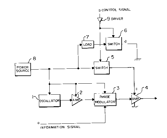
In FIG. 1 showing a phase modulator apparatus of the
present invention, reference numeral 1 represents a carrier
generator for generating a carrier wave; 2 and 4,
amplifiers; 3, a phase modulator; 5 and 6, switches;
7, a dummy load; 8, a common power source and 9, a driver.
Now, the operation of this phase modulator apparatus
will be described by referring to Figs. 2A to 2D showing
waveforms at various points in the apparatus of Fig. 1.
The carrier wave from the generator 1 is amplified
by the amplitude 2 and supplied to the phase modulator 3,
which phase-modulates the amplified carrier wave with
an information signal, i.e., a digitized speech signal a
shown in Fig. 2A. The phase-modulated carrier wave is
amplified by the amplifier 4, which is selectively
actuated by the switch 5. The switch 5 selectively
supplies a current c (Fig. 2C) from the power source 8
to the amplifier 4 in response to a burst control signal b
(Fig. 2B) polarity-inverted by the driver 9.
,~,
-~ , .
.
1287~30
- 4 -
The burst control signal b has, as shown in Fig. 2B,
a time slot Tl, which is allocated for one station and
also repeated every one frame. The frame includes other
time slots (not shown) for other stations.
Thus, the apparatus of each station, i.e., the
amplifier 4 provides an appropriate burst phase-modulated
carrier wave.
The switch 6 featuring the present invention is
connected in parallel to the switch 5 and operates in a
manner complementary to the switch 5. This is, upon
turning on and off the switch 5, the switch 6 is turned
off and on, respectively. When the switch 6 is turned
on, the current d shown in Fig. 2D flows through the
load 7 and the switch 6. If the resistance of the load 7
is adjusted so that the current d flowing through the
switch 6 becomes equal to the current c flowing through
the switch 5, the output voltage of the power source 8
does not vary despite the turning-on/off of the switch 5.
Therefore, the oscillation frequency of the carrier
generator 1 remains unaffected.
The load 7 may be provided between the output of the
switch 6 and the ground.
A specific example of circuitry for the switches 5
and 6 is shown in Fig. 3. According to this example,
the switch 5 consists of a PNP type transistor Trl, a
resistor Rl connected between the base and the emitter,
and a resistor R3 connected between the base terminal
.
'''''
lZ87130
and the switch input. The switch 6 consists of an NPN type
transistor Tr2 and a resistor R2 connected between the base
and the switch input. The collector of the transistor Tr
is connected to the ampli~ier 4 (Fig. 1) and its emitter
is connected to the power source 8 (Fig. 1). The collector
of the transistor Tr2 is connected-to the power source ~
through a resistor RL, as the load 7, and its emitter is
grounded. These transistors implement the complementary
ON/OFF-operations in response to the drive control signal
which is the output of the driver 9.
FIG. 4 is a block diagram showing an example of
transmitter-receiver for use in a TDMA satellite
communication system, to which is applied the present
invention.
As illustrated, this transmitter-receiver consists
of an indoor unit 100 and an outdoor unit 200. A phase
modulator apparatus 10 according to the invention, used
in the indoor unit 100, includes a phase shift-keyed (PSK)
phase modulator for instance, and supplies such a burst
phase-modulated signal as what was referred to above in
response to an information signal a from a baseband
circut 11 and a burst control signal b from a control
signal generator 14. This burst phase-modulated signal
is mixed by a mixer 16 with an output from a synthesizer
17, filtered by a filter 19, amplified by an intermediate
frequency (IF) amplifier 21,and supplied to a multiplexer
24 of the outdoor unit 200 by way of a multiplexer 22
i~'7~30
- 6 -
and a single cable line 23.
In the outdoor unit 200, the output signal from a
multiplexer 24 is converted in frequency into the radio
frequency (RF) band by a local oscillator 26 and an up
converter 27 and, after being amplified by a power
amplifier 29, transmitted by way of a duplexer 30 and
an antenna 31 to a satellite. Meanwhile, a signal from
the satellite is received by the antenna 31 of the outdoor
unit 200 and, after.going through the duplexer 30 and a
low noise (LN) amplifier 28, is converted in frequency
by the local oscillator 26 and a down converter 25. The
converted signal is entered into the multiplexe~ 22 of
the indoor unit 100 via the multiplexer 24 and the cable
line 23. The output from the multiplexer 22, a~ter going
through an IF amplifier 20 and a filter 18, is mixed by
a mixer 15 with an output from the synthesizer 17 and,
after being demodulated by a PSK demodulator 12, is
supplied to the baseband circuit 11. Herein, a controller
13 controls the frequencies of the synthesizer 17.
In summary, according to the present invention, there
is provided, in addition to a first switch for selectively
actuating the amplifier connected to the output of the
phase modulator, a second switch for operating in a
relationship complementary to the first switch to supply
a current to a dummy load which is connected in series to
this second switch. The resistance of the dummy load
is selected so that the currents flowing through the first
1287~30
-- 7 --
and second switches become equal to each other. As a
result, the current flowing from the po~er source is kept
constant to make it possible to eliminate the frequency
variations of the carrier generator attributable to
source voltage fluctuations during burst mode operation.