Note: Descriptions are shown in the official language in which they were submitted.
lZ87131
27598-45
BACKGROUND OF THE INVENTION
The present invention relates to a dielectric filter
comprised of ceramic material, and more particularly to a
dielectric filter and its method of manufacture, to which radio
frequency signals (hereinafter referred to as RF signals) having a
frequency from the ultra high frequency (UHF) bands to the
relatively low frequency microwave bands can be coupled, and which
is well adapted for a bandpass filter coupling to RF signals
having either of the frequency ranges from 825 MHz to 845 MHz or
from 870 MHz to 890 MHz, which are used by mobile telephones.
A dielectric filter must be tuned after the filter is
initially constructed and tested. A conventional dielectric
filter structure whose frequency response may be finely adjusted
is described in detail in U.S. Patent No. 4,431,977 and Japanese
laid-open Patent Publication No. 84-128801, laid-open on July 25,
1984. A fine frequency adjustment of the filter described in U.S.
Patent No. 4,431,977 is performed by removing an amount of the
conductive material from around the conductor-lined holes formed
in the dielectric material, the amount of the material removed
determining the amount of adjustment.
There has been a continuiny effort, particularly in the
field of mobile telephones, to reduce the size of the filters. A
problem arises, however, in reducing the size
'~''
'
'~
lZ87131
of a filter which is tunable in the manner of the prior art
because the amount of conductive material to be removed for
a given adjustment will be necessarily decreased, and thus
the removal process is more sensitive and therefore more
time consuming and expensive.
Another adjustment approach which is described in
Japanese laid-open Patent Publication No. 84-128801 is to
perform the fine frequency response adjustment OI the rilter
by cutting conductive strip lines which are provided on the
top surface, surrounding the holes. This other adjustment
approach may be used to finely adjust the frequency response
of the filter. However, it has been found that with this
approach, portions of the ceramic material provided between
the holes and the strip lines reduce the unloaded Qu of the
filter.
SUMMARY OF THE INVENTION
Accordingly, it is an object of the present invention
to provide an improved dielectric filter whose frequency
response can be finely adjusted without reduction of the
unloaded Qu of the filter.
It is another object of the present invention to
provide an improved dielectric filter which can be easily
tuned and is well adapted for automatic tuning.
lZ87~31
The dielectic filter of the present invention includes
a block of ceramic material having one or more holes
extending from a top surface to a bottom sur~ace, each of
which is interiorly covered with conductive material so as
to form an inner conductive layer. The bottom surfacs and
side surfaces of the block are similarly covered with bottom
and side conductive layers electrically connected to the
inner conductive layers at the bottom surface. The inner
conductive layer is further connected to spaced apart top
conductive layer portions provided on the top surface of
the block surrounding each hole. The top layer portions
are spaced from each other and have an oblique edge portion
which is capacitively coupled with, and obliquely faces an
upper edge portion of the side conductive layers.
As with the known methods of manufacture of dielectric
filters (such as are disclosed in U.S. Patent No. 4,431,977
and Japanese laid-open Patent Publication No. 84-128801),
the filter is designed to initially have a resonant frequen-
cy which is greater than that ultimately desired, and after
measuring the resonant frequency initially obtained, a
portion of the top conductive layer is removed in order to
reduce the resonant frequency to a desired value.
However, the amount by which the resonant frequency
is reduced by removing a portion of the top conductive
- 4 -
1'~87~3~
27598-45
layer depends not only on the amount of material removed, but also
on the distance from the removed portion to the opposing upper
edge portion of the side layer. Therefore, the resonant frequency
of the filter can be, and in accordance with the method of the
invention is, reduced by a predetermined amount by selection of a
location along the oblique edge portion appropriate to the amount
of reduction required for removal of a predetermined amount of
conductive material.
In accordance with another aspect of the invention, the
oblique edge portion of the top conductive layer is straight or
uniformly staircase-shaped and the upper edge portion of the side
layer is straight, so that the distance between them changes in a
linear or uniformly incremental manner. This facilitates the
selection of the appropriate location for the removal of
conductive material depending on the amount by which the resonant
frequency must be reduced.
Each portion of the block of ceramic having such a hole
surrounded by a top conductive layer portion, and having an
interior conductive layer and bottom and side conductive layers,
defines a dielectric resonator whose resonant frequency is reduced
by removing a portion of the top conductive layer portion.
Thus, in accordance with a broad aspect of the
invention, there is provided a dielectric filter, comprising:
a dielectric block having a top surface, a bottom surface and
a side surface extending from the top surface to the bottom
surface, the dielectric block further having an interior surface
defining a hole extending from the top surface to the bottom
S,.~
'
-,
. . ,
12~'713~ 27598-45
surface;
a side conductive layer covering the side surface;
a bottom conductive layer covering the bottom surface and
electrically connected to the side layer, the side layer having an
upper edge portion adjacent to the top surface;
a top conductive layer on a portion of the top surface
surrounding the hole;
an inner conductive layer covering the interior surface so as
to be electrically connected to the bottom layer at the bottom
surface and the top conductive layer at the top surface, the top
conductive layer being spaced from the side layer and having a
side edge portion obliquely opposing and being capacitively
coupled with the upper edge portion.
In accordance with another broad aspect of the invention
there is provided a dielectric filter, comprising:
a dielectric block having a top surface, a bottom surface and
two opposite first side surfaces, the dielectric block further
having a plurality of interior surfaces defining respective holes,
the holes extending from the top surface to the bottom surface and
0 being arranged between the two first side surfaces;
side conductive layers covering the two first side surfaces
and a bottom conductive layer covering the bottom surface and
electrically connecting the side layers, the side layers having an
upper edge portion adjacent to the top surface;
a plurality of top conductive layers on respective portions
of the top surface surrounding the respective holes;
inner conductive layers respectively covering the interior
- 5a -
lZ87131
27598-45
surfaces, the inner layer of each interior surface electrically
connecting the bottom layer to the top layer surrounding the hole,
each top layer having a side edge portion obliquely opposing the
upper edge portion so as to be capacitively coupled with the upper
edge portion, whereby the frequency response of the filter can be
adjusted by removing a predetermined same amount of at least one
of the top layers from a selected location along the side edge
portion, the location being selected according to the amount of
adjustment desired.
In accordance with another broad aspect of the invention
there is provided a method of manufacturing a dielectric filter of
selected resonant frequency values, the filter including a
dielectric block having a top surface, a bottom surface, and two
of opposite side surfaces, the dielectric block further having
interior surfaces defining a plurality of holes extending from the
top surface to the bottom surface between the side surfaces, the
method comprising the steps of:
(a) covering the side surfaces with a conductive material so
as to produce a side conductive layer having an upper edge portion
adjacent to the top surface;
(b) covering the bottom surface with conductive material so
as to produce a bottom conductive layer electrically connecting
the side conductive layer;
(c) covering respective spaced apart portions of the top
surface surrounding the holes with conductive material so as to
produce respective spaced apart top conductive layer portions
thereon;
- 5b -
lZ~7131
27598-45
(d) covering each of the interior surfaces with conductive
material so as to produce a plurality of inner conductive layers,
each of the inner layers being electrically connected to the
bottom layer and the respective top layer portions, each of the
top layer portions having a side edge portion obliquely facing the
upper edge portion so that the side edge portion is capacitively
coupled with the upper edge portion, so as to produce a dielectric
filter having resonant frequencies greater than the selected
resonant frequency values;
(e) measuring the resonant frequencies of the filter; and
(f) removing a predetermined amount of the conductive
material from respective selected portions of the side edge
portion depending on the measured resonant frequencies, so as to
reduce the resonant frequencies of the filter to the preselected
resonant frequency values.
In accordance with another broad aspect of the invention
there is provided a method of manufacturing a dielectric resonator
of selected resonant frequency value, the resonator including a
dielectric block having a top surface, a bottom surface, and a
side surface, the dielectric block further having an interior
surface defining a hole extending from the top surface to the
bottom surface, the method comprising the steps of:
(a) covering the side surface with a conductive material so
as to produce a side conductive layer having an upper edge portion
adjacent to the top surface;
(b) covering the bottom surface with conductive material so
as to produce a bottom conductive layer electrically connecting
;, '~
~,
~Z~7131
27598-45
the side conductive layer;
(c) covering a portion of the top surface surrounding the
hole with conductive material so as to produce a top conductive
layer portion thereon;
(d) covering the interior surface with conductive material
so as to produce an inner conductive layer, the inner layer being
electrically connected to the bottom layer and the top layer
portion, the top layer portion having a side edge portion
obliquely facing the upper edge portion so that the side edge
portion is capacitively coupled with the upper edge portion, so as
to produce the dielectric resonator having a resonant frequency
greater than the selected resonant frequency value;
(e) measuring the resonant frequency of the resonator; and
(f) removing a predetermined amount of the conductive
material from a selected portion of the side edge portion
; depending on the measured resonant frequency, so as to reduce the
resonant frequency of the resonator to the preselected resonant
; frequency value.
BRIEF DESCRIPTION OF THE DRAWINGS
These and other features and advantages of the invention
will be more completely understood from the following detailed
description of the preferred embodiments with reference to the
accompanying drawings in which:
. .
5d -
~~~
-
~Z8713~
- Fig. 1 is a perspective view of a first embodiment of
a dielectric filter in accordance with the present-inven-
tion;
Fig. 2 is a cross section of the dielectric filter
shown in Fig. 1, taken along lines A-A;
Fig. 3 is a partial plan view from the top of the
dielectric filter in Fig. l;
Fig. 4 is a graph illustrating the relation between
the reduced resonant frequency and the trimming area
according to the selection of the trimming portion from
the edge portion of the top conductive layer in Fig. 3; and
Figs. 5-8 are partial plan views of other embodiments
of the dielectric filter according to the present invention
showing one of four identical holes in the filter and
surrounding conductive layer.
DETAILED DESCRIPTION OF 'r~ PREFERRED EMBODIMENT
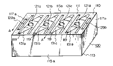
Referring to Fig. 1, there is illustrated a dielectric
filter 100 embodying the present invention.
The filter 100 includes a substantially rectangularly
shaped block 110 of ceramic materials, primarily BaO and
Tio2. The block 110 has a top surface 111, a bottom
surface 113, a pair of mutually parallel first side
surfaces 115a and 115b and a pair of mutually parallel
-- 6 --
12~7131
second side surfaces 117a and 117b. The block 110 further
has four cylindrical interior surfaces 118 therein which
respectively define corresponding holes 119 each extending
from the top surface 111 to the bottom surface 113 and
arranged in a vertical plane parallel to the first side
surfaces 115a and 115b. Each of the interior surfaces in
the block 110 is entirely covered with a layer of a
conductive material such as a silver or copper so as to
form inner conductive layers 121a, 121b, 121c and 121d as-
shown in Fig. 2, which is a cross section of the dielectricfilter 100 in Fig. 1 taken alonq lines A-A.
Referring to Fig. 2, the inner conductive layers
121a-121d are electrically connected with one another by
means of a bottom conductive layer 123 which may also be
e~a~P/6
~5 formed, for oxampi,c of silver or copper on the bottom
surface 113 of the block 110. The bottom conductive layer
123 is electrically connected with similarly formed side
conductive layers 125 provided on the side surfaces 115a,
115b, 117a, and 117b.
Each of the four inner conductive layers, surrounded by
the dielectric material enclosed in the side and bottom
conductive layers, acts as a dielectric resonator which is
1287131
resonant with predetermined RF signals inputted from an
input electrode 129a and outputted to an output electrode
129b.
The four resonators have respective top conductive .
layers 131 on the top surface 111, designated layers or
layer portions 131a, 131b, 131c and 131d. The top conduc-
tive layers 131a-131d respectively form collars covering
the portions of the top surface 111 surrounding the four
corresponding holes 119 and are respectively connected to
the corresponding inner conductive layers 121a-121d.
The thickness of each of the conductive layers 121,
123, 125 and 131 is about 2 microns.
Referring to Fig. 3, there is illustrated a partial
plan view of the filter 100 shown in Fig. 1. The exemplary
top layer 131 as shown in Fig. 3 has a rectangular con-
figuration, and has side edge portions 126a and 126b
respectively facing the straight upper edge portions 125a
and 125b of the side conductive layer 125. The side edge
portions 126a and 126b are respectively provided with
substantial identical right angled triangle shaped recesses
127a and 127b.
According to the first embodiment, the width (a) of
the filter 100 is 6.00mm; the width (b) of each top layer
131 is 3.00mm; each of the distances (cl) and (c2) between
1287131
2759~-45
the side portions 126a, 126b and the upper edge portions 125a,
125b is O.smm; the length (d) of the top layer 131 is 5.00mm; the
depths (el) and (e2) of the recesses 127a and 127b are each
1.50mm; the diameter (f) of the inner conductive layer 121 is
2.00mm; the lengths (gl) and (g2) of the sections of each of the
conductive layer edge portions 126a and 126b which are parallel to
the upper edge portions 125a and 125b is 0.50mm; and the base (h)
of each of recesses 127a and 127b is 2.00mm.
The frequency response of a resonator having the above-
mentioned structure can be adjusted by changing its capacitance
which is mainly established between the upper edge portions 125a
and 125b and the side edge portions 126a and 126b including the
straight oblique edge portions 128a and 128b formed by the
recesses 127a and 127b. The capacitance can be reduced by
removing in the form of a notch 130 a portion of the top
conductive layer 131 by means of a sandblast trimmer or a laser
trimmer.
The amount of reduction in the capacitance is determined
by the location or locations of one or more such notches 130 along
the oblique edge portions 128a and 128b, defined, for example, by
its X-coordinate as measured along the upper edge portions 125a
and 125b as shown in Fig. 3.
lZ87~31
As shown in Fig. 4, in the case of removing conductive
material at the location on the oblique edge portion 128b
defined by the X-coordinate Xl, the resonant frequency of
the resonator is sharply reduced because the oblique edge
portion 128b at X1 is relatively close to the upper edge
portion 125b and, therefore, sets up a relatively large
capacitance with the upper edge portion 125b. On the other
hand, in the case of removing the conductive material from
the oblique edge portion 128b at X3, the resonant frequency
of the resonator is only slightly reduced because the
oblique edge portion at X3 is relatively far from the upper
edge portion 125b and, therefore, creates a relatively
small capacitance with the upper edge portion. In the case
of removing the conductive material from the oblique edge
portion 128b at X2, the resonant frequency of the resonator
experiences an intermediate reduction.
The resonant frequency of the resonator, therefore,
can be adjusted within a large range of values by choosing
a trimming location on an oblique edge portion and forming
there a notch of a dimension previously selected indepen-
dently of the location.
In the first embodiment shown in Fig. 3, the X-coor-
dinates Xl and X2 are respectively distances il and i2 from
the conter location X2 equal to .75mm and distances il and
-- 10 --
1287131
i2 from the respective extremes of the oblique edge portion
128b equal to 0.25mm.
The resonant frequency of the resonator in Fig. 3, of
which the center frequency is around 880MHz, is reduced by
2.0MHz in the case of removing 1.57mm2 of the conductive
material from the oblique edge portion 128b at the X-coor-
dinate Xl and is reduced by 0.2MHz in the case of removing
1.57mm2 of the conductive material from the oblique edge
portion 128b at the X-coordinate X3.
There will now be described four additional embodi-
ments of the invention which differ from the first embodi-
ment only in the shape of each of the top surface conduc-
tive layers surrounding each of the holes 119.
Referring to Fig. 5, there is illustrated a second
embodiment according to the present invention. The
conductive layer 531 in Fig. 5 has a rectangular configura-
tion, of which the length (a) is 5.00mm, the width (b) is
4.0mm, and side edge portions 532a and 532b, facing each of
upper edge portions 525a and 525b, are provided with
respective regular trapezoid shaped recesses 526a and 526b.
Each of the trapezoid shaped recesses has a short side (c)
2.40mm long and a height (d) of l.OOmm, and also has two
staircase-shaped oblique sides, respectively consisting of
four steps, each of the treads of which is 0.20mm long and
-- 11 --
lZ~131
each of the risers of which is 0.25mm high. The other
dimensions of the resonator in Fig. 5 are substantially the
same as those of the resonator shown in Fig. 3. The
staircase-shaped oblique sides facilitate automation of the
trimming process by reducing the need for precision in
locating the X-coordinates where the notch is to be placed.
Referring to Fig. 6, there is illustrated a third
embodiment according to the present invention.
The top conductive layer 631 in Fig. 6 has
staircase-shaped edge portions 632a and 632b respectively
facing upper edge portions 625a and 625b, each of four steps
thereof defining a right-angle triangle-shaped recess. The
tread of each of the steps is l.Omm long and the riser of
each step is 0.4Omm high. The other dimensions of the
resonator shown in Fig. 6 are substantially the same as
those of the resonator shown in Fig. 5. This embodiment
has a similar advantage to that of Fig. 5 in reducing the
need for precision in locating where the notch is to be
placed, particularly in an automated trimming process.
Referring to Figs. 7 and 8, there are illustrated two
other embodiments according to the present invention.
The conductive layer~ 731 in Fig. 7 has a paral-
lelogram configuration, having a pair of edge portions 732a
- 12 -
1287131
and 732b obliquely facing respective side conductive layer
upper edge portions 725a and 725b.
The conductive layer 831 in Fig. 8 has a configuration
in which edge portions 832a and 832b, respectively obliquely
facing conductive side layer upper edge portions 825a and
825b, curve away from the latter edge portions from left to
right and from right to left, respectively.
In each of the top conductive layers surrounding holes
119 according to the above-mentioned embodiments, locations
along obligue edge portions have varying predetermined
distances from the outer conductive layer edge portion.
Thus, the resonant frequency of the resonator can be
reduced from a relatively large amount to a relatively
small amount by removing a predetermined same amount of the
conductive material from an appropriately selected location
along the oblique edge portion. The top surface of the fil-
ter is covered with a regular pattern of the conductive
layers surrounding the holes to form with the upper edge
portions 125a and 125b a plurality of resonators. Since
there are no exposed portions of ceramic material on the top
surface between the inner conductive layer and the top
conductive layer, little reduction of the unloaded Qu of the
filter will occur.
- 13 -
128~131
27598-45
It will be understood that the above description of the
present invention is susceptible to various modifications,
changes, and adaptations, and the same are intended to be
comprehended within the meaning and range of equivalents of the
appended claims.