Note: Descriptions are shown in the official language in which they were submitted.
1;~871~2
01 -- 1 --
02 This invention relates in general to
03 microwave oscillators, and more particularly to a
04 waveguide circuit for stabilizing operation of a field
05 effect transistor mounted in fin line at the center of
06 a microwave oscillator.
07 A current objective in the field of
08 miCroWaYe component design is the realization of
09 completely integrated fin line oscillator circuits.
10 Most microwave component designers have avoided the
11 use of three terminal devices such as field effect
12 transistors (FETs) mounted in fir. line, for the reason
13 that commercially available devices are known to
14 become potentially unstable over a predetermined range
15 of frequencies. It has been found that during normal
16 operation of FET transistors, certain combinations of
17 impedances presented to the gate and drain terminals
18 result in large VSWR (Voltage Standing Wave Ratio)
19 signals being developed thereacross, leading to
20 oscillation of the device.
21 When field effect transistors are mounted
22 in a waveguide structure (ie. in fin line) having a
23 cutoff frequency which is sufficiently high that no
24 propagation occurs in the potentially unstable
25 frequency range, the transistors have been found to
26 oscillate uncontrollably within the unstable frequency
27 range below the waveguide cutoff frequency, as a
28 result of the afore-mentioned large VSWR signals being
29 developed across the gate and drain terminals.
In addition, when three terminal devices
31 such as field effect transistors are mounted in fin
32 line circuits, problems have been found to arise due
33 to poor isolation between the input and output ports
34 of the transistors. This results from the fact that
35 electric and magnetic fields and currents are more
36 distributed about the cross-section of a fin line
37 structure than, for example, around a microstrip
38 line. Thus, in fin line, energy passes around a FET
39 transistor rather than coupling into it.
12~3713Z
01 - 2 -
02 Poor input/output port transistor
03 isolation has been found to give rise to spurious
04 oscillations and diminished amplifying ability within
05 fin line circuits. Thus, when used in a microwave
06 oscillator, the poor isolation characteristics of fin
07 line mounted FET transistors leads to unpredictable
08 frequencies of oscillation and poor output power
09 capability.
One prior art FET microwave oscillator is
11 described in an article by A. Jacob and C. Ansorge
12 entitled STABILIZED FIN LINE FET OSCILLATORS,
13 Proceedings of the 13th EuMC Conference, 1983, pp.
14 303-307. The prior art oscillator utilizes an
X-shaped arrangement of fin-lines with three arms used
16 for tuning while the fourth is used for coupling
17 output power. The three terminal FET transistor is
18 mounted in the center of the device, with the gate
19 terminal connected to the input fin line, the drain
terminal connected to the output fin line, and the
21 source terminal connected to coplanar waveguides.
22 A major drawback of the prior art
23 arrangement is that appreciable coupling has been
24 found to exist between the input and output fin line
slots at the center of the structure, resulting in
26 unpredictable feedback between the gate and
27 drain terminals of the FET transistor, such that
28 extensive empirical tuning is necessary in order to
29 generate the required output frequency signal. This
feedback also prevents predictable design of matching
31 circuits required for maximizing the output power of
32 the oscillator.
33 Another disadvantage of the prior art
34 arrangement is that there is no provision for
stabilizing the FET transistor for operation at below
36 the cutoff frequency of the waveguide.
37 As a result of the above-noted
38 disadvantages, many fin line circuits have been
. ~ .
lZ1~132
01 - 3 -
02 constructed utilizing two-terminal devices such as
03 diode oscillators (Gunn and IMPATT). However, such
04 two-terminal devices have been found to suffer from
05 stability, mounting, and reproducibility problems not
06 normally encountered when using FET transistors.
07 Various other prior art waveguide
08 structures are wel~ known which utilize FET
09 transistors mounted between input and output ports
thereof. However, such waveguide structures typically
11 utilize microstrip circuitry as opposed to mounting
12 the transistors in fin line. Stabilizing bias
13 circuits are typically utilized to maintain FET
14 stability at below the cutoff frequency of the
waveguide. These circuits are designed to load the
16 transistor (ie. provide a low VSWR signal to the
17 transistor) at below the cutoff frequency of the
18 waveguide, so as to appear transparent to the
19 waveguide when operated at above the cutoff frequency.
However, such microstrip waveguide
21 structures have been found to suffer from stability
22 mounting and reproduction problems not found in
23 fin line structures.
24 Additional prior art devices are known in
which FET low noise amplifiers are constructed in
26 microstrip, and connected to the front end of a
27 fin line microwave structure. However, these
28 arrangements necessitate the use of a transition from
29 microstrip to fin line, which results in degradation
in the noise figure performance and an increase in the
31 5i ze of the receiver.
32 According to the present invention, a
33 waveguide structure is provided with isolation between
34 the input and output fin lines, resulting from
physically separating the fin lines with a metallic
36 septum or wall. Separate input and output waveguides
37 which share the common wall or septum are provided for
38 each fin line. A dielectric substrate passes through
~28~132
ol 4
02 the spectum, and a printed metallic strip with plated
o3 through holes is located on each side of the substrate
04 along the length of the septum. The plated through
o5 holes provide an electrical contact for both radio
06 frequency (RF) and direct current (DC) energy from one
07 side of the substrate in contact with the septum, to
08 the other side which is also in contact with the
09 septum. The holes are placed sufficiently close
together that no leakage of energy occurs from one
11 waveguide to the other, thereby ensuring proper
12 isolation between the input and output fin lines.
13 A field effect transistor is attached to
14 the center strip and bond wires are placed from the
source terminal to the center strip, and from gate and
16 drain terminals of the transistor to the input and
17 output fin lines respectively. Thus, the input and
18 output fin lines, and hence the gate and drain
19 terminals of the FET transistor are isolated, thereby
overcoming the prior art disadvantages of
21 unpredictable feedback, spurious oscillation, and low
22 output power.
23 Furthermore, the disadvantages associated
24 with prior art two-terminal devices are overcome by
use of a FET fin line circuit.
26 In general, according to the present
27 invention there is provided a waveguide for
28 stabilizing operation of a three port device mounted
29 in fin line at the center of an oscillator circuit
having a predetermined resonant frequency. The
31 waveguide is comprised of a rectangular waveguide
32 housing characterized by a predetermined cutoff
33 frequency, a planar dielectric substrate extending
34 lengthwise through the housing, and a metallization
layer deposited on the substrate. The metallization
36 layer is patterned forming a center strip extending
37 lengthwise through the housing, and input and output
38 fin lines extend lengthwise through the housing on
39 either side of the center strip. A first terminal of
the transistor is connected to the input fin line, a
lZ8~132
01 _ 5 _
02 second terminal thereof is connected to the output fin
03 line, and a third terminal thereof is connected to the
04 center strip. A metallic septum extends lengthwise
05 through the housing along the center strip and
06 orthogonal to the substrate. The septum physically
07 separates the input and output fin lines, thereby
08 isolating and preventing coupling between the first
09 and second terminals of the three port device for
stabilizing operation thereof at frequencies above and
11 below the predetermined resonant frequency.
12 A better understanding of the present
13 invention will be obtained with reference to the
14 detailed description below in conjunction with the
following drawings in which:
16 FIGURE lA is a partially broken
17 perspective view of a FET fin line oscillator circuit
18 according to the prior art,
19 FIGURE lB is a plan view of a dielectric
substrate supporting input and output fin lines and a
21 FET transistor according to the prior art
22 configuration of FIGURE lA,
23 FIGURE 2A is a plan view of one surface of
24 dielectric substrate supporting input and output fin
lines in accordance with the present invention,
26 FIGURE 2B is a bottom view of an opposite
27 surface of the substrate shown in Figure 2A,
28 FIGURE 2C is a cross-sectional end view of
29 a waveguide embodying the substrate shown in Figures
2A and 2B,
31 FIGURE 3 is a detailed cross-sectional
32 plan view of the waveguide in accordance with a
33 preferred embodiment of the present invention, and
34 FIGURE 4 is a cross-sectional view taken
along the line A-A in Figure 3.
36 Turning to Figures lA and lB, a prior art
37 FET fin line oscillator circuit is illustrated,
38 comprised of an X-shaped dielectric substrate 1 having
39 a metallization layer 3 deposited thereon, and a pair
of tapered slots 5 and 7 defining input and output
41 fins of the waveguide.
12137132
01 - 6 -
02 The input and output fin line slots 5 and
03 7 are tapered exponentially, and are characterized by
04 a length of one wavelength at the oscillator resonant
05 frequency, and are fitted for minimum reflection at
06 the waveguide output.
07 A waveguide housing 9 (Figure lA)
08 surrounds the substrate 1, and a plurality of isolated
09 sliding short circuit blocks llA, llB and llC tFigure
lB) are mounted within the housing along three of the
11 four substrate branches.
12 A FET transistor 13 is attached between
13 the two unilateral fin line slots 5 and 7 at the
14 centre of the circuit board, and the mounting is
symmetrical with respect to the drain-gate axis.
16 Bias voltage is introduced to the gate and
17 drain terminals of the FET 13 by means of external
18 microstrip line connections 15A and 15B (Figure lB).
19 Bias low-pass filters to prevent leakage of the radio
frequency oscillation signal from entering the bias
21 circuits may be included either in the form of
22 microstrip filters on the fin line substrate (not
23 shown) or externally connected to microstrip lines 15A
24 and 15B.
In order to prevent a DC short circuit
26 between the bias lines 15A and 15B and the waveguide
27 hou~ing, the metallization layer 3 must be D.C.
28 isolated from the waveguide housing and the sliding
29 short circuit blocks~
In operation, bias voltage is applied to
31 the gate and drain terminals of FET transistor 13 via
32 microstrip line connections 15A and 15B, and a
33 feedback path (not shown) is established by means of a
34 metallic strip extending along the under surface of
the substrate 1 between the drain and gate terminals.
36 The sliding blocks llB and llC are then carefully
37 adjusted to provide the appropriate low VSWR signal
38 for application to the FET 13. Tuning block llA is
12~7132
01 - 7 -
02 then adjusted in order to establish a predetermined
03 input imped~nce for causing resonant oscillation of
04 the waveguide structure.
05 For frequencies above the cukoff
06 frequency, the structure acts as an amplifier for
07 signals applied to the input fin-line 5. In this
08 configuration shorting block llA is omitted. ~owever,
09 as discussed above, coupling between the two
boomerang-shaped slots 5 and 7 in the center of the
11 device has been found to lead to unpredictable
12 feedback between the FET 13 gate and drain terminals,
13 resulting in spurious oscilIation and degraded output
14 power.
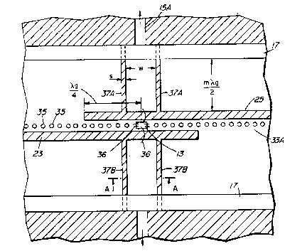
Turning to Figures 2A, 2B and 2C, a
16 waveguide structure is shown according to the present
17 invention comprised of an external housing 17
18 (Figure 2C) surrounding a dielectric substrate 19
19 having a metallizaton layer 21 deposited on a surface
thereof.
21 A pair of exponentially tapered slots 23
22 and 25 in the metallization layer 21 define input and
23 output fin lines respectively, and a metallic septum
24 27 (Figure 2C) extends perpendicular to the substrate
19 on both sides thereof, through the center of the
26 housing 17 for isolating the input and output fin
27 lines. Thus, an input waveguide 29 is established
28 within the housing 17 on one side of the septum, and
29 an output waveguide 31 is established on the other
side.
31 Center metallization strips 33a (Figure
32 2A) and 33b (Figure 2B) extend lengthwise along both
33 surfaces of the substrate 19, and are connected to
34 both halves of the septum 27. A plurality of metallic
plated-through holes 35 extend between the metallic
36 center strips 33a and 33b through the substrate 19,
37 for providing electrical contact between respective
38 halves of the septum. The holes 35 are placed closely
12~132
01 - 8 -
02 together in order to preven-t leakage of energy from
03 the input waveguide 29 to the output waveguide 31, and
04 vice versa.
05 With reference to Figure 3, a field effect
06 transistor 13 is shown attached to the center strip
07 33a with bond wires 35a connected from the source
08 terminal to the center strip 33a, and from the ~ate
09 and drain terminals 36b to the patterned metallization
layer 21 defining the input and output fin lines,
11 respectively. Although not shown, a small groove is
12 preferably cut in the septum 27 in order to house the
13 FET transistor 13.
14 Since the input and output fin line slots
23 and 25 are required to be terminated, a short
16 circuit termination is made one quarter wavelength
17 (ie. ~g/4 with respect to the oscillator resonant
18 frequency) beyond the gate and drain terminal bond
19 wires 36 of the FET transistor 13. This results in an
open circuit in shunt with the gate and drain
21 terminals of the FET transistor 13 at the resonant
22 frequency, thereby ensuring good coupling of radio
23 frequency ~RF) currents into and out of the terminals
24 of FET 13.
In order to bias the FET 13, a pair of
26 microstrip lines 15A and 15B extend through the
27 outside walls of the housing 17, for connection to the
28 gate and drain terminals respectively of FET 13. Two
29 pairs of parallel slots 37A and 37B are made in each
of the input and output fin lines, for isolating the
31 point of contact of the gate and drain terminals of
32 FET 13. The portions of metallic layer 21 surrounded
33 by the slots 37A and 37B and enclosing the gate and
34 drain terminals, function as coplanar waveguides in a
manner similar to the extra two waveguide branches of
36 the prior art arrangement shown in Figures lA and lB.
37 The coplanar bias circuit comprised of
38 slots 37A and 37B is typically connected to the
1~37132
01 -- 9 -
02 source of bias voltage by means of a low-pass circuit
03 (not shown) constructed outside the waveguide housing
04 17, and connected thereto via the microstrip lines 15A
05 and 15B. The low-pass cutoff frequency is preferably
06 selected to provide high signal rejection above the
07 cutoff frequency of the waveguide.
08 Turning briefly to Figure 4, which shows a
09 cross-section of the coplanar waveguide portion taXen
10 along the lines A-A in Figure 3, the pair of parallel
]1 slots 37B are shown separated by a distance W, each
12 slot having a width designated as S. The impedance of
13 the coplanar waveguide structure can be altered by
14 adjusting the slot width S and the spacing W. Since
15 the co-planar waveguide supports propagation at all
16 frequencies, it provides a low impedance and low VSWR
17 signal path to the gate and drain terminals of the FET
18 13 for all signal frequencies below the cutoff
19 frequency of the waveguide.
Returning to Figure 3, the slots 37A and
21 37B are chosen to be a multiple of one half wavelength
22 (e.g. m ~ g/2) at the operating frequency, in order to
23 prevent leakage or propagation of signal energy
24 through the bias circuitry by means of microstrip
25 lines 15A and 15B.
26 The impedance at the walls of the housing
27 17 can be assumed to be very low (eg. approximately 0
28 ohms), such that the slots 37A and 37B present an
29 approximately short circuit in series with the fin
30 line slots 23 and 25, thus mak~ng the bias circuitry
31 connected via microstrip lines 15A and 15B transparent
32 to operation of the waveguide oscillator at the
33 resonant frequency.
34 In operation, the waveguide structure of
35 the present invention operates in a manner similar to
36 that described with reference to the prior art
37 structure of Figures lA and lB with the important
38 distinction that the input and output fin lines are
12137132
01 - 10 -
02 isolated, thereby eliminating spurious oscillation of
03 field effect transistor 13 throughout the frequency
04 range above and below the waveguide cutoff frequency.
05 In summary, according to the present
06 invention, a waveguide structure is provided with a
07 metallic septum 27 extending along center metallic
08 strips 33A and 33B on either side of dielectric
09 substrate 19, in combination with plated through holes
10 35 extending between the center strips, for isolating
11 the input and output fin lines. sy physically
12 separating the input and output fin lines and their
13 associated waveguides 29 and 31, signal coupling
14 between gate and drain terminals of FET 13 is
15 substantially eliminated, thereby overcoming the
16 various disadvantages associated with prior art FET
17 fin-line oscillator circuits.
18 The biasing and stabilizing circuits
19 consisting of parallel slots 37A and 37B form
respective coplanar waveguide portions which present
21 accurately controlled impedances to the FET 13 above
22 and below the cut-off frequency of the waveguide.
23 This allows the potentially unstable FET 13 to be used
24 as an amplifier within the waveguide where stability
is maintained below the waveguide cutoff frequency,
26 which was not otherwise possible utilizing prior art
27 FET fin line circuits.
28 A person understanding the present
29 invention may conceive of other embodiments or
variations therein.
31 For example, in accordance with the
32 preferred embodiment of the present invention a field
33 effect transistor 13 is mounted in fin-line at the
34 center of a waveguide oscillator. However, the
waveguide structure of the present invention may be
36 advantageously applied to stabilizing operation of any
37 three port device mounted in fin line.
lZ8713Z
01 -- 11 -
02 All such embodiments or variations are
03 believed to be within the sphere and scope of the
04 present invention as defined by the claims appended
05 hereto.