Note: Descriptions are shown in the official language in which they were submitted.
1~715~3
VERTIC~LLY INTEGRATED PHOTODETECTOR-AIMPLIFIER
Technical Field
The invention is an integrated photodetector-amplifier device.
~ackQround of the Invention
The rapid developmem of optical technology, especially optical communication
5 technology, has increased the importance of various kinds of optical devices. Particularly important
among these optical devices are optical detectors. High sensitivity and high speed are among
characteristics of importance for optical detectors used in optical communication systems. Also of
importance are high signal gain and high reliability as well as ease in maintaining the optical detector
device under typical commercial operating conditions.
Although a variety of integrated detector-amplifier (PIN-FET) structures are known.
improvement in performance is highly desirable, and ease in fabrication highly desirable. Particularly
desirable is a planar structure in which fine-line photolithography can be used to achieve the
dimensional tolerance necessary for high speed response and high performance.
A number of references have described various kinds of integrated detector-amplifier
15 devices. Particularly noteworthy are two references: one by K Kasahara et al., entitled "Integrate-l
PINFET Optical Receiver with High-Frequency InP-MISFETn, Electronic Letters, Vol. 19, pp. 905-906
(1983); and K Kasahara et al., entitled "Monolithically Integrated InGaAs PlN/lnP-MlSFET
Pholoreceiver~, Elecuonic Letters, Vol. 20, p. 31~, (1984).
Summarv of the Invenlion
In accordance with one aspect of the invention there is provided an optical-
semiconductor device for converting radiation into electrical signal comprising detector-amplifier
section comprising: a. an absorption region comprising at least one III-V compound semiconductor
capable of absorbing radiation; b. a semi-insulating semiconductor region comprising indium phosphide
and contacting at least a portion of the absorption region; c. an InP substrate region contacting at
25 least a portion of the absorption region; d. a PIN region comprising p-conductivity region extending
from the surface of the semi-insulating semiconductor region, and into the semi-insulating
semiconductor region and contacting the absorption tegion, a p-contact contacting the p-conductivity
region and an n-Conlact; e. a MISFET region contained in the semi-insulating semiconductor region
comprising 1. a channel region comprising n-type InP contacting the semi-insulating semiconductor
30 region; 2. a gate region comprising insulator region and gate electrode, said insulator region contacting
the channel region and said gate electrode contacting said insulator region, said gate region located in
a groove below an overhanging insulator region so as to form a selt:aligned structure; 3. a source
371
I a
region comprising n~lnP source region an-l source electrode, said n~[nP sour~e region :ontacting
channel region and said source eiectrode contacting said n+lnP source region; ~. a drain region
compnsing nrlnP drain region and drain electrode, said n~lnP drain region contacting said channel
region and said drain elecîrode contacîing said n~lnP drain region; f. elecîrical connection between
S p-contact or n-contact in the PIN region and gate electrode.
The invèntion is a monolithic integrated pho~odetector-amplifier ~PIN-~MP) which is
planar and is made from indium phosphide and III-V semiconductor compounds approximately lattice-
matched to indium phosphide.
The basic feature of the structure is two or more epitaxial layers of III-V compound
10 semiconductor material. One layer is an absorbing layer for radiation in the 1.1 to 1.7~ wavelength
range and is geneJally made of n -lnGaAs. The second layer is made of semi-insulating indium
phosphide. These layers are generally mounted on a substrate with the absorbing layer between
substrate and semi-insulating layer. The photodetector part of the structure is a PIN-type deteetor in
which a p-type region extends into or through Ihe semi-insulating layer of indium phosphide and
15 optionally partially into the absorbing
^, . . .
layer~ The amplifier part of the structure is a MISFET (metal-insulator-
semiconductM field-effect transistor) with a self-aligned gate. The MIS~ET
structure is made up of an n-channel layer buried in the semi-insulating indium
phosphide with a self-aligned gats in the middle. On each side of the gate
5 electrode are the source and drain electrodes made up of a metal layer and highly
doped (n+) indium phosphide directly below the metal layer and above the
channel layer. The self-aligned gate structure is made by undercutting an
insulating layer (Si~Ny) by etching through a hole in the insulating layer and
depositing the gate insulator and electrode metal through the hole. The outpu~ of
10 the PlN structure is usually connected ~o the gate electrode. Other structural
features may also be incorporated into the same chip to make up preamplifier-type
circuit. This type structure is highly advantageous principally because the planar
structure permits very fine line photolithography necessary for high perfonnancesemiconductor transistors, in particular, FETs. Such performance is necessary for
15 high sensitivity at high frequencies.
Brief Description of the Drawin~
FIG. 1 shows a planar monolithically integrated InGaAs PIN-amplifier
featuring recessed gate indium phosphide MISFETS;
FIG. 2 shows a circuit using the P~FET shown in FIG. 1;
FIG. 3 shows a top view of the semiconductor chip of the circuit
shown in FIG. 2;
FIG. 4 shows the current vs voltage characteristics of the PIN diode;
FIG. S shows the capacitance vs voltage characteristics of the PIN
diode;
FIG. 6 shows the DC voltage transfer characteristics for the cornmon
source inverter stage; and
FIG. 7 shows the transfer characteristics of the buffer stage.
Detailed Description
The basic structural feature of the optical detector-amplifier device 1_
30 is shown in FIG. 1. This structural feature consists of a PlN-type photodetector
and a MISFET-type amplifier. These features, as well as other optional structural
features (further amplification stages, buffer stages, etc.) are formed on a
subs~ate 11, generally made of n+-InP. The n~-InP substrate is generally made
of InP doped with sulfur or tin, typically in the concentration range from 10l7 to
35 5 X 10l8 atoms/cm3. Other materials may be used for the substrate including
l.~f~
serni-insulating InP and more lightly doped InP. A mlmber of layers are grown
on top of the substrate. First, there is a thin layer 12 (typically 0.5~m thick) of
undoped InP buffer, then a 311m thick layer 13 of undoped InGaAs (electron
conc-~n~ration less than 1 x 1015 cm~3) and a 0.511m thick cap layer 14 of undoped
S InP. The buffer layer and cap layer are optional to improve interface
characteristics and decrease the trap density between layers. These layers are
usually grown by trichloride vapor phase epieaxy. This procedure is described ina number of referen~es including H. M. Cox et al., Institute f Physics
Conference, Serial No. 65, page 133 (1983), and V. D. Mattera et al., "High Speed
10 InPlGao471nos3As Superlattice Avalanche Photodiodes with Very l,ow
Background Doping Grown by Continuous Trichloride Vapor Phase Epitaxy",
J. Applied Physics, Vol. 60, page 2609 (1986).
On top of the cap layer 14 is a semi-insulating layer 15 of InP,
generally about 2.5 llm thick. This layer contains the MISFET part of the
15 structure as well as other optional features in the structure. Typical resistivity of
the Fe:InP layer is greater than 5 x 10⁷ ohm-cm. The semi-insulating layer is
generally grown by atmospheric pressure organometallic vapor phase epitaxy usingvertical geometry, and the sources are trimethyl indium and phosphide with
ferrocene used as the source of Fe. Atmospheric pressure organometallic vapor
20 phase epitaxy is described in a number of references including ~. L. Zilko et al.,
"The Effect of Gas Temperature on the Growth of InP by Atmospheric Pressure
Metal-Organic Chemical Vapor l~eposition Using Trimethyl Indium and PH3
Sources", J. Electron Materials, Vol. 14, page 563 (1985), and J. A. Long et al.,
"Growth of Fe-Doped Semi-Insulating InP by MOCVD", J. Crystal Growth,
25 Vol. 69, page 10 (1984).
Two points need some further discussion. The absorption layer,
labled the n--InGaAs layer 13 may be made of other materials that absorb the
radiation to be detected and produce electric currents. The n~-InGaAs
(approximate composidon Inos3Gao.47As) absorbs radiation and is therefore
30 suitable up to about 1.65,um wavelengths. Quaternary III-V semiconductor
compound materials are also useful as the absorption layer. For example,
In073Ga027As06P04 is lattice-matched to InP and is useful as the absorbing
layer up to wavelengths abou~ 1.3~m. Other materials and material compositions
may be useful in dle absorbing layer.
7~
The thickness of the layers may vary over Llrge limits, and optimum
thickness often depends on materi.sl characteristics and growth lirnitations. For
example, the optimum thichless of the absorbing layer depends on the absorption
of the radiation in the layer and carrier concentration. For the calTier
S concentration of available InGaAs, optimum thickness is about 3l,1m. For much
lower carrier concentration, optimum thickness might be much greater, eypically
up to 5, 10 or even 20~m. For higher carrier concentration, thinner layers
(e.g., 0.511m) might be optimum.
For the semi-insulating layer, optimum thickness is probably
10 determined by growth procedure; but, once again, thicknesses up tO 5, 10 or even
20~m might be useful. In FIG. 1, the thickness is about 2.5~Lm.
Various features of the device structure are located in the serni-
insulating InP (S.I.InP) layer 15 and at times extending through the cap layer 14.
The PIN-detector feature is located in one part of the S.I.InP layer. It consists of
15 a p-conducting region 16 extending from the surface of the S.I.InP layer 15,
through the S.I.InP layer 15 and through the cap layer 14, and into the absorption
layer 13. The p-conductivity region is usually made by diffusion doping, most
often with zinc dopant. The surface of the S.I.InP layer adjacent to the p-region is
covered with a dielectric 17, typically SkNy~ A metal contact 18, typically gold-
20 zinc serves as a p-contact on top of the p-region 16.
A word about the p-contact on the PIN detector is in order. The
metal contact shown in FIG. 1 overlaps part of the dielectric and has no hole toadmit the radiadon to be detected. Two variations are possible. First, if radiation
is to be admiKed from the top of the device, a hole is needed in the p-contact to
25 admit radiation. Also, a smaller size for the p-contact might reduce unwantedcapacitance. A typical shape is a donut shape with windows in the center for
admission of radiation and between metal and dielectric 17.
The amplifier section is located adjacent to the PIN-detector section in
the semi-insulating InP layer 15. The amplifier section is a recessed gate InP
30 MISFET. This structure consists of a channel layer 19 with the gate insulator 20
and gate metal 21 located in the middle of the channel layer, and beneath an
overhanging dielectric layer 22. The channel layer 19 is usually doped with
silicon by ion implantation usually in the concentration range of approximately
1017 atoms/cm3. The gate insulator material may be made of a variety of
35 materials including aluminum oxide and silicon dioxide. Aluminum phosphorous
~ ~~7~
oxide is particularly useful as the gate insulator. On each side of the recessedgate are located the source electrode 23 and drain electrode 24. These are
typically made of gold germanium, and the regions directly below the electrodes
are highly doped with n-type dopant to ease the ohmic contact of metal electrodes.
5 The dopant is typically silicon in the concentration range of approximately
2 x 10¹⁸ atoms/cm3. The gate metal is generally made of chrome-gold or
aluminum. The p-contact of the PIN detector is connected electrically to the gate
electrode.
Further features of the device are generally incorporated into the
10 semi-insulating InP layer. Ion implantation is usually used to alter the
conductivity characteristics of the insulating layer, and various types of metaldeposition are used to produce conductor paths. FIG. 2 shows a circuit diagram
30 of a typical circuit inco~porating the PINFET structure described above. The
PIN photodetector 31 is in series with a resistor 32. Light incident on the PIN
15 detector causes a current to flow through the resistor 32 which develops a voltage
on the gate of the active FET 33 also shown in FIG. 1. This produces a stage of
amplification in which the load FET acts as a load resistor. The output of this
stage is fed into a buffer stage consisting of an active FET 35 and a load FET 36.
A series of diodes 37 (here exemplified by 4 diodes) are used to shift the D.C.
20 voltage level from near three volts at the output of the amplification stage to close
to zero D.C. volts at the output of the buffer stage (VOW) . Various potendals are
supplied to the circuit. Typical values are as follows:
VPIN = +S VOlt5,
VDD1 = +5, VSSI = O, VDD2 = +S VO1tS, and
Vss2 =-3 VOltS.
This preamplifier circuit is exemplatory of the use of the PlNFET
described in FIG. 1. Other circuits could also be used.
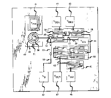
FIG. 3 shows a top view of the semiconductor chip containing the
circuit described in FIG. 2. This view is often called the mask pattern of the chip.
30 Shown on the chip pattern are a number of pads corresponding to DC bias and
output terminals in the circuit shown in FIG. 2. These are the VPIN pad 41, the
VA pad 42, the VDD I pad 43, the VSS 1 pad 44, the VDD2 pad 45, the V552 pad 46,and the Vovr pad n. The PlN part 48 of the circuit is located on the top left part
of the chip and consists of an opening 49 in the metal electrode and a donut-
35 shaped p-contact 50. Also shown (both under and to the side of the p-contact 50)
s71
- 6 -
is the p-conductivity region 51 which is part of the PIN junction. The p-contact is
electrically connected 52 to the gate of the MISFET shown 21 in FIG. 1 and
labeled 33 in FIG. 2. Also shown is electrical connection to the resistor 53 andthe electrical connestion 54 to the VB pad 42 corresponding to the PIN section
S shown in FIG. 2. Also shown are the active 55 and load 56 FETs of the amplifier
sections corresponding to the active 33 and load 34 FETs of FIG. 2. The gate andsource of the load FET 56is electrically connected 57 to the gate 58 of the active
FET of the buffer stage (35 in FIG. 2). The source of the active FET 55 of the
amplification stage is electrically connected to the Vss I pad 44 by means of a
10 conductor 59. The buffer stage is made up of an active FET 58 (35 in FIG. 2), a
senes of diodes 60 (37 in FIG. 2) and a load FET 61 (36 in FIC~. 2~. One side ofthe diode string 60 and the drain of the load ~ET 61 are connected together 62, as
well as to the VOVT pad.
Many other circuit arrangements are possible using the combination of
15 PIN photodiode and MISFET amplifier shown in nG. 1.
Typical reverse current-voltage (I-V) and capacitance-voltage (C-V)
characteristics of the PIN diodes are shown in FIGS. 4 and 5. The PIN diode is
of planar structure, and the leakage cu~rent is well below 10 nA at -10 V bias.
Leakage current as low as 100 pA at -10 V has been observed. The depletion
capacitance is less than 0.2 pF below -5 V bias. The quantum efficiency at 1.3~1m
wavelength is over 70% with index-matching epoxy. These results are sirnilar to
those of the PlN diodes fabricated from wafers with only trichloride VPE layers.In fact, the semi-insuladng InP as a cap layer may help to reduce the leakage
cu~ent.
The InP MISFET device is 100,~1m wide with a gate length of l~m.
It can be operated both in the enhancement and depletion mode. The I-V curves
show little hysteresis and complete pinch-off at -2 V. Near zero gate bias, the
transconductance is approximately 6 mS, i.e., 60 mS/mm. The gate capacitance at
zero bias is approximately 0.15 pF. The I-V characteristics of the load FET with30 gate and source connected together are also exceptionally good. The gate length
is 3~m, and the width is also 100~1m. The drain salturation current IDSs of the
load FET is around 9 mA which is slightly lower than that of the active FET of
10 mA. Both FETs have output impedances higher than 2 KQ.
37
- 7 -
The dc voltage transfer characte~istic for the comrnon source inverter
stage is of interest. The drain bias voltage is varied from 3.5V to 6.5V, and the
maximum gain is approximately 7.2 when biased at 6.5V. This agrees with the
calculated gain of A = gm x (RoU~/lR~!oad), where
S gm = 6mS and (Rou~l /Rload)=l 2kQ FIG. 6 shows the transfer characteristics ofthe buffer stage with four level-shif~ing diodes. The input is swept from 1.5V to
2.0V, which corresponds to the output voltage of the inverter stage with a supply
voltage between 4.5V and 5.5V. The gain of this buffer stage is about 0.8. The
four level-shifting diodes are made of Au/Cr-InP Schottky diodés. and a total
10 series resistance of -120Q, leaving much room for improvement. An alternativeapproach which is expected to have higher turn-on voltages, although with some
increase in processing complexity, is to use InP junction diodes. The output
impedance is estimated to be approximately 300S~, but it can be reduced to closeto 50Q when the amplifier is connected in a transimpedance configuration.
The voltage transfer characteristics of both inverter and buffer stages
together were also measured and shown in FIG. 7. The total gain is
approximately 5 (14 dB). It is apparent that the output dc voltage can be very
close to zero when the input voltage is zero, provided the amplifier is biased
properly. The linear gain range of about 0.3V corresponds to a maximum input
20 optical signal of -30~W.
The response of the detector-amplifier combination to optical signals
are also of interest. This type of measurement is made using a high speed CSBH
laser (1.55~m wavelength) and observing the output of the detector-amplifier
combination. The rise and fall times are estimated to be 20 np and 15 np,
25 respectively. The RC time constant is therefore approximately lOns, and the
bandwidth is approximately 18 MHz.
The PIN-AMP sensitivity was measured at 400 Mb/s and 1.55~am
wavelength. The integrated received signal was equalized and further amplified.
The bias condition for the PIN-AMP is adjusted to achieve the best sensitivity, not
30 necessarily for the highest gain of the amplifier. At a 10-9 bit-error rate, the
receiver sensitivity is approximately -27 dB~L